High critical-current density and scaling of phase-slip processes in YBaCuO nanowires
Abstract
YBaCuO nanowires were reproducibly fabricated down to widths of 50 nm. A Au/Ti cap layer on YBCO yielded high electrical performance up to temperatures above 80 K in single nanowires. Critical current density of tens of MA/cm2 at T = 4.2 K and of 10 MA/cm2 at 77 K were achieved that survive in high magnetic fields. Phase-slip processes were tuned by choosing the size of the nanochannels and the intensity of the applied external magnetic field. Data indicate that YBCO nanowires are rather attractive system for the fabrication of efficient sensors, supporting the notion of futuristic THz devices.
1 Introduction
Superconducting nanostructures operating at the liquid nitrogen temperature are very attractive for several applications in superconducting electronics. In particular high critical-temperature superconductor (HTS) nanowires not only have the advantage of high temperature operation, but in principle can be functionally scaled to smaller sizes [1, 2] thanks to their extremely short coherence lengths . Other intrinsic properties of these materials can play a relevant role too. For instance, their characteristic fast relaxation times [3] offer higher counting rates in photo-detection experiments when compared to traditional superconductors [4].
In this context reliable top-down fabrication techniques allowing a more direct integration of the HTS nanostructures into hybrid systems are of much interest. Here we analyze the electrical properties of a number of nanofabricated wires down to 50 nm in width. Our measurements show very good performance for single YBCO nanowires both in terms of critical temperature () and critical-current density () with excellent potential for sensor applications. Critical-current densities up to 70 MA/cm2 at T = 4.2 K and 10 MA/cm2 at 77 K were achieved on YBCO capped by a thin protective layer of Au/Ti. These are among the best results reported for single nanowires [5, 6, 7, 8] (see below). Contrary to other works [2], where even smaller sizes were achieved for of nanowires, in this case we isolated single nanowires, thus responding to a much wider range of requirements for circuit design.
2 Experimental details
We have employed YBCO thin films produced on various substrates through different deposition techniques (sputtering and reactive thermal co-evaporation [9]). For the aims of this work of demonstrating a reliable top-down technology to obtain single YBCO nanowires down to a width of 50 nm and the utility of using a Au cap layer, the properties of the thin films to privilege are rms roughness as low as possible, and absence of macroscopic impurities in the film. The initial values of and of unpatterned films are relevant but not crucial. In order to perform systematic experiments and reliably compare nanostructures realized on different samples, we have employed thin films produced on large areas by co-evaporation technique by Theva [11]. From the same wafer, it is possible to cut 20 samples of size of 5 mm x 5 mm with the same properties. In this work we focus on c-axis YBCO thin films (50 nm thick), grown on a seed layer (40 nm thick), and protected by a 20 nm thick Au layer [11]. The substrate is a large wafer of Yttria-stabilized zirconia (YSZ). The values of the original critical temperature and of the critical current density are high ( 86.5 K and = 2.2 at T= 77 K) but not optimized to the highest possible values. The key-steps of the nanotechnology approach are based on the use of a 30 nm thick Ti mask patterned through e-beam lithography (ZEISS MERLIN), and on a low energy milling procedure keeping the sample at a temperature of about -150. Most of the procedure is described in detail in [12]. All nanobridges described in this work are 1 m long. A comparative study of bare and capped YBCO nanowires on samples produced in the same deposition run and only differing by the last fabrication step (bare nanowires undergo an additional ion milling step in order to remove the Au layer) sheds light on the role of Au layer protecting the nanowires. The Au/Ti layer makes easier the integration of the YBCO component into hybrid structures because of its better compatibility with other materials as opposed to HTS. If only genuine superconducting properties are required, the YBCO capped nanowires can perfectly replace YBCO nanowires for most functions. Nano-fabrication techniques are not restricted, for the resolutions specified above, to any specific choice of the substrates usually employed for HTS thin films, or thin film deposition conditions, as long as surface roughness is below some thresholds, for instance lower than 5nm on a total thickness of 50 nm.
Measurements were performed in liquid helium using a four probe configuration. The set up employed is equipped with two stages of cold filters (copper powder and RC Pi filters with a cut-off frequency of the order of a few GHz and 160 MHz respectively).


3 Results and Discussions
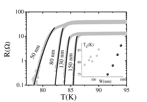
The critical temperature of various representative devices is reported as a function of wire width in the inset of Fig. 1. scales linearly for both types of bridges. For the capped YBCO, decreases from about 86 K for unpatterned films to about 85 (78) K for nanowires of width w= 140 (50) nm respectively. For the bare YBCO samples, of 1m wide bridges is basically the same of the unpatterned films and linearly decreases down to 75 K for nanowires of width w= 300 nm. Therefore the ’critical’ region is for widths below about 1 m. Superconductivity is quite robust also for widths less than 200 nm, but the properties of devices are less reproducible.
Not surprisingly, the bare YBCO thin films are more sensitive to ion milling and processing details. Figure 1 shows resistance vs temperature curves for the capped YBCO nanowires. Both bare and capped YBCO data can be well fitted in terms of the thermally-activated phase-slip model, i.e. the Langer- Ambegaokar- McCumber - Halperin (LAMH) model [13] commonly used to describe the broadening of R(T) in superconducting nanostructures [14]. The total resistance of the wire is commonly expressed as the parallel [14] between the resistance activated by phase-slip processes
| (1) |
and the normal resistance of quasiparticles [15]: . Here is the phase slipping rate, , is the quantum resistance constant, L is the sample length, is the Boltzmann constant, and is the free energy where the superconducting phase ”falls off”. at T=0 K can be expressed as (where A and are the cross section and the London penetration depth respectively) in analogy with other experiments on HTS nanowires [2]. The extracted values of the fitting parameters are and of which, are quite consistent with typical values of the cuprates [10]. F is for all curves about K.
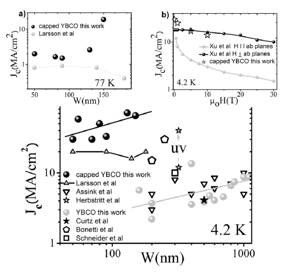
Measured critical-current density values are reported as a function of the width (w) for T = 4.2 K in Fig. 2 and compared with results available in literature [5, 6, 7, 8]. in capped YBCO nanowires is higher than 30 MA/cm2 (for w = 50 nm) and reaches a maximum of 70 MA/cm2 for W = 140 nm. These are among the highest values reported [5, 6, 8, 7] and only a few times lower than the theoretical depairing limit (300 MA/cm2) [16]. values at T = 77 K are reported in Fig. 2 inset a) for YBCO/Au/Ti nanowires and range from 2 MA/cm2 for w = 50 nm to 20 MA/cm2 for W = 140 nm. The better performances offered by capped nanowires when compared with those of bare YBCO nanowires of this and previous works [6], reveal that the protecting Au layer is key for enhancing the quality of HTS nanowires. We believe that there are margins to further improve performances especially at 77 K by employing films with higher values of the initial .
Nanowires keep good transport properties also when an external magnetic field is applied. For instance, in the extreme limit of 50 nm, a magnetic field of 10 T reduces by less than 10 %, while at 4.2 K is only halved. Superconductivity in 50 nm wide strips survives up to H = 1 T at 77 K. Figure 2 inset b) allows a comparison of the dependence of on magnetic field at T = 4.2 K [17] in the present samples with other results and confirms the robustness against an externally applied magnetic field. The use of HTS for power applications is a field of research of great relevance and a ’smart’ control of pinning centers is the key to increase . In macroscopic samples this role is usually played by the introduction of nanodefects [18, 19], while in nanowires by the detailed structure of the edge barrier [20].

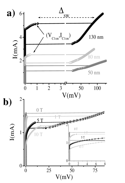
Figure 3a shows the experimental current-voltage (I-V) characteristics measured at T = 4.2 K for YBCO/Au/Ti nanowires 130, 80 and 50 nm wide. The distinctive feature is the presence of steps accompanied by a very large hysteresis that exceeds 30% of the total current. Similar features were reported by several author in experiments involving nanostructures [14] and HTS nanowires [2, 22, 23]. These observations were interpreted in terms of phenomena driving the superconducting channel to the normal state, i.e. the development of phase-slip centers (PSC) or normal hot spots (HP) [25]. Because of their low carrier density and thus low superfluid rigidity, HTS systems are inherently prone to phase fluctuations and therefore more susceptible to PSC in reduced dimensions [21, 14]. I-V curves reported in Fig. 3 show that the amplitude and the position of the steps depends on the size of the nanochannels and on the magnetic field. By increasing the width of the channel, the switch occurs at higher voltage. This is consistent with the idea that in wider samples the transition to the fast vortex motion that leads to the step structure occurs at a larger current [28]. As shown in Fig. 3b, an increase in H moves V1on to higher voltages to a maximum of about 15 mV for H = 10 T. The voltage jump is also reduced from = 80 mV at H = 0 T to about 10 mV at H = 10 T.
From the value of the critical voltage V1on=HL [26, 28] it is possible to estimate the vortex critical velocity = m/s (at H= 1 T), and hence the inelastic electron-electron scattering time on the basis of the expression [27], where D is the quasiparticle diffusion constant and . This value is in agreement with other experiments [27] and estimates [28].
The scaling of the I-V curves and of the steps with the width of the nano-channels and the influence of H on the I-Vs reflects the presence of phase slip lines (PSL) [29, 28]. PSL are a 2-dimensional analogue of PSC and reveal some kind of phase transition in the vortex lattice at the instability point with regions of fast and slow vortex motion [29, 28]. When the width of the bridges is reduced to w = 50 nm, the step position (V1on = 0) and the shape of the I-V indicate a transition from PSL to the more classical 1-dim PSC (at H = 0 T). In the narrowest nanowire, not more than one line of vortices at low fields can be hosted. When the magnetic field is increased, the size of inter-vortex distance () is decreased (for instance a = 20 nm at H = 5 T), and the entrance of additional rows of vortices is favored, with a consequent transition to PSL. This is documented by the steps at finite voltage in the presence of magnetic field (V 0). Vortex motion is characterized by oscillatory behavior of flux lines which cross the sample resulting in an emission of electromagnetic radiation that is on the order of Hz at H=1T.
Studies on the dynamics of kinematic vortex-antivortex lines confirm that their individual velocity can be manipulated by applying magnetic field and current [30], supporting the notion of futuristic THz devices.
4 Conclusions
In conclusion single YBCO nanowires were fabricated through a Au/Ti cap layer to reach very high values of the critical current density also at 77 K that is very robust against an externally applied magnetic field H. The detailed structures of the I-V curves of these single nanowires can be tuned by choosing the size of the bridge and by setting the magnetic field intensity. Threshold mechanisms associated to phase slips processes and visible as steps in I-Vs pave the way to HTS nanowires as sensors for photodetection experiments.
References
References
- [1] P. Mohanty, J. Y. T. Wei, V. Ananth, P. Morales, W. Skocpol, Physica C 408 410, 666 (2004).
- [2] Ke Xu and J.R.Heath, Nano Lett. 8, 3845 (2008).
- [3] M. Lindgren, M. Currie, C. A. Williams, T. Y. Hsiang, P. M. Fauchet, R. Sobolewski, S. H. Moffat, R. A. Hughes, J. S. Preston, and F. A. Hegmann, Appl. Phys. Lett. 74, 853 (1999).
- [4] G. Goltsman, O. Okunev, G. Chulkova, A. Lipatov, A. Semenov, K. Smirnov, B. Voronov, A. Dzardanov, C. Williams and R. Sobolewski, Appl. Phys. Lett. 79, 705 (2001); F. Marsili, D. Bitauld, A. Gaggero, R. Leoni, F. Mattioli, S. Hold, M. Benkahoul, F. Levy and A. Fiore, Opt. Express 16, 3191 (2008); M. Ejrnaes, R. Cristiano, O. Quaranta, S. Pagano, A. Gaggero, F. Mattioli, R. Leoni, B. Voronov and G. Gol’tsman Appl. Phys. Lett. 91, 262509 (2007).
- [5] J. A. Bonetti, D. S. Caplan, D. J. Van Harlingen, and M. B.Weissman, Phys. Rev. Lett. 93, 87002 (2008).
- [6] P. Larsson, B. Nilsson, and Z. G. Ivanov, J. Vac. Sci. Technol. B18, 25 (2000); J. Schneider, H. Kohlstedt, and R. Wordenweber, Appl. Phys. Lett. 63, 2426 (1993); H. Assink, A. J. M. v. d. Harg, C. M. Schep, N. Y. Chen, D. v. d. Marel, P. Hadley, E. W. J. M. v. d. Drift, and J. E. Mooij, IEEE Trans. Appl. Supercond. 3, 2983 (1993).
- [7] F. Herbstritt, T. Kemen, A. Marx, and R. Gross, J. Appl. Phys. 91, 5411 (2002).
- [8] J.N. Curtz, E. Koller, H. Zbinden, M. Decroux, L. Antognazza, O. Fischer and N. Gisin, Supercond. Sci. Technol. 23, 045015 (2010).
- [9] H. Kinder, P. Berberich, W. Prusseit, S. Rieder-Zecha, R. Semerad, B. Utz, Physica C 282-287, 107 (1997); R Semerad, J Knauf, K Irgmaier, W Prusseit , Physica C 378-381, 1414 (2002) (2010).
- [10] Superconductivity Physics and Applications, Kristian Fossheim and Asle Sudbø, (John Wisley & Sons, 2004).
- [11] Supplied by the company THEVA GmbH, Ismaning, Germany: www.theva.com.
- [12] G. Papari, F. Carillo, D. Born L. Bartoloni, E. Gambale, D. Stornaiuolo, P. Pingue, F. Beltram and F. Tafuri, IEEE Trans on Appl. Supercond. 19, 183 (2009).
- [13] J. S. Langer and V. Ambegaokar, Phys. Rev. 164, 498 (1967); D.E. McCumber and B.I. Halperin, Phys. Rev. B 1, 1054 (1970).
- [14] A. Bezryadin, J. Phys.: Condens. Matter 20, 043202 (2008); K. Yu. Arutyunov, D. S. Golubev and A. D. Zaikin, Phys. Rep. 464, 1 (2008).
- [15] W.A. Little Phys. Rev. 156, 396 (1967).
- [16] I. Puica, W. Lang, M. Peruzzi, K. v. Lemmermann, J. D. Pedarnig and D. Bauerle, Supercond. Sci. Techn. 17, S543 (2004); I. Maggio-Aprile, C. Renner, A. Erb, E. Walker and O. Fischer, Nature 390, 487 (1997).
- [17] A. Xu, J. J. Jaroszynski, F. Kametani, Z. Chen, D. C. Larbalestier, Y. L. Viouchkov, Y. Chen, Y. Xie and V Selvamanickam, Supercond. Sci. Technol. 23, 14003 (2010).
- [18] D. Christen Nature Materials 3, 421 (2004); S. R. Foltyn, L. Civale, J. L. MacManus-Driscoll, Q. X. Jia, B. Maiorov, H. Wang and M. Maley, Nature Materials 6, 631 (2007); J. Gutierrez, A. Llordes, J. Gazques, M. Gibert, N. Roma , S. Ricart, A. Pomar, F. Sandiumenge, N. Mestres, T. Puig AND X. Obradors, Nature Materials 6, 367 (2007).
- [19] X. Song, Z. Chen, S. Kim, D. M. Feldmann, D. Larbalestier, J. Reeves, Y. Xie and V. Selvamanickam, Appl. Phys. Lett. 88, 212508 (2006); A. Crisan, P. Badica, S. Fujiwara, J. C. Nie, A. Sundaresan, Y. Tanaka and H. Ihara Appl. Phys. Lett. 80, 3566 (2002).
- [20] S. Tahara, S. M. Anlange, J. Halbritter, C. B. Eom, D. K. Fork, T. H. Geballe, M. R. Beasley, Phys. Rev. B 41, 11203 (1990).
- [21] G. Blatter, M. V. Feigel’man, V. B. Gehkenbein, A. I. Larkin, V. M. Vinokur, Rev. Mod. Phys. 66, 1125 (1994).
- [22] P. Mikheenko, X. Deng, S. Gildert, M. S. Colclough, R. A. Smith, C. M. Muirhead, P. D. Prewett and J. Teng, Phys. Rev. B 72, 174506 (2005).
- [23] S. Reymond, L. Antognazza, M. Decroux, E. Koller, P. Reinert, and O. Fischer, Phys. Rev. B 66, 014522 (2002).
- [24] F. S. Jelila, J.-P. Maneval, F. R. Ladan, F. Chibane, A. Marie-de-Ficquelmont, L. M chin, J.-C. Villegier, M. Aprili, and J. Lesueur, Phys. Rev. Lett. 81, 1933 (1998).
- [25] W. J. Skocpol, M. R. Beasley, and M. Tinkham, J. Low Temp. Phys. 16, 145 (1974).
- [26] A. I. Larkin and Yu. N. Ovchinnikov, Zh. Eksp. Teor. Fiz. 68, 1915 (1975) [Sov. Phys. JETP 41, 960 (1976)]; A. I. Larkin and Yu. N. Ovchinnikov, in Nonequilibrium Superconductivity, edited by D. N. Langenberg and A. I. Larkin (Elsevier) (1986).
- [27] S. G. Doettinger, R. P. Huebener, R. Gerdemann, A. Kuhle, S. Anders, T. G. Trauble, and J. C. Villegier, Phys. Rev. Lett. 73, 1691 (1994); S. G. Doettinger, S. Kittelberger, R. P. Huebener, and C. C. Tsuei, Phys. Rev. B 56, 14157 (1997).
- [28] D. Y. Vodolazov and F. M. Peeters, Phys. Rev. B 76, 014521 (2007).
- [29] A. G. Sivakov, A. M. Glukhov, A. N. Omelyanchouk, Y. Koval, P. Muller, and A. V. Ustinov, Phys. Rev. Lett. 91, 267001 (2003).
- [30] G. R. Berdiyorov, M. V. Milo evi , and F. M. Peeters, Phys. Rev. B 79, 184506 (2009).