Electrically tunable band gap in silicene
Abstract
We report calculations of the electronic structure of silicene and the stability of its weakly buckled honeycomb lattice in an external electric field oriented perpendicular to the monolayer of Si atoms. The electric field produces a tunable band gap in the Dirac-type electronic spectrum, the gap being suppressed by a factor of about eight by the high polarizability of the system. At low electric fields, the interplay between this tunable band gap, which is specific to electrons on a honeycomb lattice, and the Kane-Mele spin-orbit coupling induces a transition from a topological to a band insulator, whereas at much higher electric fields silicene becomes a semimetal.
pacs:
73.22.Pr, 63.22.Rc, 61.48.GhI Introduction
Two-dimensional (2D) carbon crystals are hosts for Dirac-type electrons, whose unusual properties have been studied extensively in graphene monolayers produced by mechanical exfoliation from graphite.novoselov_2004 ; geim_2007 A close relative of graphene, a 2D honeycomb lattice of Si atoms called silicene,cahangirov does not occur in nature, but nanoribbons of silicene have been synthesized on metal surfaces.exp01 ; exp02 ; exp03 Due to the similarity of the lattice structures, the band structure of silicene resembles that of graphene, featuring Dirac-type electron dispersion in the vicinity of the corners of its hexagonal Brillouin zone (BZ).wallace Moreover, silicene has been shown theoretically to be metastable as a free-standing 2D crystal,cahangirov implying that it is possible to transfer silicene onto an insulating substrate and gate it electrically. In this work we predict the properties of this 2D crystal.
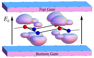
The similarity between graphene and silicene arises from the fact that C and Si belong to the same group in the periodic table of elements. However, Si has a larger ionic radius, which promotes sp3 hybridization, whereas sp2 hybridization is energetically more favorable in C. As a result, in a 2D layer of Si atoms, the bonding is formed by mixed sp2 and sp3 hybridization. Hence silicene is slightly buckled, with one of the two sublattices of the honeycomb lattice being displaced vertically with respect to the other, as shown in Fig. 1. Such buckling creates new possibilities for manipulating the dispersion of electrons in silicene and opening an electrically controlled sublattice-asymmetry band gap.ni2012 In this article we report density functional theory (DFT) calculations of the band gap for Dirac-type electrons in silicene opened by a perpendicular electric field using a combination of top and bottom gates. We show that can reach tens of meV before the 2D crystal transforms into a semimetal and then, at still higher fields, loses structural stability. We also determine the weak electric field at which electrons in silicene experience a transition from a topological insulator regimehasan_kane ; qi_2011 caused by the Kane-Mele spin-orbit (SO) couplingkane_mele for electrons on a honeycomb lattice into a conventional band insulator regime.
The rest of this article is arranged as follows. In Sec. II we report our results for the structural and electronic properties of free-standing silicene, and compare them with other theoretical and experimental results in the literature. In Sec. III we analyze the effects of a transverse electric field on the structural and electronic properties of silicene, and in Sec. IV we discuss the effects of SO coupling on the electronic structure, arguing that a crossover from topological insulating behavior to band insulating behavior must take place as the transverse field increases in strength. In Sec. V we give the technical details of our computational methodology and demonstrate the convergence of our results with respect to simulation parameters. Finally, we draw our conclusions in Sec. VI.
II Structural and electronic parameters of free-standing silicene
II.1 Comparison with theoretical and experimental results in the literature
The lattice constant and the (out-of-plane) coordinates of the Si atoms lying on the 2D honeycomb lattice were both fully relaxed using DFT (i) in the local density approximation (LDA), (ii) with the Perdew-Burke-Ernzerhof (PBE) exchange-correlation functional,pbe and (iii) with the screened Heyd-Scuseria-Ernzerhof 06 (HSE06) hybrid functional.hse ; hse2 Our DFT calculations were performed using the castepcastep ; castep_dfpt and vaspvasp plane-wave-basis codes, using ultrasoft pseudopotentials and the projector-augmented-wave (PAW) method, respectively. The -coordinates of the two Si atoms in the unit cell (the and sublattices) differ by a finite distance . Our results for a free silicene monolayer are shown in Table 1. The metastable lattice that we find is the same as the “low-buckled” structure found by Cahangirov et al.cahangirov
| Method | (Å) | (Å) | (eV) | ( ms-1) |
|---|---|---|---|---|
| PBE (castep) | ||||
| PBE (vasp) | ||||
| PBEni2012 | ||||
| LDA (castep) | ||||
| LDA (vasp) | ||||
| LDAcahangirov | ||||
| LDApan2011 | ||||
| HSE06 (vasp) | ||||
| Exp. [on Ag(110)]exp02 | ||||
| Exp. [on Ag(111)]exp03 |
II.2 Stability of free-standing silicene
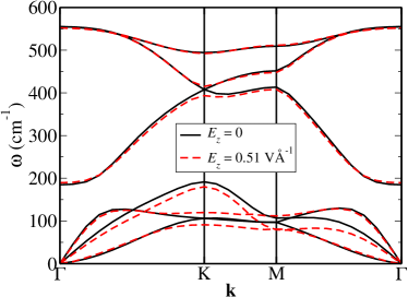
The cohesive energy of bulk Si (including a correction for the zero-point energy) has been calculated within DFT-LDA as 5.34 eV.alfe_2004 Comparing this with our DFT-LDA cohesive energy of silicene reported in Table 1 shows that bulk Si is substantially (0.22 eV per atom) more stable than silicene, implying that silicene would not grow naturally as a layered bulk crystal like graphite. However, by calculating the DFT phonon dispersion it has been verified both here and in Ref. cahangirov, that the structure is dynamically stable: no imaginary frequencies appear anywhere in the BZ. The results of such an analysis are summarized in Fig. 2. This convinces us that, as a metastable 2D crystal, silicene can be transferred onto an insulating substrate, where its electronic properties can be studied and manipulated as suggested below.
II.3 Electronic band structure
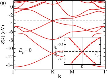
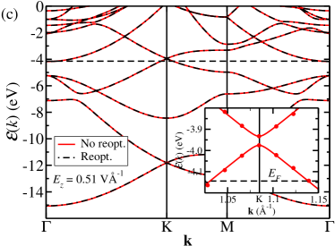
The calculated band structure of a “free” silicene layer is shown in Fig. 3. As expected, it resembles the band structure of graphene; in particular it shows the linear Dirac-type dispersion of electrons near the K points, where we find the Fermi level in undoped silicene. The Fermi velocity of electrons in silicene is lower than that in graphene (see Table 1). Although the lattice parameters and sublattice buckling found in the different DFT calculations are in good agreement, our results for the Fermi velocity are very much smaller than the Fermi velocity reported in Ref. cahangirov, .
III Application of a transverse electric field
III.1 Breaking the sublattice symmetry
To exploit the weak buckling of silicene, we consider its behavior in an external electric field applied in the -direction, as shown in Fig. 1. The main effect of such an electric field is to break the symmetry between the and sublattices of silicene’s honeycomb structure and hence to open a gap in the band structure at the hexagonal BZ points K and K′. In the framework of a simple nearest-neighbor tight-binding model, this manifests itself in the form of an energy correction to the on-site energies that is positive for sublattice and negative for . This difference in on-site energies leads to a spectrum with a gap for electrons in the vicinity of the corners of the BZ: , where is the electron “valley” momentum relative to the BZ corner. Opening a gap in graphene by these means would be impossible because the and sublattices lie in the same plane.
III.2 First-order perturbation theory
A naïve estimate of the electric-field-induced gap in silicene can be made using first-order perturbation theory by diagonalizing a Hamiltonian matrix at ,
| (1) |
Here, are the degenerate lowest unoccupied and highest occupied Kohn-Sham orbitals at the K point at , and corresponds to the mid-plane of the buckled lattice. This suggests a band gap which opens linearly with the electric field at a rate and 0.573 eÅ for the wave functions found using the LDA and PBE functionals, respectively.
III.3 Self-consistent DFT calculations in the presence of the field
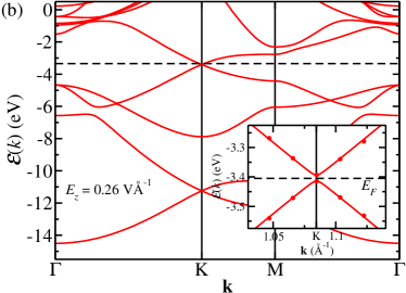
The estimate given in Sec. III.2 is in fact only an upper limit for the rate at which the band gap opens, since it neglects screening by the polarization of the and sublattices. In order to obtain an accurate value of the rate at which a band gap can be opened with an electric field, we have performed fully self-consistent calculations of the DFT band structure in the presence of an electric field. A typical result of such a calculation is shown in Fig. 3(b). At small electric fields, relaxing the structure in the presence of the field does not have a significant effect on the band gap, but the screening of the electric potential by the sublattice polarization of the electron states makes a substantial difference. The DFT-calculated gaps are gathered in Fig. 4. The variation of the band gap at K with electric field is almost perfectly linear for fields up to VÅ-1. The results for the rate at which a gap is opened are shown in the table inset in Fig. 4. The eightfold difference between the self-consistent and the unscreened values of indicates that the system exhibits a strong sublattice polarizability.
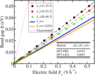
Our value for the rate at which the band gap opens within DFT-PBE is 0.0742 eÅ. This is substantially lower than the result obtained by Ni et al.,ni2012 which is 0.157 eÅ. Part of the reason for the discrepancy is that we extrapolated our results to infinite box length, whereas Ni et al. used a fixed amount of vacuum between the periodic images of the layers. Another possible reason for the difference is that we used a plane-wave basis set, whereas Ni et al. used a localized basis set. An incomplete localized basis set would tend to undermine the extent to which the electrons can adjust to screen the electric field.
III.4 Stability of the silicene lattice in an electric field
The narrow-gap silicene band structure shown in Fig. 3 persists over a broad range of electric fields . However, for electric fields of more than VÅ-1, the band gap starts to close due to an overlap of the conduction band at and the valence band at K, and silicene becomes a semimetal, as shown in Fig. 3(c). According to our calculations, the buckled honeycomb crystal is still metastable at this electric field, as can be seen in Fig. 2. The main effects of the electric field on the phonon dispersion curve are (i) to lift some degeneracies at K and M and (ii) to soften one of the acoustic branches, but without making the frequency imaginary. Under much higher electric fields, the honeycomb structure of silicene becomes unstable. We found that VÅ-1 causes the lattice parameter to increase without bound when the structure is relaxed.
IV SO coupling in silicene
IV.1 SO-induced gap
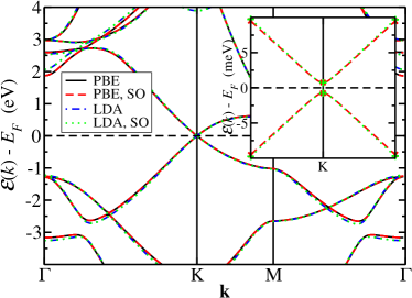
We have also performed a study of the effects of SO coupling (which is more pronounced in Si than in C) on the band structure. The SO coupling term is explicitly included in the Hamiltonian in the DFT calculations. The results obtained with the LDA and PBE functionals are shown in Fig. 5. Both functionals predict an SO gap of the order of a few meV at the K point, while the rest of the band structure barely differs from the nonrelativistic case. Our calculated LDA and PBE SO gaps are 1.4 meV and 1.5 meV, respectively, in agreement with the recent literature.liu_2011
IV.2 Crossover from topological to band insulating behavior
In the theory of Dirac electrons on the honeycomb lattice, the SO gap is accounted for by the Kane-Mele term describing, e.g., intrinsic SO coupling in graphene.kane_mele The Kane-Mele SO coupling and the electric-field induced - sublattice asymmetry for electrons in the vicinity of the BZ corners in silicene can be incorporated in the Hamiltonian
| (2) |
where distinguishes between the two valleys, and , in silicene’s spectrum. Here, the Pauli matrices , , and act in the space of the electrons’ amplitudes on orbitals attributed to the and sublattices, for the valley at and for the valley at . In Eq. (2), is the electron spin operator normal to the silicene plane, and and are the DFT-calculated SO-coupling and electric-field induced gaps.
The Hamiltonian of Eq. (2) generically describes the transition between the 2D topological and band-gap insulators. Its spectrum,
| (3) |
includes two gapped branches, one with a larger gap and another with a smaller gap . At a critical external electric field mVÅ-1, , and the smaller gap closes, marking a transition from a topological insulatorhasan_kane ; qi_2011 ; kane_mele at to a simple band insulator at . The difference between these two states of silicene is that the topological insulator state supports a gapless spectrum of edge states for the electrons, in contrast to a simple insulator, where the existence of gapless edge states is not protected by topology. However, one may expect something reminiscent of the topological properties of Dirac electrons to show up even in the band insulator state of silicene: an interface between two differently gated regions, with electric fields and (where ), should support a one-dimensional gapless band with an almost linear dispersion of electrons.semenoff
V Computational details
V.1 Cohesive energy
All our plane-wave DFT total energies were corrected for finite-basis errorfrancis and it was verified that the residual dependence of the total energy on the plane-wave cutoff energy is negligible. We used ultrasoft pseudopotentials throughout, except where otherwise stated. The silicene system was made artificially periodic in the -direction (normal to the silicene layer) in our calculations. The atomic structure was obtained by relaxing the lattice parameter and atom positions within DFT, subject to the symmetry constraints and at fixed box length in the direction. The cohesive energy was then evaluated using this optimized structure.
The energy of an isolated Si atom (needed when evaluating the cohesive energy) was obtained in a cubic box of side-length subject to periodic boundary conditions. We extrapolated the energy of the isolated atom to the limit of infinite box size by fitting
| (4) |
to the DFT energies obtained in a range of box sizes, where and were parameters determined by fitting. Equation (4) gave a very good fit to our data.
We have also calculated the DFT zero-point correction to the energy of silicene. This is expected to be largely independent of the exchange-correlation functional used. Indeed, our calculations show that the zero-point correction is 0.103 eV within the LDA and 0.101 eV with the PBE functional.pbe We used the PBE result in our final calculations of the cohesive energy reported in Table 1.
V.2 Evaluation of the Fermi velocity
To evaluate the Fermi velocity shown in Table 1 we evaluated the DFT band structure using a -point grid and a plane-wave cutoff energy of 816 eV in a cell of length Å. We then fitted Eq. (17) of Ref. winkler, to the highest occupied and lowest unoccupied bands within a circular region around the K point; the Fermi velocity is one of the fitting parameters. The radius of the circular region was 6% of the length of the reciprocal lattice vectors; we verified that the Fermi velocity was converged with respect to this radius.
V.3 Geometry optimization and phonon dispersion curves
The phonon dispersion curves shown in Sec. II.2 were calculated using the method of finite displacements, with atom displacements of 0.042 Å, in a supercell consisting of primitive cells with a -point grid in the primitive cell. In the results with the external electric field, the box length was Å and the plane-wave cutoff energy was 435 eV. In the results without the field, the box length was Å and the plane-wave cutoff was 816 eV. This choice was made because the error due to a finite box length is potentially much larger in the presence of a transverse electric field.
The geometry optimization and band-structure calculations at zero external field were performed with both the castepcastep ; castep_dfpt and vaspvasp codes, to verify that the results are in good agreement. This check was necessary because it was only possible to perform the electric-field calculations with castep, while for the SO calculations we had to use vasp. In principle the only difference between the calculations performed using the two codes arises from the Si pseudopotentials used. The PAW methodblochl was used in the vasp calculations, whereas ultrasoft pseudopotentials were used in the castep calculations. As can be seen in Table 1, the geometries predicted by the two codes agree well. We have also verified that the band structures are in good agreement. Finally, in Fig. 6 we show that the phonon dispersions obtained with the two codes are virtually identical when the same parameters are used.
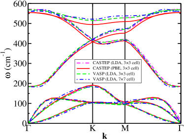
Figure 6 also demonstrates that our phonon dispersion curves are converged with respect to supercell size.
V.4 Band gap in the presence of an external electric field
V.4.1 Plane-wave cutoff energy
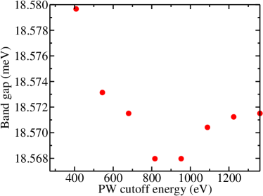
The convergence of the calculated band gap with respect to the plane-wave cutoff energy for a particular applied field is shown in Fig. 7. The gap converges extremely rapidly.
V.4.2 k-point sampling
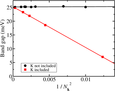
The convergence of the calculated band gap at BZ point K with respect to the -point grid used in the self-consistent field calculations is shown in Fig. 8. The finite-sampling error falls off as the reciprocal of the total number of points. The prefactor of the finite-sampling error is vastly greater when K or K′ is included in the grid of -points for the self-consistent field calculations.
V.4.3 Choice of pseudopotential
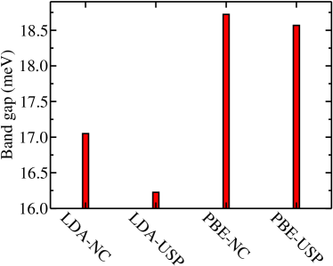
The dependence of the calculated gap on the exchange-correlation functional and pseudopotential is shown in Fig. 9. The difference between the results obtained with different pseudopotentials is much smaller than the gap, but is not wholly negligible. The on-the-fly ultrasoft pseudopotential is believed to be more accurate than the norm-conserving pseudopotential,castep and hence we have used the former in our final calculations.
V.4.4 Box length
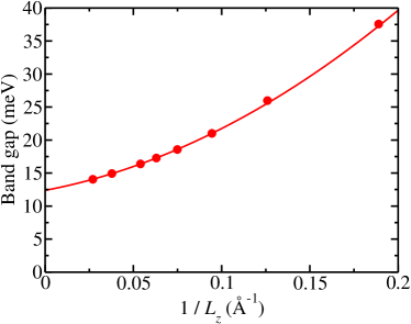
The dependence of the calculated gap on the length of the simulation box is shown in Fig. 10. It is clear that this is potentially a large source of error. However, the -dependence is reasonably well approximated by a quadratic in , allowing the DFT gaps to be extrapolated to infinite cell size if results at three or more different cell sizes are available.
V.4.5 Estimates of uncertainty in our final results
Our final results for the field-induced gap were obtained using points, not including K or K′, a plane-wave cutoff energy of eV, and box lengths , 18.521, and 26.459 Å; the results were then extrapolated to infinite box length by fitting a quadratic in . From the magnitudes of the variations shown in Figs. 7–10, we estimate the uncertainty in our final results for the rate at which the band gap opens when an electric field is applied to be less than about 0.01 eÅ.
V.5 Unscreened estimate of the band gap in the presence of an external electric field
To evaluate the field-induced band gap using perturbation theory we used norm-conserving pseudopotentials.castep We used a -point mesh including the K point, and a cell length of Å. It was verified that the perturbation-theory-induced rate of gap opening was converged to within 0.00002 eÅ with respect to -point mesh and . The finite-basis error in was found to fall off approximately exponentially with respect to the plane-wave cutoff energy, and hence we extrapolated our results to basis-set completeness.
V.6 Band structure with SO coupling
The SO calculations were performed with a plane-wave cutoff of 500 eV and a -point grid. We checked that the length of the simulation box has negligible influence on the SO gap: the gap is the same with simulation box lengths of 15 Å and 30 Å up to numerical accuracy.
VI Conclusions
In summary, we have shown that a 2D layer of Si atoms—silicene—is a versatile material in which a band gap can be tuned (in a broad range of tens of meV) using a transverse electric field , while silicene remains metastable. At the low field mVÅ-1, we expect silicene to undergo a transition between a topological and a simple band insulator, whereas at much higher field VÅ-1 it will undergo a transition from a band insulator into a semimetal.
Acknowledgements.
We acknowledge financial support from the EPSRC through a Science and Innovation Award, the EU through the grants Concept Graphene and CARBOTRON, the Royal Society, and Lancaster University through the Early Career Small Grant Scheme. Computational resources were provided by Lancaster University’s High-End Computing facility. We thank H.-J. Gao and G. Le Lay for useful discussions, and J. R. Wallbank for providing us with Fig. 1.References
- (1) K. S. Novoselov, A. K. Geim, S. V. Morozov, D. Jiang, Y. Zhang, S. V. Dubonos, I. V. Grigorieva, and A. A. Firsov, Science 306, 666 (2004).
- (2) A. K. Geim and K. S. Novoselov, Nature Materials 6, 183 (2007).
- (3) S. Cahangirov, M. Topsakal, E. Aktürk, H. Şahin and S. Ciraci, Phys. Rev. Lett. 102, 236804 (2009).
- (4) B. Aufray, A. Kara, S. Vizzini, H. Oughaddou, C. Léandri, B. Ealet, and G. L. Lay, Appl. Phys. Lett. 96, 183102 (2010).
- (5) P. E. Padova, C. Quaresima, C. Ottaviani, P. M. Sheverdyaeva, P. Moras, C. Carbone, D. Topwal, B. Olivieri, A. Kara, H. Oughaddou, B. Aufray, and G. L. Lay, Appl. Phys. Lett. 96, 261905 (2010).
- (6) B. Lalmi, H. Oughaddou, H. Enriquez, A. Kara, S. Vizzini, B. Ealet, and B. Aufray, Appl. Phys. Lett. 97, 223109 (2010).
- (7) P. R. Wallace, Phys. Rev. 71, 622 (1947).
- (8) Z. Ni, Q. Liu, K. Tang, J. Zheng, J. Zhou, R. Qin, Z. Gao, D. Yu, and J. Lu, Nano Lett. 12, 113 (2012).
- (9) M. Z. Hasan and C. L. Kane, Rev. Mod. Phys. 82, 3045 (2010).
- (10) X.-L. Qi and S.-C. Zhang, Rev. Mod. Phys. 83, 1057 (2011).
- (11) C. L. Kane and E. J. Mele, Phys. Rev. Lett. 95, 226801 (2005).
- (12) J. P. Perdew, K. Burke, and M. Ernzerhof, Phys. Rev. Lett. 77, 3865 (1996).
- (13) J. Heyd, G. E. Scuseria, and M. Ernzerhof, J. Chem. Phys. 118, 8207 (2003).
- (14) A. V. Krukau, O. A. Vydrov, A. F. Izmaylov, and G. E. Scuseria, J. Chem. Phys. 125, 224106 (2006).
- (15) S. J. Clark, M. D. Segall, C. J. Pickard, P. J. Hasnip, M. I. J. Probert, K. Refson, and M. C. Payne, Z. Kristallogr. 220, 567 (2005).
- (16) K. Refson, P. R. Tulip, and S. J. Clark, Phys. Rev. B 73, 155114 (2006).
- (17) G. Kresse and J. Furthmüller, Phys. Rev. B 54, 11169 (1996).
- (18) L. Pan, H. J. Liu, Y. W. Wen, X. J. Tan, H. Y. Lv, J. Shi, and X. F. Tang, Phys. Lett. A 375, 614 (2011).
- (19) D. Alfè, M. J. Gillan, M. D. Towler, and R. J. Needs, Phys. Rev. B 70, 214102 (2004).
- (20) C.-C. Liu, W. Feng, and Y. Yao, Phys. Rev. Lett. 107, 076802 (2011).
- (21) G. W. Semenoff, V. Semenoff, and F. Zhou, Phys. Rev. Lett. 101, 087204 (2008).
- (22) G. P. Francis and M. C. Payne, J. Phys.: Condens. Matter 2, 4395 (1990).
- (23) R. Winkler and U. Zülicke, Phys. Rev. B 82, 245313 (2010).
- (24) P. E. Blöchl, Phys. Rev. B 50, 17953 (1994).