Experimental verification of PbBi2Te4 as a 3D topological insulator
Abstract
The first experimental evidence is presented of the topological insulator state in PbBi2Te4. A single surface Dirac cone is observed by angle-resolved photoemission spectroscopy (ARPES) with synchrotron radiation. Topological invariants are calculated from the ab initio band structure to be 1; (111). The observed two-dimensional iso-energy contours in the bulk energy gap are found to be the largest among the known three-dimensional topological insulators. This opens a pathway to achieving a sufficiently large spin current density in future spintronic devices.
pacs:
73.20.-r, 79.60.-i
Topological insulators (TIs) have recently emerged as a new state of quantum matter, which are distinguished from conventional insulators by having a surface state with a massless Dirac dispersion in the bulk energy gap. The spin orientation of the topological surface state is locked with its crystal momentum, resulting in a helical spin texture. This new state can be classified by so-called topological invariants FKM_07 ; FK_07 . Generally, the massless Dirac cone can be created at an interface of two materials: a topological and an ordinary insulator. The unique properties of topological surface electrons provide a fertile ground to realize new electronic phenomena, such as a magnetic monopole arising from the topological magneto-electric effect and Majorana fermions at the interface with a superconductor Hasan&Kane_RMP ; Qi&Zhang_RMP . Owing to time-reversal symmetry, topological surface states are protected from backscattering in the presence of a weak perturbation, which is required for the realization of dissipationless spin transport without external magnetic fields in novel quantum devices Xue_11 ; Xiu_11 .
A number of materials that hold spin-polarized surface Dirac cones have been intensively studied, such as Bi1-xSbx Hsieh_Science_09 ; Nishide_PRB_10 , Bi2Te3 Chen_Science_09 ; Hsieh_PRL2009 , Bi2Se3 Xia_NatPhys_09 ; Kuroda_PRL_10_Bi2Se3 ; Bi2Se3_eph ; Kim_PRL_11 , and thallium-based compounds eremeev1 ; Eremeev_Tl_PRB2011 ; Kuroda_PRL_10_TlBiSe2 ; Yan_EPL_10 ; Lin_PRL_10 ; Sato_PRL_10 ; Chen_PRL_10 . Among them, Bi2Se3 has been regarded as one of the most promising candidates for potential applications in ultra-low power consumption quantum devices that can work stably at room temperature due to a sufficiently large bulk energy gap. Although significant efforts have been made towards spintronic applications, the surface contribution to conduction was hardly observed even at low bulk carrier density Analytis_PRB_10 ; Eto_PRB_10 ; Butch_PRB_10 . This motivates the search of new topological insulators with higher density of spin-polarized Dirac fermions.
Recently, some of the Pb-based ternary chalcogenides have been proposed as 3D topological insulators Eremeev_JETP_10 ; Jin_PRB_11 ; Menshchikova_JETP_11 . The present study is focused on PbBi2Te4, which has the simplest crystal structure among them. The crystal is composed of seven-layer blocks with the atomic layer sequence Te-Bi-Te-Pb-Te-Bi-Te [see Fig. S1(a) of supplementary material (SM)] Shelimova_PRB_11 . The theoretical analysis of Ref. Menshchikova_JETP_11 indicates that this compound is a three-dimensional (3D) topological insulator. In this Letter, we report the first experimental evidence of the topological surface state in PbBi2Te4 by angle-resolved photoemission spectroscopy (ARPES). We establish that the size of the two-dimensional iso-energy contour, which is proportional to the surface carrier density, is the largest among the known 3D topological insulators. Thus, PbBi2Te4 can be counted as one of the most promising candidates for realizing a large spin current density in future spintronic devices.
A single crystalline sample of PbBi2Te4 was grown by the standard procedure using Bridgman method [see SM for more details]. For ARPES measurement the samples were in situ cleaved along the basal plane. Photoemission experiment was performed with synchrotron radiation at the linear undulator beamline (BL1) and the helical undulator beamline (BL9A) of Hiroshima Synchrotron Radiation Center (HiSOR). The ARPES spectra were acquired with a hemispherical photoelectron analyzer (VG-SCIENTA R4000) at 17 K. The overall energy and angular resolutions were set to 10–20 meV and 0.3∘, respectively.
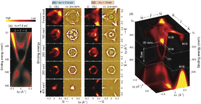
Figure 1(a) shows the ARPES energy dispersion curve along the line of the surface Brillouin zone [see SM, Fig. S1(b)] measured at eV. The parabolic band with the energy minimum at the binding energy of meV is seen to exhibit a rather strong photoemission intensity near the point. The position of the energy minimum does not change with the photon energy [see SM, Figs. S2(a) and S2(b)], which confirms the two-dimensional nature of this electronic state. More importantly, a linearly dispersing feature, i.e. the Dirac cone with the crossing point at meV is observed.
Figures 1(b) and 1(c) summarize the constant energy contours (i) and their second derivatives (ii) in the range Å Å-1 from meV (Dirac point) to 0 (Fermi level) at and 10 eV, respectively. With eV we find at the Dirac point energy six ellipses oriented along in addition to the point-like feature at the point for the Dirac state. On the other hand, the elliptical contours are much weaker at eV, signifying a strong matrix elements effect. In going away from the Dirac point, the sole hexagonally shaped contour is observed down to meV and at smaller binding energies another state becomes enclosed inside the Dirac cone (starting with meV). It is interpreted as the onset of the bulk conduction band (BCB) because the shape of the inner contours considerably depends on the photon energy, see Figs. 1(b) and 1(c). Below meV the Dirac cone further deforms and practically merges into the bulk conduction band. In the map measured with eV the hexagonal Fermi surface of the Dirac cone encloses two large and one small triangular shaped surfaces centered at . At eV the shape of the inner Fermi surfaces strongly changes and becomes very complicated, which is consistent with a bulk state [see Fig. S4 of SM]. The size of the energy gap is estimated as 230 meV as shown in the 3D map for eV [Fig. 1(d)]. Such a large energy gap is beneficial for a high stability of the spin current conductance at room temperature. Figure 1(d) illustrates a high anisotropy of the bulk valence band: the valence band maximum in the line is at meV ( Å-1), while in the line it is deeper in energy.
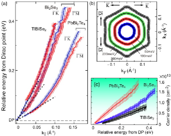
Next we discuss the surface Dirac cone of PbBi2Te4 in more detail by comparing it with other 3D TIs. The Dirac cone dispersion along and is shown in Fig. 2(a) for PbBi2Te4 and for the well studied TIs Bi2Se3 and TlBiSe2. Close to the Dirac cone energy dispersion in PbBi2Te4 is as steep as in the other materials, but it is apparently less steep near the Dirac point. In PbBi2Te4, the group velocity at is estimated as m/s, while near the Dirac point, it is much lower ( m/s) than in Bi2Se3 ( m/s) Kuroda_PRL_10_Bi2Se3 and in TlBiSe2 ( m/s) Kuroda_PRL_10_TlBiSe2 . The sizes of the iso-energy contours in the bulk energy gap from the Dirac point to 200 meV are much larger for PbBi2Te4 than for the other two materials, as shown in Fig .2(b). The estimated topological surface carrier density in PbBi2Te4 obtained from the area of constant energy contour is much larger than in the other two materials [Fig. 2(c)].


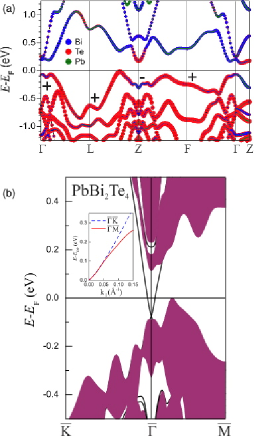
The theoretical bulk and surface band structures of PbBi2Te4 are shown in Figs. 3(a) and 3(b), respectively. The calculations were performed with the VASP code VASP ; PAW with optimized internal lattice parameters. In principle, three-dimensional materials with inversion symmetry are classified with four topological invariants , which can be determined by the parity of occupied bands at eight time-reversal invariant momenta (TRIM) , where , , are primitive reciprocal lattice vectors, and or 1 FKM_07 ; FK_07 . The invariants are determined by the equations and , where FK_07 . For rhombohedral lattice of PbBi2Te4 the TRIMs are , Z, and three equivalent L as well as F points [see SM, Fig. S1(b)]. The previous study confirmed that this compound is a strong topological insulator with the principal topological invariant Menshchikova_JETP_11 . Here we analyze the invariants. Interestingly, the parity inversion of bulk bands occurs at the Z point for PbBi2Te4 [Fig. 3(a)], which leads to invariants 1; (111). This is in contrast to the case of binary chalcogenides Bi2X3 (X=Se, Te), where the parity inversion takes place at the point with invariant 1; (000) Hasan&Kane_RMP . Note that PbBi2Te4 is the first case among the experimentally established topological insulators with invariant 1; (111) possessing a single Dirac cone surface state. It is, thus, distinguished from the Bi1-xSbx alloy with the same invariant Teo_08 but with 5 or 3 pairs of surface states crossing the Fermi energy Hsieh_Science_09 ; Nishide_PRB_10 . In Bi1-xSbx, owing to nonzero invariants , a one-dimensional (1D) topologically protected state can exist at the dislocation core Ran_09 . In the case of the layered crystal the bulk dislocations can hardly exist, but other types of 1D TI states, such as edge states in thin films or 1D states at step edges are possible.
Finally, we compare the experimental ARPES results with the theoretical band structures, see Fig. 3(b). The calculated band structure well reproduces the bulk conduction band minimum located at point at 200 meV above the Dirac point. Although the bulk valence band maximum is higher in theory than in experiment, the theory well reproduces its location in -space, that is, it appears around 1/3 ( Å-1). Anisotropic features along different symmetry lines can be recognized above 100 meV relative to the Dirac point, as depicted in the inset. In addition, the parabolic surface state appears at meV above the Dirac point in the conduction band gap, which is consistent with the present observation [see SM, Fig.S3].
Our conclusion led by the present experiment is twofold: (i) PbBi2Te4 is proved to be a three-dimensional topological insulator with the energy gap of 230 meV and a single Dirac cone at the point. (ii) The size of the Fermi surface contour in the bulk energy gap is significantly larger than in the other presently known 3D topological insulators, whereby the highest carrier density of the known topological surface states is achieved. These novel findings pave a way for the efficient control of the group velocity with sufficiently large spin current density by tuning the chemical potential in the bulk energy gap.
We thank Shuichi Murakami for valuable comments. We also thank J. Jiang, H. Hayashi, T. Habuchi and H. Iwasawa for their technical support in the ARPES measurement at Hiroshima Synchrotron Radiation Center (HSRC). This work was financially supported by KAKENHI (Grant No. 20340092, 23340105), Grant-in-Aid for Scientific Research (B) of JSPS. We also acknowledge partial support by the Department of Education of the Basque Country Government, the University of the Basque Country (project GV-UPV/EHU, grant IT-366-07), Ministerio de Ciencia e Inovación (grant FIS2010-19609-C02-00). Calculations were performed on SKIF-Cyberia (Tomsk State University) and Arina (UPV/EHU) supercomputers. The ARPES measurement was performed with the approval of the Proposal Assessing Committee of HSRC (Proposal No.11-A-3, 11-A-4). The SPring-8 experiments were carried out with the approval of the Japan Synchrotron Radiation Research Institute (JASRI) (Proposal No. 2010B0084, 2011A0084).
References
- (1) L. Fu, C.L. Kane, and E.J. Mele, Phys. Rev. Lett. 98, 106803 (2007).
- (2) L. Fu, and C.L. Kane, Phys. Rev. B 76, 045302 (2007).
- (3) M.Z. Hasan, and C.L. Kane, Rev. Mod. Phys. 82, 3045 (2010).
- (4) X.L. Qi, and S.C. Zhang, Rev. Mod. Phys. 83, 1057 (2011).
- (5) Q.K. Xue, Nat. Nanotechnol. 6, 197 (2011).
- (6) F. Xiu, L. He, Y. Wang, L. Cheng, L.T. Chang, M. Lang, G. Huang, X. Kou, Y. Zhou, X. Jiang, Z. Chen, J. Zou, A. Shailos, and K.L. Wang, Nat. Nanotechnol. 6, 216 (2011).
- (7) D. Hsieh, Y. Xia, L. Wray, D. Qian, A. Pal, J.H. Dil, J. Osterwalder, F. Meier, G. Bihlmayer, C.L. Kane, Y.S. Hor, R.J. Cava, and M.Z. Hasan, Science 323, 919 (2008).
- (8) A. Nishide, A.A. Taskin, Y. Takeichi, T. Okuda, A. Kakizaki, T. Hirahara, K. Nakatsuji, F. Komori, Y. Ando, and I. Matsuda, Phys. Rev. B 81, 041309 (2010).
- (9) Y.L. Chen, J.G. Analytis, J.-H. Chu, Z.K. Liu, S.-K. Mo, X.L. Qi, H.J. Zhang, D.H. Lu, X. Dai, Z. Fang, S.C. Zhang, I.R. Fisher, Z. Hussain, Z.-X. Shen, Science 325, 178 (2009).
- (10) D. Hsieh, Y. Xia, D. Qian, L. Wray, F. Meier, J.H. Dil, J. Osterwalder, L. Patthey, A.V. Fedorov, H. Lin, A. Bansil, D. Grauer, Y.S. Hor, R.J. Cava, and M.Z. Hasan, Phys. Rev. Lett. 103, 146401 (2009).
- (11) Y. Xia, D. Qian, D. Hsieh, L. Wray, A. Pal, H. Lin, A. Bansil, D. Grauer, Y.S. Hor, R.J. Cava and M.Z. Hasan, Nature Phys. 5, 398 (2009).
- (12) K. Kuroda, M. Arita, K. Miyamoto, M. Ye, J. Jiang, A. Kimura, E.E. Krasovskii, E.V. Chulkov, H. Iwasawa, T. Okuda, K. Shimada, Y. Ueda, H. Namatame, and M. Taniguchi, Phys. Rev. Lett. 105, 076802 (2010).
- (13) R.C. Hatch, M. Bianchi, D. Guan, S. Bao, J. Mi, B.B. Iversen, L. Nilsson, L. Hornekær, and P. Hofmann, Phys. Rev. B 83, 241303(R) (2011).
- (14) S. Kim, M. Ye, K. Kuroda, Y. Yamada, E.E. Krasovskii, E.V. Chulkov, K. Miyamoto, M. Nakatake, T. Okuda, Y. Ueda, K. Shimada, H. Namatame, M. Taniguchi, and A. Kimura, Phys. Rev. Lett. 107, 056803 (2011).
- (15) S.V. Eremeev, Yu.M. Koroteev, and E.V. Chulkov, Pis′ma Zh. Eksp. Teor. Fiz. 91, 664 (2010) [JETP Lett. 91, 594 (2010)].
- (16) S.V. Eremeev, G. Bihlmayer, M. Vergniory, Yu.M. Koroteev, T.V. Menshchikova, J. Henk, A. Ernst, and E.V. Chulkov, Phys. Rev. B 83, 205129 (2011).
- (17) K. Kuroda, M. Ye, A. Kimura, S.V. Eremeev, E.E. Krasovskii, E.V. Chulkov, Y. Ueda, K. Miyamoto, T. Okuda, K. Shimada, H. Namatame, and M. Taniguchi, Phys. Rev. Lett. 105, 146801 (2010).
- (18) B. Yan, C.X. Liu, H.J. Zhang, C.Y. Yam, X.L. Qi, T. Frauenheim, and S.C. Zhang, Euro Phys. Lett. 90, 37002 (2010).
- (19) H. Lin, R.S. Markiewicz, L.A. Wray, L. Fu, M.Z. Hasan, and A. Bansil, Phys. Rev. Lett. 105, 036404 (2010).
- (20) T. Sato, K. Segawa, H. Guo, K. Sugawara, S. Souma, T. Takahashi, and Y. Ando, Phys. Rev. Lett. 105, 136802 (2010).
- (21) Y.L. Chen, Z.K. Liu, J.G. Analytis, J.H. Chu, H.J. Zhang, B.H. Yan, S.K. Mo, R.G. Moore, D.H. Lu, I.R. Fisher, S.C. Zhang, Z. Hussain, and Z.X. Shen, Phys. Rev. Lett. 105, 266401 (2010).
- (22) J.G. Analytis, J.H. Chu, Y. Chen, F. Corredor, R.D. McDonald, Z.X. Shen, and I.R. Fisher, Phys. Rev. B 81, 205407 (2010).
- (23) K. Eto, Z. Ren, A.A. Taskin, K. Segawa, and Y. Ando, Phys. Rev. B 81, 195309 (2010).
- (24) N.P. Butch, K. Kirshenbaum, P. Syers, A.B. Sushkov, G.S. Jenkins, H.D. Drew, and J. Paglione, Phys. Rev. B 81, 241301(R) (2010).
- (25) S.V. Eremeev, Yu.M. Koroteev, and E.V. Chulkov, Pis′ma Zh. Eksp. Teor. Fiz. 92, 183 (2010) [JETP Lett. 92, 161 (2010)].
- (26) H. Jin, J.H Song, A.J. Freeman, and M.G. Kanatzidis,Phys. Rev. B 83, 041202(R) (2011).
- (27) T.V. Menshchikova, S.V. Eremeev, Yu.M. Koroteev, V. M. Kuznetsov, and E.V. Chulkov, Pis′ma Zh. Eksp. Teor. Fiz. 93, 18 (2010) [JETP Letters 93, 15 (2011)].
- (28) L.E. Shelimova, O.G. Karpinskii, T.E. Svechnikova, E.S. Avilov, M.A. Kretova, and V.S. Zemskov, Neorg. Mater. 40, 1440 (2004) [Inorg. Mater. 40, 1264 (2004).]
- (29) G. Kresse, J. Furthmüller, Comput. Mater. Sci. 6, 15 (1996).
- (30) G. Kresse, D. Joubert, Phys. Rev. B 59, 1758 (1999).
- (31) J.C.Y. Teo, L. Fu, and C.L. Kane, Phys. Rev. B 78, 045426 (2008).
- (32) Y. Ran, Y. Zhang, and A. Vishwanath, Nat. Phys. 5, 298 (2009).