Correlated magnetic states in domain and grain boundaries in graphene
Abstract
Ab initio calculations indicate that while the electronic states introduced by grain boundaries in graphene are only partially confined to the defect core, a domain boundary introduces states near the Fermi level that are very strongly confined to the core of the defect, and that display a ferromagnetic ground state. The domain boundary is fully immersed within the graphene matrix, hence this magnetic state is protected from reconstruction effects that have hampered experimental detection in the case of ribbon edge states. Furthermore, our calculations suggest that charge transfer between one-dimensional extended defects and the bulk in graphene is short ranged for both grain and domain boundaries.
pacs:
73.22.-f, 73.20.Hb, 71.55.-i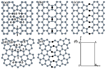
Controlling electronic transport and tailoring magnetic states at the nanoscale in graphene rank among the main issues related to the prospective application of this material in nanoelectronics and spintronics. In particular, electronic and magnetic states of extended line defects in graphene have been considered as possible conducting one-dimensional (1D) electronic channels and platforms for tailored spin states for spintronic applications. ahcn1 ; lahiri Two recent developments highlight the focus on extended line defects: (i) the recognition that mass-scale production of graphene should inevitably lead to a polycrystalline material, containing one-dimensional grain boundaries (GB) yu ; and (ii) the recent theoretical prediction umesh and experimental realization of domain boundaries (DB) in graphene by controlled deposition of the material on metallic substrates lahiri . In the case of GB’s, a large volume of works has accumulated in the last few years jsa ; simonis ; cervenka ; louie1 , while for the DB produced in Lahiri et al. experiment, valley-filter properties gunlycke and its effects on the magnetic edge states of a graphene ribbon lin have been theoretically investigated. Further, when chemical reduction of a readily available material, such as graphene oxide, is used as a viable route for mass-scale graphene synthesis cristina ; bagri , the presence of residual functional groups should affect the material electronic and magnetic properties.
In this context, the nature of the electronic states introduced by such extended 1D defects in graphene is a topic that deserves close inspection. More specifically, whether GB’s and DB’s act as quasi-1D conducting channels immersed in the bulk of graphene is the question we seek to address in this work. We also consider the issue of self-doping in graphene induced by the presence of such extended 1D defects prb06 , that occurs when the line defect attracts charge carriers, resulting in charged defective lines surrounded by a doped graphene matrix.
Our calculations indicate that while the electronic states introduced by a model GB structure in graphene hybridize with the bulk states and are only partially confined to the defect core, the DB defect introduces a sharp resonance in the density of states (DOS) of graphene, that lies just above the Fermi level in the neutral system, and is associated to electronic states that are very strongly confined to the core of the defect. Our results suggest that, when a graphene sample containing a DB is doped and these quasi-1D states are populated, a ferromagnetic state is realized, which is confined to zigzag chains along the defect core that are fully immersed within a bulk graphene matrix. The quantum confinement induced by the presence of a domain boundary leads to an enhancement of the Coulomb interactions and stronger electron-electron correlations. Because of their 1D nature, these correlated states do not show long range order. Instead, they present power law or algebraic correlation functions. Furthermore, given that these 1D states are immersed in a metallic environment, they are unique examples of open Luttinger liquids oll .
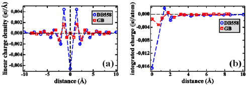
Moreover, we find that charge transfer between bulk graphene and the line defects is essentially local, with charge redistribution taking place within a region of 3-5 Å from the geometric center of the 1D defects. Both this charge-transfer region and the surrounding bulk regions remain essentially neutral. The absence of a charge monopole moment means that these 1D defects should act as weak charge carrier scatterers, in agreement with recent transport experiments in graphene grown by chemical vapor deposition (CVD) cvd .
In this study, we examine the nature of the electronic states introduced by the two aforementioned types of extended 1D defects in graphene: (i) large-angle tilt grain boundaries simonis ; cervenka , expected to occur commonly in mass-scale production of graphene; (ii) domain boundaries produced by deposition of a graphene layer on a Nickel substrate umesh ; lahiri . For both 1D defects, we also consider oxidized forms, with oxygen atoms bound to the atoms at the core of the defect. Figure 1(a) shows the atomistic model for the domain boundary defect, which consists of periodic units composed of one octagon and two side-sharing pentagons along the defect line, which we label DB558 in the following discussion. The oxidized forms with one (DB558+O) and two oxygen atoms (DB558+2O) per defect unit are shown respectively in Figs. 1(b) and (c). Figure 1(d) shows the GB model proposed in Ref. simonis, , while Fig. 1(e) shows the fully unzipped oxidized form of this defect (GB+O).
Our calculations are performed in the framework of Kohn-Sham density functional theory (DFT), within the generalized-gradient approximation (GGA) ks-gga and norm-conserving pseudopotentials in the Kleinman-Bylander factorized form tm-kb . We use the LCAO method implemented in the SIESTA code siesta , with a double-zeta basis set plus polarization orbitals. A Mulliken charge partition is employed for the analysis of the charge-transfer between bulk and defects. Supercells of 66 (84) atoms are employed for the DB558 (GB) calculations. We performed convergence tests to ensure that, at these cell sizes, our results are not affected by interaction between the defects and their periodic images.
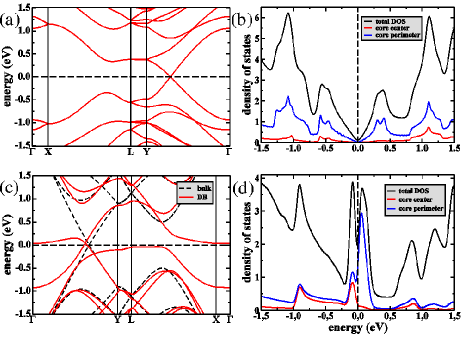
In the case of GB’s in graphene, the electronic structure has been amply discussed in Ref. jsa, , where the occurrence of an anisotropic Dirac cone in a Brillouin-zone (BZ) line along the GB direction was analyzed. In Ref. jsa, , the GB electronic states near the Fermi level (FL) were found to disperse in all directions, indicating hybridization with bulk states. Further indication of such hybridized nature of GB states is provided by the analysis of the full band structure and density of states (DOS) of the GB supercell. Figure 2(a) shows the band structure along the BZ lines shown in Fig. 1(f). Note that the states near the Dirac point show sizeable dispersions in directions perpendicular to the defect (Y-M and -X lines). The contributions of the orbitals centered on the atoms at the GB core to the resonances introduced in the DOS of graphene are shown in Figure 2(b). For the purpose of our analysis, we define the core of both the GB and DB558 defects as composed by the ten atoms that form the topological defects along the defect line, as indicated in Fig. 1. In the DOS plots, we refer to atoms 1 and 2, that are placed along the line at the geometric centers of both defects, as core center, while the remaining eight core atoms are referred to as core perimeter. In the case of the GB, the contribution of the ten core atoms to the four DOS peaks near the FL ranges from 41% to 57%. These results will be contrasted with the case of the DB558 in the following.
The band structure and the DOS for the DB558 are shown in Fig. 2(c) and (d), respectively. In Fig. 2(c) we also include the band structure of a 64-atom bulk supercell, obtained by removing core atoms 1 and 2 from the geometry in Fig. 1(a). Given the periodicity of both defect and bulk cells along the DB558 direction (a zigzag direction of the bulk matrix), the Dirac point of the bulk cell folds onto the point at , where is the period of the DB558 nakada . Note that, to a large degree, the changes in the DB558 band structure with respect to the bulk one are concentrated in a region of from the FL, and that within 0.2 eV above (below) the FL we find bands with flat sections along the Y (L-X) direction (both parallel to the defect line). These states show little or no dispersion along the -X and Y-M lines that are perpendicular to the defect line. The flat-band character of the states above the FL, near the zone center, leads to a ferromagnetic state for a bulk 1D defect in graphene consisting entirely of carbon atoms, as discussed below.
Considering now the DOS for the DB558 in Fig. 2(d), we find two sharp resonances within 0.1 eV from the FL, associated to the 1D defect. These resonances reflect the presence of extended van Hove regions in the in the bandstructure, as seen in Fig. 2(c). We observe that in one feature the DOS of the DB558 differs markedly from the GB one: the peak just above the Fermi level shows a very strong concentration on the core atoms, with 80% of the total DOS concentrated on the orbitals centered on the perimeter core atoms numbered 3, 4, 5, and 6, along the zigzag chains that bond to the dimers (atoms 1 and 2) at the core center in Fig. 1(b). Adding the contributions of the atoms from the same sublattice as atoms 3-6, in the zigzag chains nearest to the core on both sides of the defect line, we already account for 96% of the total DOS for this peak. A strongly one-dimensionally confined empty state along the defect core is thus a characteristic of the DB558. In our calculations, however, these states are empty in the neutral system, hence no spin polarization is induced.
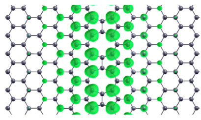
In order to investigate the formation of magnetic states in gate-doped versions of this system, we added one electron per supercell, a doping concentration that raises the FL by about 0.07 eV. A spin-polarized calculation stabilizes a ferromagnetic state, with a magnetic moment of 0.52 per defect unit, and a formation energy that is 40 meV per defect unit lower in energy than the unpolarized state. Figure 3 shows a representative isosurface of the difference between majority and minority spin densities. The spin density is concentrated on the sublattice of the atoms 3-6, with a negligible contribution from the dimer atoms themselves and also from the atoms near the core that belong to the other sublattice. We see here a manifestation of a magnetic state along a line defect that is fully immersed within the bulk of graphene. The fact that these states have a negligible contribution along the dimer atoms is perhaps the origin of the topological disruption in the electronic states that leads to the localization of the related -orbital bands and hence to the magnetic state. We speculate that such DB magnetic states should be more easily detectable experimentally than those predicted to occur along the edges in graphene ribbons nakada ; hlee ; louie3 ; simone , since the zigzag chains along the DB are protected from reconstruction.
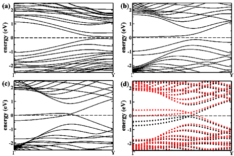
To address the effect of chemical doping on the electronic states of the 1D defects, we considered the oxidized forms shown in Fig. 1. The corresponding band structures are shown in Fig. 4. For both the GB+O and DB55+2O, where oxygen-induced unzipping of the C-C bonds takes place, we observe the opening of small gaps of 55 meV and 190 meV, respectively. In neither of these two cases we find magnetic ground states in the neutral system. An interesting case is the DB558+O system, with one oxygen atom per defect cell, in which the oxygen atom bonds with the two carbon atoms at the defect core in the bridge position. In this case, as shown in Fig. 4(c), the occupied band along the Y line that is 0.1 eV below the FL in the pure DB558 system is now deeper in energy. More importantly, a significant change is observed in the flat band of confined 1D states near that now crosses the FL. As a result, a magnetic ground state is stabilized, with a net magnetic moment of 1.1 per unit cell, as shown in Fig. 4(d), where majority and minority spin bands are plotted. Note that spin-polarization is strongly localized on the 1D defect, with significant exchange splitting restricted to the quasi-1D bands crossing the FL. This ferromagnetic ground-state is 43 meV (per defect unit) lower in energy than the non-polarized state. This value is very close to that for the pure DB558 system with an extra electron per cell. Hence, chemical doping offers another way of stabilizing this ferromagnetic state. The ferromagnetic instability of these flat-band states is further confirmed by a calculation we performed for the DB558+2O system with an extra charge added to the defect supercell. Again, the FL shifts into the band of quasi-1D states, and the system stabilizes a ferromagnetic state. Just as in the case without O doping, the presence of extended van Hove regions is also clearly seen in the band structures in Fig. 4.
We turn our attention now to the charge transfer between the 1D defects and the surrounding graphene bulk, since this may give important qualitative information about the nature of the scattering of charge carriers by such 1D defects. In Fig. 5, we show the profile of the charge distribution around the 1D defects, and the integrated charge per atom, both as a function of the distance to the geometric center of the defect, for the DB558 and the GB. The charge distribution is shown as linear charge densities representing the net charge summed over atoms at the same distance from the 1D defect, divided by the period of the defect unit. The integrated charge is the integral of this linear charge density profile, computed as total net charge per atom, and defined as follows:
| (1) |
where is the linear charge density for the line of atoms at a distance from the defect, is the period of the 1D defect, and is the number of atoms summed over all lines with .
Figure 5 shows that the charge redistribution around the 1D defects is non-monotonic, with the linear charge distributions alternating in sign on both sides of the defect, as seen in Fig. 5(a). Note also that charge transfer between the 1D defects and the graphene matrix occurs in a range of 3-5 Å from the defect line, with the graphene matrix becoming neutral beyond this range, as shown in the plots for in Fig. 5(b). Since the charge distribution region recovers neutrality within 3-5 Å from the defect center, we expect no long range Coulomb scattering of charge carriers from both 1D defects. In our calculations, oxidation of the 1D defects is found not to affect this localized character of the charge balance between the defects and the graphene bulk. Such extended 1D defects should then play a minor role as a source of carrier scattering in graphene.
In summary, we find that the electronic states introduced by grain boundaries in graphene are only partially confined to the defect core, while a domain boundary introduces unoccupied electronic states near the Fermi level that are very strongly confined to the core of the defect, and that, when populated by doping, display a ferromagnetic ground state in a 1D defect that is fully contained within the bulk matrix and that consists entirely of carbon atoms. Being fully bulk-immersed, this ferromagnetic state is protected from reconstruction and should be more easily detectable experimentally than those predicted to exist along the edges of graphene ribbons. Furthermore, our calculations indicate that charge transfer between bulk graphene and both types of extended 1D defects is strongly localized, with charge redistribution confined to 3-5 Å from the geometric center of the 1D defect, implying that these 1D defects should act as weak charge scatterers in graphene.
On leave from Boston University, USA.
Acknowledgements.
SSA, RWN, and ALD acknowledge support from Brazilian agencies CNPq, FAPEMIG, and Instituto do Milênio em Nanociências-MCT. AHCN thanks the financial support of the NRF-CRP award Novel 2D Materials with Tailored Properties: Beyond Graphene (R-144-000-295-282), US/DOE grant DE-FG02-08ER46512, and US/ONR grant MURI N00014-09-1-1063.References
- (1) A. H. Castro Neto et al., Rev. Mod. Phys. 81, 109 (2009), and references therein.
- (2) J. Lahiri et al., Nature Nanotech. 5, 326 (2010).
- (3) Q. Yu et al., Nature Mat. 10, 443 (2011).
- (4) M. U. Kahaly, S. P. Singh, and U. V. Waghmare, Small 4, 2209 (2008).
- (5) J. da S. Araújo and R. W. Nunes, Phys. Rev. B 81, 073408 (2010).
- (6) P. Simonis et al., Surf. Sci. 511, 319 (2002).
- (7) J. Cervenka and C. F. J. Flipse, Phys. Rev. B 79, 195429 (2009).
- (8) O. V. Yazyev and S. G. Louie, Phys. Rev. B 81, 195420 (2010).
- (9) D. Gunlycke and C. T. White, Phys. Rev. Lett 106, 136806 (2011).
- (10) X. Lin and J. Ni, Phys. Rev. B 84, 075461 (2011).
- (11) C. Gómez-Navarro et al., Nano Lett. 10, 1144 (2010).
- (12) A. Bagriet al., Nature Chem. 2, 581 (2010).
- (13) N. M. R. Peres, F. Guinea, and A. H. Castro Neto, Phys. Rev. B 73, 125411 (2006)
- (14) A. H. Castro Neto, C. de C. Chamon and C. Nayak, Phys. Rev. Lett. 79, 4629 (1997).
- (15) A. Ferreira et al., EPL 94, 28003 (2011).
- (16) W. Kohn and L. J. Sham, Phys. Rev. 140, A1133 (1965); J. P. Perdew, K. Burke, and M. Ernzerhof, Phys. Rev. Lett. 77 3865 (1996).
- (17) N. Troullier and J .L. Martins, Phys. Rev. B 43, 1993 (1991); L. Kleinman and D. M. Bylander, Phys. Rev. Lett. 48, 1425 (1982).
- (18) J. M. Soler et al., J. Phys. Cond. Matt. 14 2745 (2002).
- (19) K. Nakada, M. Fujita, G .Dresselhaus, and M .S. Dresselhaus, Phys. Rev. B 54, 17954 (1996);
- (20) H. Lee, Y. W. Son, N. Park, S. Han, and J. Yu, Phys. Rev. B. 72, 174431 (2005).
- (21) Y. W. Soon, M. L. Cohen, and S. G. Louie, Nature 444, 347 (2006).
- (22) S. S. Alexandre, M. S. C. Mazzoni, and H. Chacham, Phys. Rev. Lett 100, 146801 (2008).