The Difficulty of Gate Control in Molecular Transistors
Abstract
The electrostatic gating effects on molecular transistors are investigated using the density functional theory (DFT) combined with the nonequilibrium Green’s function (NEGF) method. When molecular energy levels are away from the Fermi energy they can be linearly shifted by the gate voltage, which is consistent with recent experimental observations [Nature 462, 1039 (2009)]. However, when they move near to the Fermi energy (turn-on process), the shifts become extremely small and almost independent of the gate voltage. The fact that the conductance may be beyond the gate control in the “ON” state will challenge the implementation of molecular transistors.
pacs:
73.63.-b, 85.65.+h, 85.30.TvIntroduction. — The molecular transistor is the most essential element of molecular electronics. How to control molecular orbitals by external gate voltage () is the key problem of molecular transistors. Although two-terminal molecular devices (with the source and drain electrodes) have been extensively studied for many years, the real three-terminal ones (with the gate electrode added in) have only been developed recently in the laboratory by Song et al Son09 . They found that the transport current of Au/1,4-benzenedithiol (BDT)/Au (as well as Au/1,8-octanedithiol/Au) in a transistor structure can be directly controlled by gate modulating molecular orbitals. A linear relationship between the gate voltage and the shift of the molecular orbital energy has been also observed Son09 . Based on their experiment, it seems that the practical molecular field-effect-transistor (FET) will be realized soon.
From a practical point of view, in order to control the carriers or the "conductive channel" by the gate voltage, the molecular FET should work well on three modes of operation (as the traditional counterpart does): cutoff, linear and saturation regions. We comment that the gate control of molecular orbital only observed in the cutoff region, i.e. the channel between the source and drain keeping in the “OFF” state in the experiment Son09 . Of course, one expects molecular-orbital-gating occurring in the cutoff region is also valid in the other two regions (the “ON” states). However, such natural extrapolation in micro electrons is questionable in molecular transistors, because at the molecular level the motion of carriers obeys quantum mechanical which may make the real situation completely different. In this letter, we will address this issue via the first principles calculations–the density functional theory (DFT) combined with the nonequilibrium Green’s function (NEGF) method. We will demonstrate that above extrapolation does be problematic: once the channel between the source and drain being turned on, the conductance of the molecular transistor may be beyond the control of gate voltage. This may be a serious challenge to the implementation of molecular transistors.
Method. — The gate-controlled Au/BDT/Au structure is the object of our theoretical study. However, the aim of the present work is not to quantitatively simulate the experment of Song et al , but to qualitatively reveal the physics behind it and the physics being missed in it. Based on this point, we apply the gate voltage via an additional external potential instead of adding a real gate electrode in the first principle calculations (the latter is very difficult for DFT+NEGF calculations).
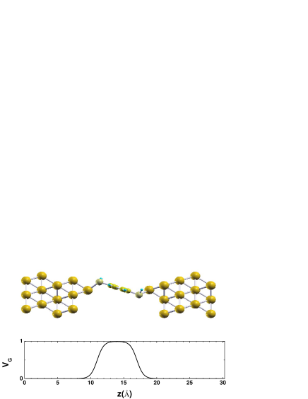
The Au/BDT/Au structure consists three parts: the left and right electrodes plus the scattering region (with gate voltage being applied). Both of the electrodes are periodically repeated structures of the super cell formed by 3 layers of 33 Au(111) slabs, while the scattering region is composed of a single molecule BDT and four layers of 33 Au(111) slabs on each side. The BDT molecule bounds to the electrode surfaces through the thiol groups contacting with Au adatoms on each side, as shown in Figure 1. It is reported that when BDT molecule contacts with Au leads, the structure with the thiol group S-H non-dissociated is energetically more favoriteJi09 ; Strange11 , thus we adopted this kind of structure in our calculation. As in most literatures, BDT molecule is set perpendicular to the Au surfaces. Although the molecule structure and its coupling to the electrodes may change the conductance of BDT single molecular junction, they should not cause qualitatively difference to the results reported here. We will neglect those effects and focus on the gate-controlled conductance of single-structure molecular junctions.
All of the calculations are performed with spin-polarized DFT implemented in the Siesta code siesta1 ; siesta2 using Perdew-Burke-Ernzerhof exchange-correlation functional PBE . Double- plus polarization function(DZP) basis set is used, together with a mesh cutoff of 200 Ry and norm-conserving pseudopotentials. The distance between the left and right lead surfaces is relaxed to the equilibrium position. Then the BDT molecule together with the nearest layer of Au atoms are fully relaxed to fulfill the energy and force convergences of 10-5 eV and 0.01 eV/Å respectively.
The transport property is calculated using DFT+NEGF method implemented in the recent Siesta code (the TranSiesta part Bra02 ). The periodic boundary conditions are used in directions orthogonal to the transport direction. A 33 uniform meshes are sampled over this two-dimensional Brillouin zone. The density is integrated with 32 points on the semicircle, 32 points parallel to the real axis, and 16 poles. The transmission spectrum at zero bias is obtained by integrating over 1000 points.
To study the electrostatic gating effects, we follow the idea of Morari et al., i.e. the gate voltage is simulated by adding external potential determined solely by the coordinate along the transport direction morari09 . In our work, the external potential is in the form of
| (1) |
where Å. The parameters and are used to ensure that the applied gate-potential lies in the molecule region and decrease to zero smoothly when reaching the electrodes, as the potential profile shown in Figure 1. Comparing with experiments, this simulation of gate voltage obviously lacks the effect of the gate dielectric ( layer in Ref.Son09, ). This effect should not distinctly change the physics presented in this work, at least in the qualitatively level.
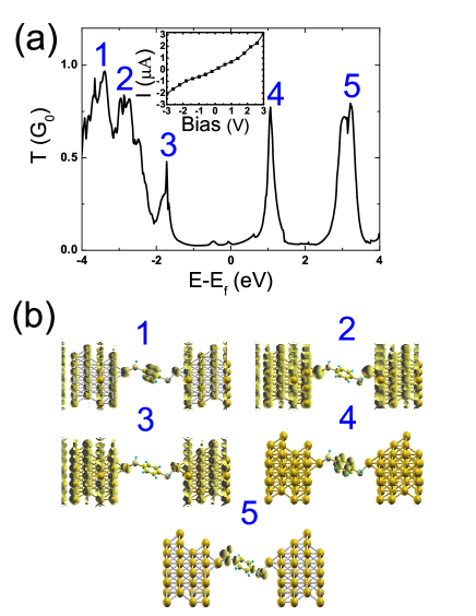
Results and discussions . — We first check our calculation before the gate voltage being applied and the results are summarized in Figure 2, where the upper panel depicts the zero-bias transmission spectrum (the Fermi energy is set as the zero point of energy), with its insert showing the calculated curve. One can see that the current is of the same order () with experimental measurement Son09 , which is apparently an acceptable result for static DFT. It further confirms the chosen junction geometry (see Figure 1) is reasonable. The asymmetric character of curve is also consistent with experiment Son09 , which may result from the asymmetric coupling of BDT molecule with the left and right electrodes.
From Figure 2, we find five transmission peaks within the energy range of to eV and they are labeled as peaks 1-5, where peaks 1-3 (centered on , and eV respectively) correspond to hole-transport while peaks 4-5 (centered on and eV respectively) to electron-transport. Actually, we can further identify which element (C, S or Au) contributes most to those peaks via the spatial charge density [also called the local density of states (LDOS)] within energy ranges around them, as shown in the lower panel of Figure 2. It can be seen that C atoms contribute most to both peaks 1 and 4, while Au atoms (including those linking BDT and bulk electrodes) do most to peaks 2 and 3. The main contribution to peak 5 is clearly from S atoms and the S-C hybridization. From those information, we can conclude that peaks 1 and 4 are respectively result from the conduction of the highest occupied molecular orbital (HOMO) and lowest unoccupied molecular orbital (LUMO) of BDT. Since the LUMO is nearest to , it will dominate the transport properties of the device under low bias voltage. This result seems not consistent with the experiment of Song et al, where the HOMO is observed to be turned on prior to the LUMO. It indicates that some factors may be missed in our ideal DFT calculations, e.g. many body corrections Strange11 . We argue that the physics of activating and controlling LUMO or HOMO should be same for molecular transistors 111Actually, that point has been proved by Song et al in their experiment, e.g. see the Supplementary Fig. 8 of Ref.Son09, . In the present paper, the evidence is shown in Figure 3(b). .
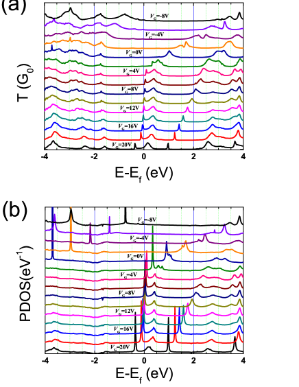
Now, let us show the complete story when gate voltage being applied in the form of Eq.(1) (cf. Figure 1). In Figure 3(a), we plot the transmission spectrum under various gate voltages (from V to V with the interval of V). As we have demonstrated in Figure 2, the LUMO of BDT plays the leading role in the molecular-orbital-gating process under low bias. It should be enough for us to focus on the gate control of this orbital, e.g. the change of transmission peak 4 with . To be more specific, Figure 3(b) depicts the projected density of states (PDOS) only on carbon atoms (to highlight the change of LUMO) under synchronously changing as shown in Figure 3(a). Combining Figure 3(a) and 3(b), we can clearly see the modulation of on the energy of the LUMO () and accurately understand its mechanism.
At first glance, Figure 3 does confirm the fact that the conductance and molecular orbital of BDT junction can be directly controlled by . However, in different range of , molecular-orbital-gating exhibits different behavior patterns. Generally speaking, Figure 3 [both (a) and (b)] can be divided into three regions in term of , which are explained in details as follows.
Region I (): In this region, the molecular transistor is in the “OFF” state due to the near zero DOS and near zero at . Actually, it is the region where Song et al observed molecular-orbital-gating in their experiment Son09 . Our theoretical results verify their observation that the gate control of molecular orbital is linear and effective. To demonstrate this point in more details, we extract the change of the energy of the LUMO (defined as ) as functions of from Figure 3 (in all range of , not only in Region I), and summarize the results in Figure 4. In that figure, the remarkable linear-modulation of on is clearly shown in region I, with the slope being defined as the gate efficiency factor, (cf. Ref.Son09, ). From Figure 4, we work out in Region I.
By referring 3(b), one can find a similar linear-control of on the energy of the HOMO () in the energy range of . The gate efficiency factor, , is the same as that of gate control of in spite of a sign difference. That result confirms our argument that activating and controlling LUMO or HOMO should share the same physics. Not surprisingly, the activation of the HOMO is much harder than that of the LUMO in our theory.
Our theoretical ) is comparable with the experimental value Son09 . That provides a reliable basis for further understanding theoretical results in Region II, which has not been reported in experiments yet.
Region II (): In this region, the molecular transistor is in the “ON” state due to the finite DOS and finite at . As shown in Figure 3 and 4, the behavior of molecular-orbital-gating in this region is completely different from that in Region I: both DOS and near change very slowly with further increasing once the LUMO has been activated to be conductive. If we still linearly fit the gate modulating on in Figure 4, we will get a near zero (). It indicates that the energy of LUMO becomes beyond the control of gate voltage in this region.
The weak dependence of on means the source-drain current at finite bias also independent on , i.e. will lose the control of in molecular transistors in the “ON” state. That will challenges the implementation of molecular transistors. As we know, at certain source-drain bias () is supposed to increase with linearly in the linear region and quadratically in the saturation region. Neither of them can be achieved when the molecular orbital being beyond the control of .
In order to gain an insight into the difficulty of gate control in Region II, we show the planar-averaged converged Hartree potentials () under various in the insert of Figure 4, where the peaks correspond to chemical bonds while the valleys to chemical groups (CH or SH) or Au atoms. By comparing Figure 4 and Figure 1, we find two potential nodes at the interface between BDT and Au electrodes (S-Au bonds). The potential of S atoms inside the nodes drops rapidly with increasing , while that of Au atoms outside of the nodes grows fast.
Since negative potential tends to trap electrons but positive one trap holes, those two nodes indicate that -induced negative and positive charges localized at the interfaces separates from each other (see Table I for further details). As a consequence, an inner electric field builds up to offset the -induced one. This process is very similar to the shielding of external field by a plate capacitance, we thus called the effective capacitance near the (left or right) interface as structural capacitance (). It can explain why the effective potential acting on molecular energy is less than the applied one (), even no gate dielectric structure being included.
| -8 | -4 | 0 | 4 | 8 | 12 | 16 | 20 | |
|---|---|---|---|---|---|---|---|---|
| 0.09 | 0.04 | 0 | -0.03 | -0.07 | -0.11 | -0.16 | -0.21 | |
| -0.13 | -0.06 | 0 | 0.08 | 0.18 | 0.27 | 0.37 | 0.46 | |
| 0.11 | 0.05 | 0 | -0.06 | -0.11 | -0.17 | -0.23 | -0.29 | |
| -0.16 | -0.07 | 0 | 0.08 | 0.18 | 0.29 | 0.40 | 0.50 | |
| Total | 0.67 | 0.32 | 0 | -0.41 | -0.94 | -1.48 | -2.02 | -2.54 |
When the molecular transistor is in the “ON” state, the finite DOS at [] will lead to the so called quantum capacitance effects QC ; Datta . The quantum capacitance can be defined through . In a realistic transistor, the effective capacitance is the series combination of the electrostatic capacitance () and . In our theory, is replaced by structural capacitance , therefore, , which is obviously dominated by the smaller of the two. As shown in the insert of Figure 4, the narrow distance between opposite charges indicates that should be very large (plate capacitance model), which makes dominate. As a consequence, effectively reduces the external potential acting on BDT, or even completely shield -induced field to make loss control of molecular orbitals.
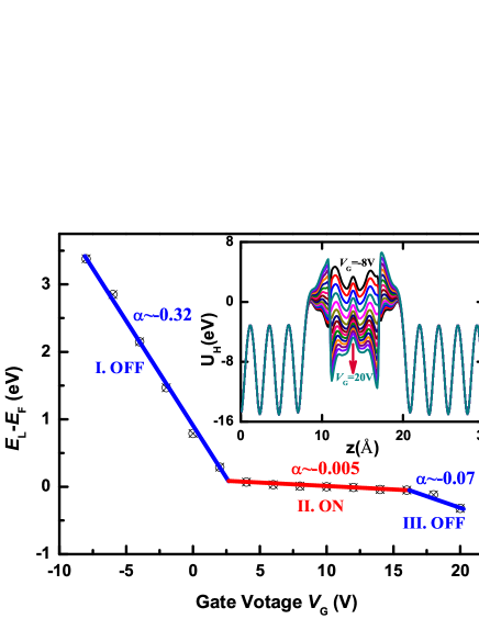
Region III (): The molecular transistor is turned back to “OFF” state when sufficient large shifts the LUMO of BDT away from . The efficient linear-modulation of on molecular orbitals is also restored but with a different slope () from that in Region I. When the LUMO+1 of BDT is shifted near , one can expect a similar process as happens in Region II. In that case, the electron-electron correlation should be carefully treated (beyond the mean-field theory) due to more electrons being trapped within the BDT molecule, which has been already beyond the scope of the present work.
Summary. — In summary, we have studied the gate control of molecular orbitals by DFT+NEGF method. When molecular energy levels are away from the Fermi energy they can be linearly shifted by the gate voltage, which is consistent with recent experimental observations. When they move near to the Fermi energy, the shifts become extremely small and almost independent of the gate voltage, which indicates that it may be difficult for the gate voltage to control molecular orbitals in the “ON” state.
Acknowledgements.
Support from NSFC of China (Grant No. 11074303) are gratefully acknowledged. Part of the computer time is supported by Physics Laboratory for High Performance Computing, Renmin University of China.References
- (1) H. Song, Y. Kim, Y. H. Jang, H. Jeong, M. A. Reed and T. Lee, Nature (London) 462, 1039 (2009).
- (2) Z. Ning, W. Ji, and H. Guo, arXiv:0907.4674.
- (3) M. Strange, C. Rostgaard, H. Häkkinen, and K. S. Thygesen, Phys. Rev. B83, 115108 (2011)
- (4) P. Ordejon, E. Artacho and J.M. Soler, Phys. Rev. B53, R10441 (1996).
- (5) J.M. Soler, E. Artacho, J.D. Gale, A. Garcia, P. Junquera and P. Ordejon, J. Phys.: Condens. Mater 14 , 2745 (2002).
- (6) J.P. Perdew, K. Burke and M. Ernzerhof, Phys. Rev. Lett. 77, 3865 (1996).
- (7) M. Brandbyge, J.L. Mozos, P. Ordejón, J. Taylor and K. Stokbro, Phys. Rev. B65, 165401 (2002).
- (8) C. Morari, I. Rungger, A.R. Racha, S. Sanvito, S. Melinte and GM. Rignanese, ACS Nano 3 , 4137 (2009).
- (9) S. Luryi, Appl. Phys. Lett. 52 , 501 (1988).
- (10) S. Datta, Quantum Transport: Atom to Transistor, Cambridge Univ. Press, 2005.