Concept and status of the CALICE analog hadron calorimeter engineering prototype
Abstract
A basic prototype for an analog hadron calorimeter for a future linear collider detector is currently being realized by the CALICE collaboration. The aim is to show the feasibility to build a realistic detector with fully integrated readout electronics. An important aspect of the design is the improvement of the jet energy resolution by measuring details of the shower development with a highly granular device and combining them with the information from the tracking detectors. Therefore, the signals are sampled by small scintillating tiles that are read out by silicon photomultipliers. The ASICs are integrated into the calorimeter layers and are developed for minimal power dissipation. An embedded LED system per channel is used for calibration. The prototype has been tested extensively and the concept as well as results from the DESY test setups are reported here.
1 Introduction
The CALICE collaboration [1] is currently developing a new engineering prototype [2] of the analog hadron calorimeter (AHCAL) option for a future linear collider (LC) experiment. A major aspect of the design is the improvement of the jet energy resolution by measuring details of the spatial development of all hadronic showers inside a jet. These information are combined with the information obtained from the tracking systems in order to measure only the energies of neutral particles with the calorimeter system. This concept is known as particle flow and has been validated [3] with the physics prototype [4] of the CALICE AHCAL. The aim of developing an engineering prototype is to demonstrate that a scalable device can be built that meets the reqirements of a realistic LC detector, such as fully integrated front-end electronics in the active layers of the calorimeter. It is based on scintillating tiles, that are read out by silicon photomultipliers (SiPMs).
First subunits (HCAL base unit, HBU) with 144 detector channels of size cm2 have been produced and extensively tested in the laboratory as well as in the DESY test beam facility [2, 5, 6]. They include the scintillating tiles, four front-end low power dissipation SPIROC2 ASICs [7] and the light calibration and gain-monitoring system. The first version of the detector/DAQ interface modules is used for power supply and slow control programming. For studying a realistic LC operation mode the power supply module allows for switching off individual detector components within the LC bunch train structure (power pulsing) [8].
Recently all sub-components of the HBU (tiles, ASICs, calibration system) as well as the DAQ modules have been redesigned in order to optimize the performance and the spatial dimensions. First tests have been performed with the next generation SPIROC2b ASIC [9]. In this report the concept and the status of the design as well as results from test measurements are presented.
2 Design and status of the engineering prototype
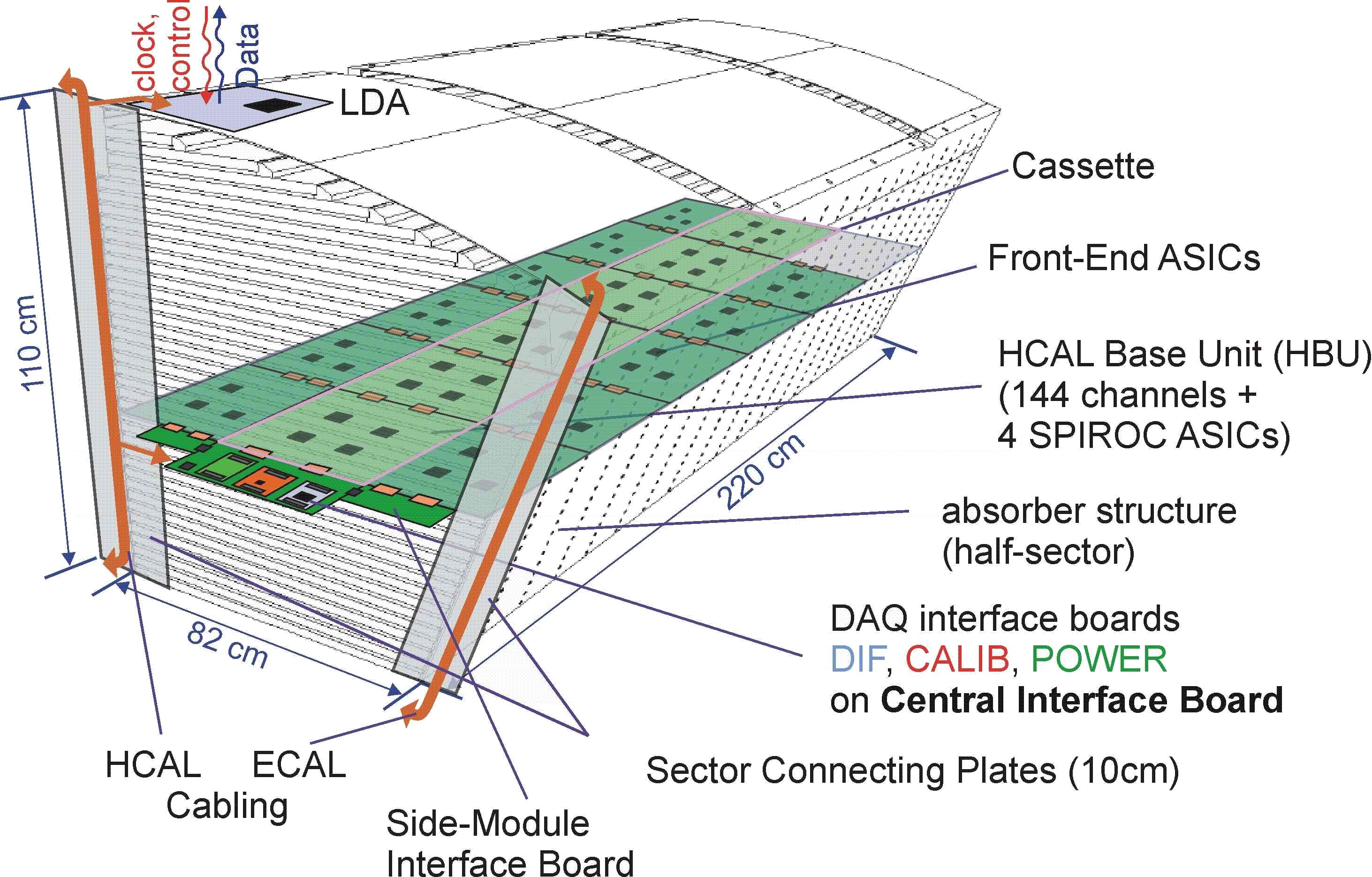
The design of one half-octant of the AHCAL is shown in Fig. 1. It consists of 48 layers, giving a total thickness of 110 cm. The barrel is divided into two sections, which have a length of 220 cm each. One layer consists of the 16 mm thick stainless steel or 10 mm thick tungsten absorber plate and an active layer part. This active part consists of the scintillating tiles with an attached SiPM as photo detector and the embedded front-end electronics with the readout chips and the calibration system. Each layer has about 2500 channels, which adds up to about 4 million channels for the whole barrel calorimeter.
2.1 HCAL base units
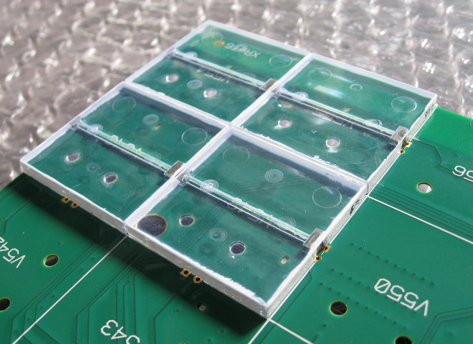
A single layer is divided into three parallel slabs, each of which consists of six HBUs that are interconnected by ultra-thin flexleads. The first version of the HBU has been tested extensively at DESY with charge injection and LED light as well as in the DESY electron test beam environment [2]. It features 144 detector channels of cm2 size. The signal for each channel is produced by a scintillating tile with 3 mm thickness, that includes a straight wavelength shifting fiber coupled to a SiPM with a size of 1.27 mm2 on one side and to a mirror on the other side. The SiPM comprises 796 pixels with a gain of . The tiles are connected to the PCB by two alignment pins that are plugged into holes in the PCB, while the nominal tile distance is 100 m. A photo of the actual tile assebly is shown in Fig. 2.
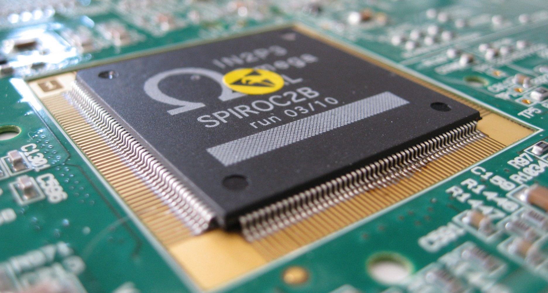
The analog signals of the SiPMs are read out by 36-channel ASICs [7] equipped with 5 V DACs for channel-wise bias voltage adjustment. They provide two gain modes, where the high gain mode is maily used as a calibration mode and the low gain mode measures signals with higher amplitudes up to SiPM saturation. The foreseen power consumption amounts to 25 W (40 W) per channel (including SiPM bias) for the final LC operation in order to avoid the need for active cooling. This means that parts of the chip have to be switched off according to the bunch train structure of the LC to save power. First tests of the performance of the power pulsing mode in a full HBU setup have been performed with the SPIROC2 chip, which gave good results [8]. The ASICs include the digitization step (12-bit ADC and 12-bit TDC for charge and time measurement) and the on-detector zero suppression with an adjustable threshold. This self-triggering capability has been extensively tested in the DESY test beam environment [5]. Additionally, the chip can automatically chose between high gain and low gain channel, which is described in Sec. 3.3. To reduce the height of the active layers the ASICs are lowered into cutouts of the PCB by 500 m. Recently a new version of the ASIC, the SPIROC2b, has become available, mounted on the first version of the HBU and first tests have been performed. A photo of the new chip as it is integrated into the HBU is shown in Fig. 3.
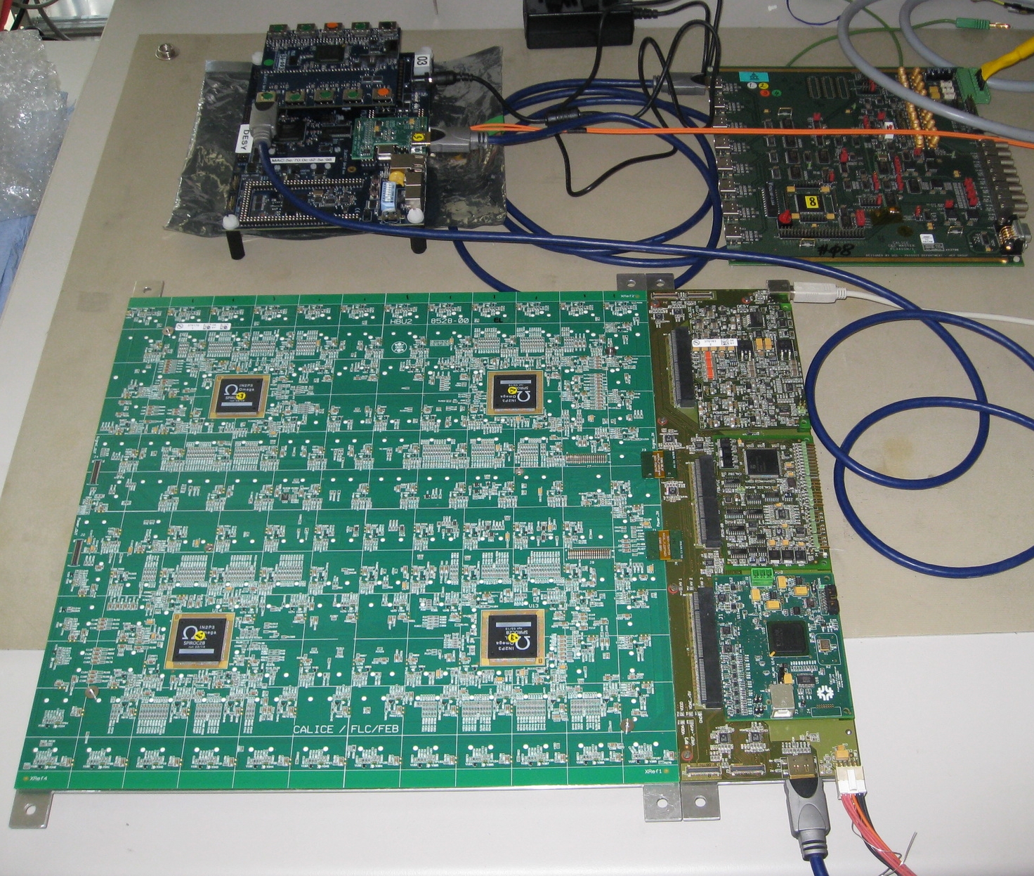
A second version of the HBU has been produced (using the SPIROC2b chip) and first tests of its functionality have started. It has an optimized electronics design and especially the implementation of the calibration system has been updated. Figure 4 shows the new HBU as it is connected to the DAQ interface modules (see Sec. 2.3).
2.2 Calibration system
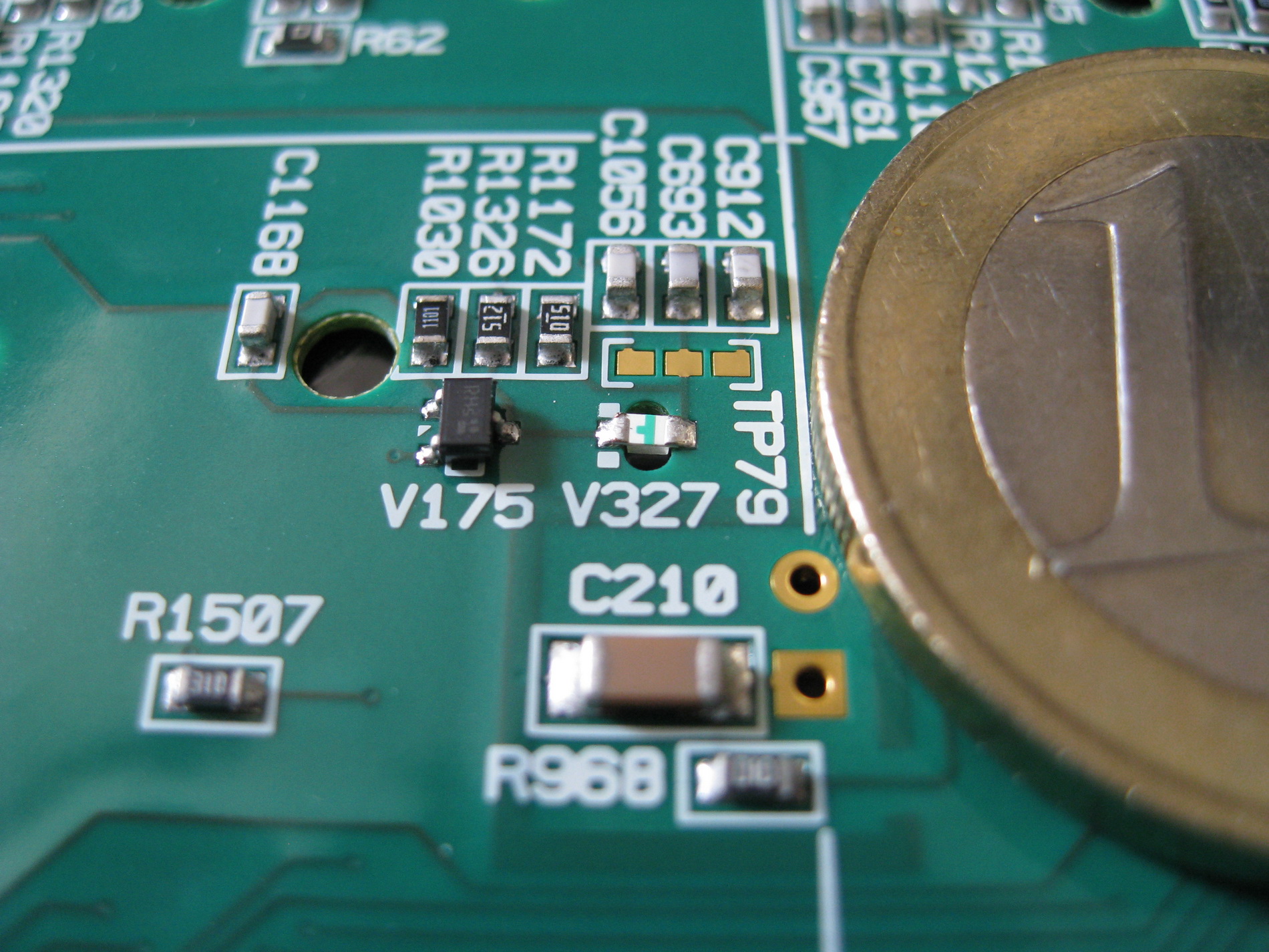
The response of the SiPM is strongly temperature and bias voltage dependent and it saturates for high light intensities due to the limited number of pixels. Therefore, a gain-calibration and saturation-monitoring system with high dynamic range is needed. For the gain calibration a low light intensity is used to measure the gain of the photo detector from the distances of individual peaks in a single-pixel-spectrum, while for high light intensities, that correspond to 100 minimum-ionizing particles, the SiPM saturates. Two concepts are currently under under study:
-
1.
Each channel features an integrated LED, that is reverse mounted into a hole in the PCB and shines on the tile. This system is used in the HBUs in the DESY test setups, see Fig. 5.
-
2.
Few strong LEDs that are placed on a special board outside the detector, while the light is distributed via notched fibers [10].
Both options have been tested successfully in the DESY test beam environment. For the design of the new HBUs the driver circuit of the integrated LED system has been optimized in order to achieve optical pulse lengths of about 10 ns for a wide range of amplitudes. This is needed to provide a good quality for the single-pixel-spectra that can be evaluated in the gain calibration procedure with high efficiency. UV LEDs have been used for this purpose, while the option of blue LEDs is kept for future developments. It has also been shown that the light intensity of the UV LEDs for a bias voltage of up to 10 V is high enough to saturate the SiPMs. In order to minimize the number of calibration runs in test beam operations, it is important to have a reasonable uniform light output for a large sample of LEDs. This is achieved by using an array of different LED loading capacities that can be chosen individually channel by channel, since all channels have a common LED bias voltage.
2.3 Data acquisition interface
As can be seen in Fig. 1, each slab of HBUs is connected to a DAQ system at the end of each layer [2]. The Central Interface Board (CIB) hosts the Detector Interface (DIF), the steering board for the calibration system (CALIB) and the power module (POWER), that distributes all voltages needed in the slab. The DIF serves as the interface between the inner-detector ASICs and the DAQ. The middle slab in each layer is directly connected to the CIB via flexleads, while the side slabs are connected to the CIB via side interface boards (SIBs). There are currently two options for the operation of the DAQ system. For laboratory tests a USB interface is used that connects the DIF directly to a PC, where a Labview based user interface is running. This interface has been used for the measurements presented later in this report. For the operation of a larger detector a more advanced DAQ system is needed that uses the Link/Data Aggregator (LDA, also shown in Figs. 1 and 4) that collects the data from the DIFs to send them via an optical link to the DAQ PCs and the Clock and Control Card (CCC) that provides the common clocks for all components. All modules are available at DESY and are currently under test to commission the communications between the different systems. Figure 4 shows the complete DAQ setup as it is currently used at DESY, including the new HBU, the CIB, the LDA and the CCC with all interconnections.
3 Measurements and results
The main task of the current tests is to commission the detector concept for a larger scale prototype. The functionality of the ASICs and tiles in the HBU environment has been proven in laboratory and test beam measurements for the first version of the HBU [2]. Since then many subcomponents have been further developed and their tests are an ongoing task. Three examples are reported here.
3.1 Tiles
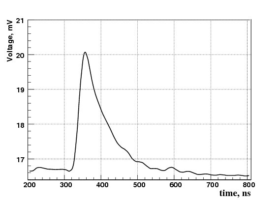
For the equipment of the new HBUs a new generation of tiles with SiPMs is developed. A first sample of 20 tiles has been tested at DESY by measuring the gains and pulse shapes [6]. Therefore, the optimal bias voltage as indicated by ITEP has been applied to each SiPM and light pulses with differing amplitudes from blue LEDs were used to illuminate them. A typical pulse shape as measured with a QDC directly at the output of the SiPM is shown in Fig. 6. The mean value of the pulse lengths, defined as the widths of the signals at 10% of the maximal amplitude, is 219 ns, while the distribution ranges from 120 ns to 320 ns [6].
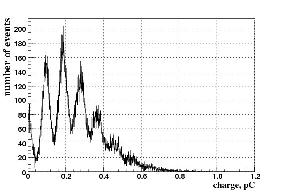
As discussed in Sec. 2.2, the gain of each SiPM can be calibrated by measuring a single-pixel-spectrum. All tested tiles could be calibrated with charge integration times between 50 ns and 160 ns. Note that the SiPM signal is passed through a shaper with 50 ns shaping time in the ASIC and that this corresponds to roughly 100 ns integration time when using a QDC. A typical single-pixel-spectrum is shown in Fig. 6. The measured gains vary from to , defined for an integration time of 160 ns. Assuming an integration time of 50 ns the gain is a factor of 2.6 smaller [6]. A larger sample of tiles will be needed and tested in the near future when the new HBUs have to be fully equipped.
3.2 First SPIROC2b measurements in HBU environment
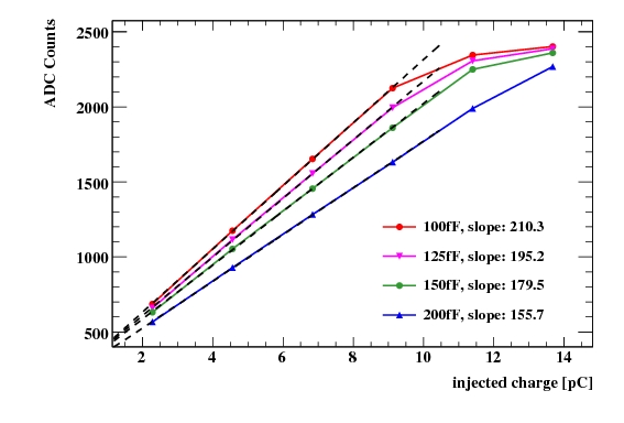
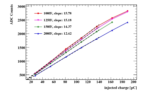
The SPIROC2b is the latest version of the SPIROC chip family and has been mounted on the first version of the HBU for first system tests. The preamplifier gain can be adjusted individually for every readout channel in order to compensate fluctuations in the photo detector gain. The preamplifier feedback capacitance can be varied in the range between 25 fF and 1575 fF in steps of 25 fF, while the ratio of the high gain and low gain amplifications is fixed to 10. The linearity and the overall behaviour has been tested with charge injection for multiple channels and multiple values for the capacitors. It is expected that a value between 100 fF and 200 fF is optimal for efficient use of the dynamic range of the ADC in the low gain channel. At the same time it is important to get a reasonable resolution in the high gain channel to measure single-pixel-spectra for the calibration of the photo detector gain.
Figure 7 shows the measurements of the amplitude in ADC tics as a function of the injected charge, performed for one example channel in high gain mode and different settings for the preamplifier gain. The chip is well linear up to injected charges of around 12 pC. It has to be noted that the ratios between the slopes of the linear fit functions and between the corresponding feedback capacitances are not equal. Figure 7 shows the same measurement for the low gain channel. Again, good linearity can be observed for the whole dynamic range of the ADC.
3.3 Auto-gain
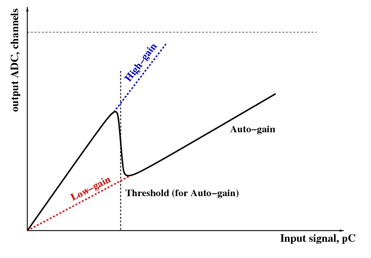
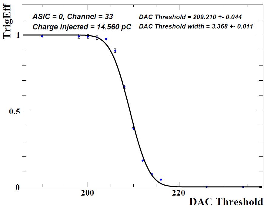
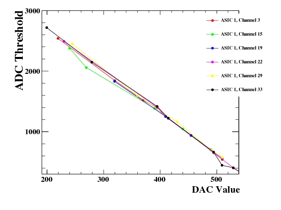
The SPIROC ASIC can chose the gain channel automatically by comparing the signal output from a fast shaper to a predefined threshold, which is set by a 10-bit DAC. If the signal exceeds the threshold, the amplitude measured in the low gain channel of the chip is stored in the data, otherwise the amplitude measured in the high gain channel is stored. An additional bit gives the information about the chosen channel. Fig. 8 shows a schematic drawing of the auto-gain functionality, which has been tested extensively at DESY with charge injection and LED light for the SPIROC2 ASIC [6]. It is expected that the auto-gain efficiency curve, extracted from a threshold scan at a fixed input charge, has a non-zero width. One example measurement is shown in Fig. 9. The amount of injected charge corresponds roughly to the beginning of the high gain saturation region, i.e. the region where a switching from high gain mode to low gain mode is desirable. The width of the efficiency curve in this region corresponds to approximately two photo electrons, which is sufficiently narrow. The amplitude of the threshold as a function of the DAC value has also been measured in order to test the dynamic range of the DAC, which is displayed in Fig. 9. The maximal threshold that can be set by the DAC corresponds to an injected charge of approximately 20 pC, which is well in the saturation region of the high gain mode. Since no significant shifts or non-linearities of the auto-gain mode are observed [6], it can be used in future test beam measurements.
4 Summary and outlook
The CALICE collaboration is currently developing an engineering prototype of an AHCAL for a future LC experiment. It is foreseen to build a full detector layer with a realistic readout scheme, including integrated front-end electronics and a new DAQ system to demonstrate the feasibility and scalability of the concept. A first version of the setup has been tested extensively with charge injection, LED light and electron beams. All results obtained with this setup show very good results in terms of functionality and performance and lead to an ever increasing understanding of the system. As an example, the performance of the auto-gain selection capability has been discussed in this report.
In order to further develop the prototype, all relevant subcomponents have been redesigned, including scintillating tiles, ASICs, HBUs, the LED calibration system and the detector/DAQ interface modules. A second version of the system has been build and the status has been presented here. First measurement results for the SPIROC2b ASIC have been discussed and all tests with charge injection performed so far show good results.
Two of the most important next steps are the further development of the new DAQ system and the commissioning of the new HBUs in terms of overall functionality (including power pulsing) and ASIC performance. The new subcomponents have to be tested in detail to reestablish a fully running system. Additionally, the single HBU setup will be extended to a multi-HBU setup. First, a full calorimeter layer with a length of 6 HBUs will be tested and finally a multi-layer stack will be constructed. A possible application is the detailed measurement of the time structure of hadronic showers.
5 Acknowledgements
The author gratefully thanks Erika Garutti, Peter Göttlicher, Oskar Hartbrich, Mathias Reinecke, Felix Sefkow and Ivan Tolstukhin for very useful discussions and valuable contributions to the results presented here.
References
- [1]
References
- [1] CALICE home page: https://twiki.cern.ch/twiki/bin/view/CALICE/CaliceCollaboration
- [2] M. Reinecke et al., Integration Prototype of the CALICE Tile Hadron Calorimeter for the International Linear Collider, Proc. 2008 IEEE Nuclear Science Symposium (NSS08), NSSMIC.2008.4774800; P. Göttlicher for the CALICE collaboration, First Results of the Engineering Prototype of the CALICE Tile Hadron Calorimeter, Proc. 2009 IEEE Nuclear Science Symposium (NSS09), NSSMIC.2009.5402334; R. Fabbri for the CALICE collaboration, CALICE Second Generation AHCAL Developments, Proc. 2010 LCWS, arXiv:1007.2358; M. Terwort for the CALICE collaboration, Realization and Test of the Engineering Prototype of the CALICE Tile Hadron Calorimeter, Proc. 2010 IEEE Nuclear Science Symposium (NSS10), NSSMIC.2010.1550767.
- [3] C. Adloff et al., Tests of a Particle Flow Algorithm with CALICE Test Beam Data, JINST 6 (2011) P07005, arXiv:1105.3417.
- [4] C. Adloff et al., Construction and commissioning of the CALICE analog hadron calorimeter prototype, JINST 5 (2010) P05004, arXiv:1003.2662.
- [5] J. Rouëné, Analysis of the autotrigger of the read out chip of the front-end electronics for the HCAL of the ILC, DESY summer student report, 2010.
- [6] I. Tolstukhin, Studies of the Auto-gain Selection Mode of the SPIROC Chip and New Tiles for the Engineering Analog Hadron Calorimeter prototype, DESY, 2011.
- [7] L. Raux et al., SPIROC Measurement: Silicon Photomultiplier Integrated Readout Chips for ILC, Proc. 2008 IEEE Nuclear Science Symposium (NSS08), NSSMIC.2009.5401891; R. Fabbri, B. Lutz and W. Shen, Overview of Studies on the SPIROC Chip Characterisation, arXiv:0911.1566 and EUDET-Report-2009-05, October 2009; M. Bouchel et al., SPIROC (SiPM Integrated Read-Out Chip): dedicated very front-end electronics for an ILC prototype hadronic calorimeter with SiPM read-out, Proc. 2010 TWEPP, JINST 6 (2011) C01098.
- [8] P. Göttlicher, A concept for power cycling the electronics of CALICE-AHCAL with the train structure of ILC, these proceedings, 2011.
- [9] O. Hartbrich, Investigation of the time measurement capabilities of the SPIROC2b ASIC, DESY summer student report, 2011.
- [10] J. Kvasnicka, Calibration UV LED System with tunable light intensity for the CALICE tile hadron calorimeter, these proceedings, 2011.