Proximity-induced density-of-states oscillations in a superconductor/strong-ferromagnet system
Abstract
We have measured the evolution of the tunneling density of states (DOS) in superconductor/ferromagnet (S/F) bilayers with increasing F-layer thickness, where F in our experiment is the strong ferromagnet Ni. As a function of increasing Ni thickness, we detect multiple oscillations in the DOS at the Fermi energy from differential conductance measurements. The features in the DOS associated with the proximity effect change from normal to inverted twice as the Ni thickness increases from 1 to 5 nm.
pacs:
74.50.+r, 74.45.+c, 75.70.CnHybrid systems consisting of superconducting (S) and ferromagnetic (F) materials have attracted substantial attention due to their interesting properties and potential for applications.BuzdinReview The superconducting proximity effect in such systems is normally short-ranged, due to the large exchange energy in the F material. When a Cooper pair crosses the S/F interface, the spin-up and spin-down electrons enter into different spin bands, and the center of mass coordinate picks up an oscillatory factor.Demler The physical manifestations of this oscillation can be observed as a series of transitions between “0” and “” states in S/F/S Josephson junctions as a function of increasing F-layer thickness,Kontos:02 ; Oboznov:06 or as oscillations between “normal” and “inverted” proximity features in the tunneling density of states (DOS) of S/F/I/N tunnel junctions.Kontos:01 (Here I is an insulator and N is a normal metal.)
With substantial experimental effort in S/F/S Josephson junctions, the 0- transition has been confirmed by many experimental groups.Kontos:02 ; Oboznov:06 ; Ryazanov:01 ; Blum:02 ; Sellier:03 ; Shelukhin:06 ; Weides:06 ; Robinson:06 ; Khaire:09 What is surprising is that, unlike in the Josephson geometry, the oscillatory behavior of the DOS in S/F/I/N structures has been observed convincingly only once, as a single normal-inverted transition in samples with a weakly-ferromagnetic alloy for F.Kontos:01 In experiments using strong ferromagnets, the results have been less clear.Reymond:2006 ; SanGiorgio:2008 At this time, to the best of our knowledge, there is no definitive experimental answer to the question of whether the DOS in S/F/I/N structures oscillates as a function of F-layer thickness when F is a strong ferromagnet. The primary goal of this Rapid Communication is to answer this question.

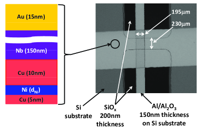
Our S/F/I/N tunnel junctions are fabricated by thermal evaporation and sputtering, using a series of mechanical masks (Fig. 1). We first evaporate a 150 nm strip of Al (N), then we immediately backfill the chamber with 300 Torr of a 10% O2, 90% Ar mixture. Exposing the freshly evaporated Al to the O2 quickly (while the Al is still hot) provides good conditions for oxide growth. The O2 exposure continues for 12 h to produce a robust layer of Al2O3 (I) on the Al surface. Next, we change masks and evaporate a thick layer (200 nm) of SiOx to define the junction geometry. When using mechanical masks for the top leads, shadow effects can cause unwanted regions at the edges of the junctions where the Ni thickness is not well defined. The SiOx is in place to avoid the appearance of edge effects in our data. Finally, we sputter a Cu(5nm)/Ni()/Cu(10nm)/Nb(150nm)/Au(15nm) multilayer. The choice of Ni and Cu is beneficial because our Ni has a relatively long spin-diffusion length, nm, as compared to our maximum Ni thickness, along with a low resistivity nm.Moreau:2007 Ni also provides weak asymmetry of spin-dependent scattering in the bulk and at Ni/Cu interfaces, and a low average Ni/Cu interface resistance.Moreau:2007 These attributes should simplify theoretical analysis. The Cu layer adjacent to the Al2O3 has been found to increase the effectiveness of the tunnel barrier. The Au deters oxidation of the Nb layer. Throughout the process we must break vacuum, but the consistency and reproducibility of our results suggest that this has little effect on the quality of our junctions. Due to a high level of oxygenation of our Al, its T K. Thus, we performed our measurements at 2.1 K, with the Al in the normal state.
Using a four-terminal lock-in technique, we measure the voltage-dependent differential conductance of our samples, , which approximates the DOS of our S/F bilayer. (The true DOS would be attained if measured at K when there is no zero-bias anomaly; we will use “DOS” to refer to our non-ideal differential conductance measurements.) We normalize by multiplying by the normal-state resistance , determined from the inverse of the differential conductance at large bias voltages. Our junction area-resistance products, m2, are substantially higher than those of other groups using passive oxidation,Otto:2007 ; Pothier:1997 but much lower than those produced by specialized oxidation techniques.Kontos:01 ; SanGiorgio:2008 From the data, it can be seen that this has little to no effect on our measurements.

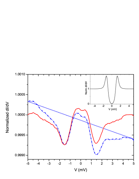
Our data exhibit a small negatively sloped, linear background, which appears to be a component of the normal state of our junctions. Figure 2 shows a plot of from our 4.5-nm sample before and after subtraction of the linear background, along with the linear fit to for , where mV is the gap parameter for Nb. There is another normal state characteristic which we do not correct for in our measurements. A slight V-shaped feature centered at 0 V becomes apparent at large Ni thicknesses. (It is visible on the red solid curve of Fig. 2 at mV.) We did not have a magnet on our apparatus to force the top Nb layer into the normal state; nevertheless, we emphasize that the slight negative slope and V-shaped feature in our background are both much smaller than background features observed in S/F/I/N tunnel junctions measured by other groups.KontosThesis ; SanGiorgioThesis
The inset of Fig. 2 shows a plot of for an N/I/S junction with a 15-nm Cu buffer layer between the Nb and Al2O3 layers. The standard N/I/S junction behavior illustrates the quality of the insulating barrier. The Cu buffer layer thickness in the N/I/S sample is the sum of the Cu layer thicknesses in the S/F/I/N samples. This was chosen to illustrate the minor effect of the Cu in the S/F/I/N samples as a whole. Even with this rather thick layer of Cu and the elevated temperature, we see a gap where nearly goes to zero. Another sign of junction quality is that is featureless for up to 10 mV (not shown), the maximum measured .

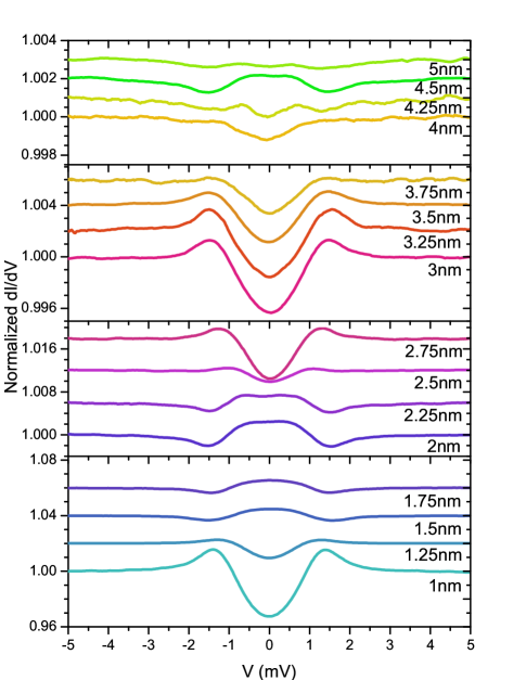
Figure 3 shows a plot of the DOS of our tunnel junctions while varying the Ni thickness. In a separate experiment at K, we measured the saturation magnetization of Ni()/Cu(5 nm) multilayers, for 1 nm5 nm. The data show an extrapolated non-magnetic “dead-layer” Ni thickness of nm at each Ni/Cu interface. Thus we show data only for nm. In the 1-nm sample one clearly sees the Nb gap, but with a significant suppression of the bulk Nb features due to the proximity effect in the strong ferromagnet. As we increase the Ni thickness, the zero-bias dip in the DOS quickly decreases in magnitude. At nm, we observe the first sign of an inversion in the differential conductance at zero bias, followed by a maximum inversion at nm. The features in at mV have also been inverted but occur at the Nb gap voltage in all the samples measured. The inversion cycles quickly and by nm, the samples return to the non-inverted regime. The dip in the DOS reaches its maximum at nm, then a second inversion occurs starting at nm. (The second inversion is more apparent in the expanded scale of Fig 2.) This second inverted state looks as though it might extend past 5 nm.

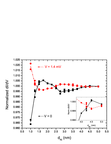
The oscillation is best illustrated in Fig 4 with a plot of the normalized differential conductance at both and mV versus Ni thickness. The oscillation period is irregular; the first inverted region persists for nm, while the second non-inverted region lasts much longer, for nm. One can see in the inset that the oscillation occurs about a value . This offset in the oscillation is due to the aforementioned, weak V-shaped zero-bias anomaly.
The transitions between normal and inverted DOS have been predicted to occur at F-layer thicknesses exactly half of where 0- transitions occur in S/F/S Josephson junctions.BuzdinReview After reviewing the literature on S/Ni/S junctions, we see that our junctions are most similar to those of Blum et al.Blum:02 and Shelukhin et al.,Shelukhin:06 where a Cu buffer layer is placed on each side of the Ni layer. In contrast, Robinson et al.Robinson:06 have Nb in direct contact with Ni, with a Ni “dead-layer” thickness of 0.8 nm at each Ni/Nb interface in comparison to our Ni dead-layer thickness of only nm at each Cu/Ni interface. The Ni thickness at which the first 0- transition is observed by these groups varies quite a bit – 2.6 nm, 1.7 nm (extrapolated value), and 3.8 nm, for Refs. [Blum:02, ], [Shelukhin:06, ], and [Robinson:06, ], respectively. Since our first 0- and -0 transitions occur at 1.3 and 2.5 nm, respectively, we would expect the first two transitions in S/Ni/S junctions to occur at 2.6 and 5 nm, in reasonable agreement with the values observed by Blum et al.Blum:02
Theoretical calculations of the DOS in S/F bilayers cover several regimes, defined by the relative strengths of the ferromagnetic exchange, , the superconducting gap parameter, , and the impurity scattering, , as well as the relative sizes of and the mean free path, . In the dirty limit, the Usadel equations provide a clearcut prediction of oscillation of the tunneling DOS, with period of order , where .Buzdin:2000 In the clean limit, the predictions are less straightforward. Solving the Eilenberger equation in the ballistic limit leads to the conclusion that the DOS does not oscillate in a semi-infinite ferromagnet.Buzdin:2001 ; Bergeret:2002 Oscillations are predicted to occur, however, in the presence of weak disorder, with an amplitude proportional to .Buzdin:2001 ; Bergeret:2002 With a finite ferromagnet, the oscillation is regained even in the pure ballistic limit due to specularHalterman:2002 or diffuseZareyan:2001 scattering from the film boundaries. In constrast, Sun et al. solved the Bogoliubov-deGennes equations and claimed that oscillations should occur in either a finite or semi-infinite F layer.Sun:2002
Because our observed DOS variations are not periodic in , we do not attempt to fit our data with Usadel theory. We believe that our samples most closely match the assumptions in the papers by Zareyan et al.Zareyan:2001 From earlier work on S/Ni systems, we expect that meV;Blum:02 ; Shelukhin:06 ; Robinson:06 and m/s for Ni,Petrovykh:98 while meV for Nb. From our measured Ni resistivity, nm, we deduce nm. This puts our samples in the “intermediate” regime with . By using Cu buffer layers next to the Ni, we limit the scattering events in our junctions considerably. As stated earlier, we find a spin diffusion length of 21 nm, low overall spin-scattering asymmetry, and very low Cu/Ni interface specific resistance in our multilayers: .Moreau:2007 This low interface resistance corresponds to a probability of scattering of only 15% at each Ni/Cu interface.ScatteringCalc The Cu/Nb interface is “rough” in the sense that there is significant diffusive scattering at this interface, as determined from its measured interface specific resistance of .Park:2000 This value of is larger than the total = 0.54 and 0.67 of the Cu/Ni/Cu region for = 1 and 5 nm, respectively. We also expect there to be diffuse scattering at the Cu/Al2O3 (tunneling) interface.
Plots of the energy dependence of the DOS shown in the papers by Zareyan et al.Zareyan:2001 agree qualitatively with our data. Performing a quantitative fit of the theory to our data, however, is problematic. The theory predicts that the first 0- transition should occur at very small , a flaw that may be correctable by adding spin-dependent interfacial phase shifts to the theory.Cottet:2005 (One could also argue that, because of the -nm dead layers at the two Cu/Ni interfaces, one should subtract 0.5 nm from our nominal sample thickness before fitting to the Zareyan theory, but that is not nearly enough to bring theory into agreement with experiment.) The theory also predicts large oscillations in the normalized DOS (i.e., large deviations from 1) at zero energy – much larger than what we observe in the experiment. The amplitude of the theoretical oscillations can be reduced by assuming a very small transparency of the Nb/Cu interface; such an assumption, however, is incompatible with the measured boundary resistance , which implies that .ScatteringCalc Strong spin-flip scattering would also reduce the amplitude of the DOS variations; the long measured spin memory length in our Ni films, however, precludes that explanation for these samples. One could assume that the variation in F-layer thickness over the junction area is very large, thereby smearing out the oscillations; we believe that such an assumption is unrealistic.
A previous measurement of the Nb/Ni systemSanGiorgio:2008 did detect signs of one transition, but the data contained additional low-energy features, which were later interpreted as signs of p-wave spin-triplet pairs.Lu:2010 We do not observe such low-energy features in our data.
In conclusion, we have observed multiple oscillations in the DOS of S/F bilayers as a function of F-layer thickness, where F is a strong ferromagnet (Ni). The oscillations can be described qualitatively, but not quantitatively, by the theory of Zareyan et al..Zareyan:2001 Discrepancies between theory and experiment may be due to the extra Cu layers in our samples, which are not present in the theoretical calculation, or to the absence of spin-dependent interfacial phase shifts in the theory.Cottet:2005
We acknowledge helpful conversations with M. Aprili and W. Belzig, technical assistance from R. Loloee and B. Bi, and use of the W.M. Keck Microfabrication Facility. This work was supported by the U.S. Department of Energy under Grant No. DE-FG02-06ER46341.
References
- (1) A.I. Buzdin, Rev. Mod. Phys. 77 935 (2005).
- (2) E.A. Demler, G.B. Arnold, and M.R. Beasley, Phys. Rev. B 55, 15174 (1997).
- (3) T. Kontos, M. Aprili, J. Lesueur, F. Genet, B. Stephanidis, and R. Boursier, Phys. Rev. Lett. 89, 137007 (2002).
- (4) V.A. Oboznov, V.V. Bol’ginov, A.K. Feofanov, V.V. Ryazanov, and A.I. Buzdin, Phys. Rev. Lett. 96, 197003 (2006).
- (5) T. Kontos, M. Aprili, J. Lesueur, and X. Grison, Phys. Rev. Lett. 86, 304 (2001).
- (6) V.V. Ryazanov, V.A. Oboznov, A.Yu. Rusanov, A.V. Veretennikov, A.A. Golubov and J. Aarts, Phys. Rev. Lett. 86, 2427 (2001).
- (7) Y. Blum, A. Tsukernik, M. Karpovski, and A. Palevski, Phys. Rev. Lett. 89, 187004 (2002).
- (8) H. Sellier, C. Baraduc, F. Lefloch, and R. Calemczuk, Phys. Rev. B 68, 054531 (2003).
- (9) V. Shelukhin, A. Tsukernik, M. Karpovski, Y. Blum, K.B. Efetov, A.F. Volkov, T. Champel, M. Eschrig, T. Lfwander, G. Schn, and A. Palevski, Phys. Rev. B 73, 174506 (2006).
- (10) M. Weides, M. Kemmler, E. Goldobin, D. Koelle, R. Kleiner, H. Kohlshedt, and A. Buzdin, Appl. Phys. Lett. 89, 122511 (2006).
- (11) J.W.A. Robinson, S. Piano, G. Burnell, C. Bell and M.G. Blamire, Phys. Rev. Lett. 97, 177003 (2006); Phys. Rev. B 76, 094522 (2007).
- (12) T.S. Khaire, W.P. Pratt Jr. and N.O. Birge, Phys. Rev. B 79 094523(2009).
- (13) S. Reymond, P. SanGiorgio, M.R. Beasley, J. Kim, T. Kim, and K. Char, Phys. Rev. B 73, 054505 (2006).
- (14) P. SanGiorgio, S. Reymond, M.R. Beasley, J.H. Kwon, and K. Char, Phys. Rev. Lett. 100, 237002 (2008).
- (15) C.E. Moreau, I.C. Moraru, N.O. Birge and W.P. Pratt, Jr., Appl. Phys. Letters 90, 012101 (2007).
- (16) E. Otto, M. Tarasov, and L. Kuzmin, J. Vac. Sci. Technol. B, 25, No. 4 (2007).
- (17) H. Pothier, S. Gueron, N.O. Birge, D. Esteve, and M.H. Devoret, Phys. Rev. Lett. 79, 3490 (1997).
- (18) T. Kontos, Ph.D. thesis, Université Paris XI, 2002.
- (19) P. SanGiorgio, Ph.D. thesis, Stanford University, 2008.
- (20) A. Buzdin, Phys. Rev. B 62, 11377 (2000).
- (21) I. Baladie, A. Buzdin, Phys. Rev. B 64, 224514 (2001).
- (22) F. S. Bergeret, A. F. Volkov, and K. B. Efetov, Phys. Rev. B 65, 134505 (2002).
- (23) K. Halterman and O.T. Valls, Phys. Rev. B 66, 224516 (2002).
- (24) M. Zareyan, W. Belzig, and Yu. V. Nazarov, Phys. Rev. Lett. 86, 308 (2001); Phys. Rev. B. 65, 184505 (2002).
- (25) G. Sun, D.Y. Xing, J. Dong, and M. Liu, Phys. Rev. B 65, 174508 (2002).
- (26) D.Y. Petrovykh, K.N. Altmann, H. Hochst, M. Laubscher, S. Maat, G.J. Mankey, and F.J. Himpsel, Appl. Phys. Lett. 73, 3459 (1998).
- (27) One can estimate the average transmission probability, , at an interface from the measured specific resistance, , using the Landauer approach. From Eqn. (6) in Schep et al.Schep:1997 one obtains the result . For Cu/Ni, this calculation gives , while for Nb/Cu it gives .
- (28) K.M. Schep, J.B.A.N. van Hoof, P.J. Kelly, G.E.W. Bauer, and J.E. Inglesfield, Phys. Rev. B 56, 10805 (1997).
- (29) W. Park, D.V. Baxter, S. Steenwyk, I. Moraru, W. P. Pratt, Jr., and J. Bass, Phys. Rev. B 62, 1178 (2000).
- (30) A. Cottet and W. Belzig, Phys. Rev. B 72, 180503(R) (2005); A. Cottet, ibid. 76, 224505 (2007).
- (31) W.J. Lu, Y.K. Bang, and K. Char, Phys. Rev. B 81, 144514 (2010).