Nanoscale magnetic field mapping with a single spin scanning probe magnetometer
Abstract
We demonstrate quantitative magnetic field mapping with nanoscale resolution, by applying a lock-in technique on the electron spin resonance frequency of a single nitrogen-vacancy defect placed at the apex of an atomic force microscope tip. In addition, we report an all-optical magnetic imaging technique which is sensitive to large off-axis magnetic fields, thus extending the operation range of diamond-based magnetometry. Both techniques are illustrated by using a magnetic hard disk as a test sample. Owing to the non-perturbing and quantitative nature of the magnetic probe, this work should open up numerous perspectives in nanomagnetism and spintronics.
The ability to map magnetic field distributions with high sensitivity and nanoscale resolution is of crucial importance for fundamental studies ranging from material science to biology, as well as for the development of new applications in spintronics and quantum technology Kirtley2010 ; Romalis_NatPhys2007 ; Bogani2008 . In that context, an ideal scanning probe magnetometer should provide quantitative magnetic field mapping at the nanoscale under ambient conditions. In addition, the magnetic sensor should not introduce a significant magnetic perturbation of the probed sample.
Over the last decades, different roads have been taken towards ultra-sensitive detection of magnetic fields including superconducting quantum interference devices (SQUIDs) Kirtley2010 , semiconductor-based Hall probes Kirtley2010 and optical magnetometers Romalis_NatPhys2007 . Even though extremely high sensitivity has been achieved with these devices, their spatial resolution remains limited at the micron-scale. Prominent approaches to reach nanoscale resolution are scanning-tunneling microscopy Heinze_Science2000 , mechanical detection of magnetic resonance Rugar_Nature2004 , nanoSQUIDs Yacoby_NanoLett2010 , X-ray microscopy Chao2009 and magnetic force microscopy (MFM) MFM . Since the latter technique operates under ambient conditions without any specific sample preparation, it is now routinely used for mapping magnetic field gradients around magnetic nanostructures. However, besides introducing an inevitable perturbation of the studied magnetic sample owing to the intrinsic magnetic nature of the probe Garcia2001 , MFM does not provide quantitative information about the magnetic field distribution.
Here we follow a recently proposed approach to magnetic sensing based on optically detected electron spin resonance (ESR) Chernobrod2005 . It was shown that this method applied to a single nitrogen-vacancy (NV) defect in diamond could provide an unprecedented combination of spatial resolution and magnetic sensitivity under ambient conditions Degen_2008 ; Taylor2008 ; Balasubramanian2008 ; Maze2008 . The principle of the measurement is similar to the one used in optical magnetometers based on the precession of spin-polarized atomic gases Romalis_NatPhys2007 . The applied magnetic field is evaluated by measuring the Zeeman shifts of the NV defect spin sublevels. In this article we demonstrate quantitative magnetic field mapping with nanoscale resolution, by applying a lock-in technique on the ESR frequency of a single NV defect placed at the apex of an atomic force microscope (AFM) tip. In addition, we report an all-optical magnetic imaging technique which is sensitive to large off-axis magnetic fields, and relies on magnetic-field-dependent photoluminescence (PL) of the NV defect sensor, induced by spin level mixing.
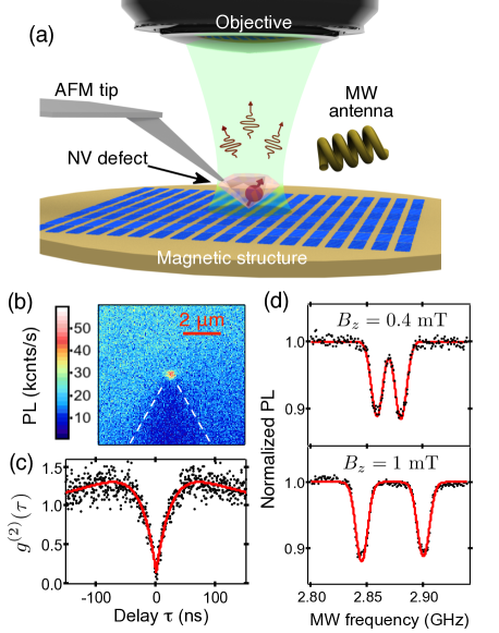
As depicted in Fig. 1(a), the scanning probe magnetometer combines an optical confocal microscope placed on top of a customized tuning-fork-based AFM (Attocube Systems), all operating under ambient conditions. The atomic-sized magnetic sensor was first engineered by grafting a diamond nanocrystal hosting a single NV defect at the end of the AFM tip Sup ; Cuche2009 ; Rondin2010 . After functionalization, a PL raster scan of the AFM tip shows an isolated spot at its apex (Fig. 1(b)), which corresponds to the collected light emitted by a single NV defect, as verified using photon correlation measurements (Fig. 1(c)).
The magnetic response of the probe was first characterized by sweeping the frequency of a driving microwave (MW) field through the spin resonance while recording the NV defect PL. Owing to spin dependent PL, ESR appears as a drop of the PL signal (Fig. 1(d)) Gruber_Science1997 . The spin Hamiltonian of the NV defect reads as Balasubramanian2008
| (1) |
where is the Planck constant, and are the zero-field splitting parameters, is the NV defect quantization axis, the electron gyromagnetic ratio, and the local magnetic field applied to the NV defect electron spin . For magnetic fields smaller than roughly 10 mT, i.e. such that , the quantization axis is fixed by the NV defect axis itself and the ESR frequencies are given by , where is the magnetic field amplitude along the NV axis. The spin orientation of the magnetic sensor was determined by recording ESR frequencies as a function of the orientation and the magnitude of a calibrated magnetic field Sup .
The shot-noise-limited sensitivity to d.c. magnetic field is linked to the minimum detectable magnetic field along the NV axis during an acquisition time through the relation Dreau2011
| (2) |
where is the rate of detected photons, the ESR contrast and the associated linewidth (FWHM). From the optically detected ESR spectra shown in Fig. 1(d), we infer T/. We note that this sensitivity could be significantly enhanced by using pulsed-ESR techniques Maze2008 ; Dreau2011 or by engineering a single NV defect in an ultra-pure diamond nanostructure MaletinskyArxiv_2011 .
The performances of the NV scanning probe magnetometer were characterized by mapping the magnetic field distribution created by a commercial magnetic hard disk. The magnetic bit geometry of this simple test sample is depicted in Fig. 2(a). As a first experiment, the magnetic sensor was approached at roughly nm from the sample surface. At such a distance, the random orientation of the magnetic bits provides non-trivial magnetic field patterns with a typical magnetic field magnitude in the mT range Sup . The simplest way to map such a magnetic field distribution is borrowed from magnetic resonance imaging Balasubramanian2008 . A MW field was applied with a fixed frequency corresponding to the zero-field ESR frequency. Iso-magnetic field images were then recorded by monitoring the NV defect PL while scanning the hard disk Balasubramanian2008 . Dark areas corresponding to zero magnetic field lines can be observed (Fig. 2(b)). However, the image exhibits a varying contrast related to inhomogeneous background luminescence from the sample. This limitation can be overcome by measuring the difference of PL for two fixed MW frequencies applied consecutively at each point of the scan (Fig. 2(c)). In this dual iso-magnetic field image, the contrast is significantly improved since background luminescence from the sample is suppressed.

Even with two iso-magnetic field lines recorded at once, the information remains incomplete. To determine the full magnetic field distribution, an ESR spectrum could be measured for each pixel of the scan. However, since a few seconds are required to record such a spectrum with a reasonable signal-to-noise ratio, this method would be extremely slow. To circumvent this limitation, a lock-in method was developed in order to track the shift of the ESR frequency while scanning the magnetic sample Schoenfeld2011 . This technique allows us to measure the strength of the magnetic field along the NV axis over the full scanning area with a typical sampling time of ms Sup . As shown in Fig. 2(d), the complete magnetic field map is in clear agreement with iso-magnetic field experiments. In addition, we note that the recorded pattern can be qualitatively reproduced by numerical simulations, both in shape, size, and magnetic field amplitude Sup . This confirms the reliability of NV-based scanning probe magnetometry for imaging non trivial magnetic field distributions at the nanoscale within a reasonable data acquisition time.
From the pixel-to-pixel noise in Fig. 2(d), an uncertainty T is deduced, which corresponds to a sensitivity T/, given the ms sampling time Sup . This value is in good agreement with the shot-noise-limited value calculated using Eq. (2). Regarding spatial resolution, the magnetic field is experienced by the NV defect electron spin wavefunction, resulting in a subnanometric probe volume. Experimentally the spatial resolution is rather limited by the pixel size (13 nm) and the positioning accuracy. The -map depicted in Fig. 2(d) is thus assumed to closely follow the actual field distribution – within the noise – with an overall spatial resolution of a few tens of nm. The line-cut in Fig. 2(d) further illustrates the ability to follow abrupt variations, up to 0.4 mT () between two adjacent pixels, corresponding to a field gradient of T/m. We emphasize the fact that no other instrument is able to quantitatively map magnetic field distributions with such a resolution.
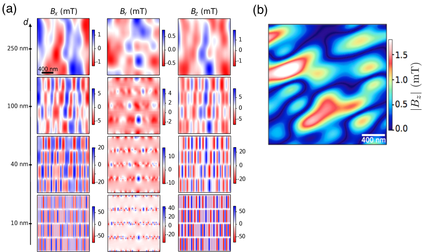
Yet, many material science studies are interested in the sample magnetization rather than the stray field . In this context, the spatial resolution is limited not only by the probe volume but also by its distance to the sample. Here for instance, simulations indicate that the magnetic bits could be resolved by using a probe-to-sample distance smaller than 40 nm (Fig. 3(a)) Sup . However, the magnetic field amplitude then reaches several tens of mT, including a component orthogonal to the NV defect axis Sup . In such a situation, the quantization axis becomes determined by the local magnetic field rather than the NV defect axis. The eigenstates of the spin Hamiltonian are therefore given by superpositions of the and spin sublevels, both in the ground and excited states Epstein2005 . As a result, optically-induced spin polarization and spin-dependent PL of the NV defect become inefficient, and the contrast of optically detected ESR vanishes. Magnetic field sensing using the previous techniques is thus not accessible in this high off-axis magnetic field regime ( mT). However, it was also shown that the NV defect PL drops by roughly when the magnitude of increases from to approximately mT Epstein2005 ; Lai2009 . This property can be exploited to perform a direct, microwave-free, magnetic field imaging using the single NV defect sensor.
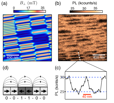
Figure 3(b) shows a PL image recorded while scanning the magnetic sample without applying any microwave field. In this experiment, an AFM feedback loop is applied to maintain the mean probe-to-sample distance to a constant value. Comparison with simulations (Fig. 3(a)) suggests that this distance is around 30 nm, limited by the diamond size and its position on the tip as well as by the tip oscillation. The PL image exhibits dark areas with a contrast greater than 20% which reveal the tracks and the bits of the magnetic hard disk. We note that the contrast depends on the field strength, which itself depends on the number of bits that are consecutively parallel. For instance, from the known bit-to-bit spacing of 55 nm, we deduce that the line-cut in Fig. 3(b) corresponds to a sequence , where and denote the two possible bit magnetizations (Fig. 3(b)-(c)). Each bit inversion gives rise to a stray field that appears dark on the PL image. We thus demonstrate a mode of NV-based magnetic field sensing that does not require the use of microwave and is sensitive to the off-axis magnetic field magnitude.
Summarizing, quantitative nanoscale magnetic field mapping with a sensitivity below T was demonstrated using NV-based scanning probe magnetometry. Moreover, we reported a microwave-free magnetic imaging technique that extends the range of application of NV-based magnetometry to large off-axis magnetic fields. Improvement of the sensitivity using pulsed-ESR techniques Dreau2011 , together with a better control of the NV-to-sample distance, should enable imaging of few-spins systems, which would be of great interest for fundamental studies in nanomagnetism and spintronics.
The authors acknowledge L. Mayer, O. Klein, F. Mazaleyrat, M. Lo Bue, P. Bertet, A. Slablab, T. Gacoin, F. Treussart, S. Huant, O. Mollet and O. Arcizet for fruitful discussions. This work was supported by the Agence Nationale de la Recherche (ANR) through the project Diamag, by C’Nano Île-de-France and by RTRA-Triangle de la Physique (contract 2008-057T).
References
- (1) J. R. Kirtley, Rep. Prog. Phys. 73, 126501 (2010).
- (2) D. Budker and M. Romalis, Nature Phys. 3, 227 (2007).
- (3) L. Bogani and W. Wernsdorfer, Nature Mater. 7, 179-186 (2008).
- (4) S. Heinze, M. Bode, A. Kubetzka, O. Pietzsch, X. Nie, S. Blügel, R. Wiesendanger, Science 288, 1805 (2000).
- (5) D. Rugar, R. Budakian, H. J. Mamin, and B. W. Chui, Nature 430, 329-332 (2004).
- (6) A. Finkler, Y. Segev, Y. Myasoedov, M. L. Rappaport, L. Ne’eman, D. Vasyukov, E. Zeldov, M. E. Huber, J. Martin and A. Yacoby§ Nano Lett. 10, 1046-1049 (2010).
- (7) W. Chao, J. Kim, S. Rekawa, P. Fischer, and E. H. Anderson, Opt. Exp. 17, 17669 (2009).
- (8) Y. Martin and H. K. Wickramasinghe, Appl. Phys. Lett. 50, 1455 (1987).
- (9) J. M. Garcia, A. Thiaville, J. Miltat, K. J. Kirk, J. N. Chapman, and F. Alouges, Appl. Phys. Lett. 79, 656 (2001).
- (10) B. M. Chernobrod and G. P. Berman, J. Appl. Phys. 97, 014903 (2005).
- (11) C. L. Degen, Appl. Phys. Lett. 92, 243111 (2008).
- (12) J. M. Taylor, P. Cappellaro, L. Childress, L. Jiang, D. Budker, P. R. Hemmer, A. Yacoby, R. Walsworth and M. D. Lukin, Nature Phys. 4, 810-816 (2008).
- (13) G. Balasubramanian, I. Y. Chan, R. Kolesov, M. Al-Hmoud, J. Tisler, C. Shin, C. Kim, A. Wojcik, P. R. Hemmer, A. Krueger, T. Hanke, A. Leitenstorfer, R. Bratschitsch, F. Jelezko and J. Wrachtrup, Nature 455, 648-651 (2008).
- (14) J. R. Maze, P. L. Stanwix, J. S. Hodges, S. Hong, J. M. Taylor, P. Cappellaro, L. Jiang, M. V. Gurudev Dutt, E. Togan, A. S. Zibrov, A. Yacoby, R. L. Walsworth and M. D. Lukin, Nature 455, 644-647 (2008).
- (15) See supplementary material at [URL will be inserted by AIP] for experimental details and numerical simulations of the magnetic field distribution above the magnetic hard disk.
- (16) A. Cuche, A. Drezet, Y. Sonnefraud, O. Faklaris, F. Treussart, J.-F. Roch, and S. Huant , Opt. Exp. 17, 19969 (2009).
- (17) L. Rondin, G. Dantelle, A. Slablab, F. Grosshans, F. Treussart, P. Bergonzo, S. Perruchas, T. Gacoin, M. Chaigneau, H.-C. Chang, V. Jacques and J.-F. Roch , Phys. Rev. B 82, 115449 (2010).
- (18) A. Grber, A. Drabenstedt, C. Tietz, L. Fleury, J. Wrachtrup, and C. von Borczyskowski, Science 276, 2012-2014 (1997).
- (19) A. Drau, M. Lesik, L. Rondin, P. Spinicelli, O. Arcizet, J.-F. Roch and V. Jacques, Phys. Rev. B, 84 195204 (2011)
- (20) P. Maletinsky, S. Hong, M.S. Grinolds, B. Hausmann, M.D.Lukin, R.-L. Walsworth, M. Loncar and A. Yacoby, Preprint arXiv:1108.4437.
- (21) R. S. Schoenfeld and W. Harneit, Phys. Rev. Lett. 106, 030802 (2011).
- (22) R. J. Epstein, F. M. Mendoza, Y. K. Kato, and D. D. Awschalom, Nature Phys. 1, 94-98 (2005).
- (23) N. D. Lai, D. Zheng, F. Jelezko, F. Treussart, and J.-F. Roch, Appl. Phys. Lett. 95, 133101 (2009).
I Supplementary methods
I.1 Experimental setup
The experimental setup combines an atomic force microscope (AFM) and a confocal optical microscope (AFM/CFM, Attocube System) as shown in Fig. 4). Two sets of piezoelectric actuators and scanners are used for positioning the sample and the AFM tip. The AFM cantilever is an Akiyama-Probe (Nanosensors) corresponding to a quartz tuning fork equipped with a micromachined silicon cantilever. The cantilever ends with a sharp tip whose nominal curvature radius is nm. A nanodiamond hosting a single nitrogen-vacancy (NV) defect is placed at the end of the tip as explained in the next section.
A continuous laser source operating at nm wavelength (Spectra-Physics Excelsior) is tightly focused at the end of the AFM tip through a microscope objective with a -numerical aperture and a -mm working distance (Olympus, MPLFLN100X). The photoluminescence (PL) emitted by a single NV defect placed at the apex of the tip is collected by the same objective and spectrally filtered from the remaining pump light using a dichroic beam splitter and a band-pass filter (Semrock, 697/75 BP) . Following standard confocal detection scheme, the collected light is then focused onto a -m diameter pinhole and directed to silicon avalanche photodiodes (Perkin-Elmer, SPCM-AQR-14) operating in the single-photon counting regime. Independently of the AFM scanners, precise positioning of the NV defect at the focus of the confocal microscope is achieved by scanning the laser beam with a fast steering mirror (Newport, FSM-300-02) combined with a pair of telecentric lenses. The focal length is adjusted by using the piezoelectric positioner of the AFM tip.
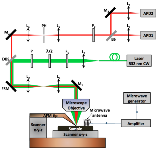
The unicity of the emitter was checked by using a Hanbury Brown and Twiss (HBT) interferometer consisting of two avalanche photodiodes placed on the output ports of a beamsplitter. The HBT detection system is associated with a fast multichannel analyser (Picoquant, TimeHarp 300) for recording the histogram of time delays between two consecutive single-photon detections. After normalization to a Poissonnian statistics, the recorded histogram is equivalent to a measurement of the second-order autocorrelation function Brouri . The observation of an anticorrelation effect at zero time delay, , is the signature that a single NV defect is addressed (see Fig. 1(c) of the main text).
For the electron spin resonance (ESR) measurements, a microwave synthesizer (Rohde & Schwarz, SMR20) is followed by a power amplifier (Mini-Circuits, ZHL-42) and connected to a -m-diameter copper wire directly spanned on the sample surface.
Scanning probe magnetometry is performed by monitoring the spin-dependent NV defect PL while scanning the magnetic sample. The tip-to-sample distance is adjusted using the piezoelectric scanner of the sample. For tapping mode operation, usual tuning-fork based AFM operation is used with a feedback loop adjusting the tip-to-sample distance.
I.2 Grafting a single NV defect at the end of the AFM tip
We started from commercially available diamond nanocrystals (SYP 0.05, Van Moppes SA, Geneva). Such nanocrystals are produced by milling type-Ib high-pressure high-temperature diamond crystals with a high nitrogen content ( ppm). The formation of NV defects was carried out using high energy ( MeV) electron irradiation followed by annealing at C under vacuum during two hours. The electron irradiation creates vacancies in the diamond matrix while the annealing procedure activates the migration of vacancies to intrinsic nitrogen impurities, leading to NV defect bonding. After annealing, the irradiated nanocrystals were oxidized in air at C during two hours. This procedure reduces the size of the nanodiamonds Gaebel and leads to an efficient charge state conversion of the created NV defects into the negatively-charged state Rondin2010 . After sonication and washing with distilled water, aqueous colloidal solutions of dispersed nanodiamonds, with a mean size of 20 nm, were obtained and finally deposited by spin-coating onto a silica coverslip.
A nanodiamond (ND) hosting a single NV defect was grafted at the apex of the AFM tip following the method introduced by Cuche et al. Cuche2009 ; Cuche2010 . The tip was first dipped in a solution of poly-L-lysine (EMS, molecular weight 30000-70000 u) for a few minutes. The tip as well as the sample of dispersed nanodiamonds were then mounted in the experimental set-up, and the NDs were optically characterized. Once a ND hosting a single negatively-charged NV defect was found, the sample was scanned with the AFM tip in tapping mode in a small area around the preselected ND. Electrostatic interactions between the polymer and the ND allow reproducible and robust grafting of the nanodiamond at the apex of the AFM tip.
I.3 Real-time tracking of the ESR frequency
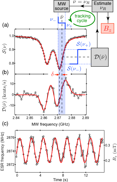
The lock-in method allowing to track the shift of the ESR frequency while scanning the magnetic sample is described in Fig. 5. Two slightly different microwave frequencies and , defined by , are applied consecutively and the PL difference is computed (Fig. 5(a) and (b)). This signal can be used as an error signal for tracking the ESR frequency Schoenfeld2011 . Indeed, if with smaller than the ESR linewidth (FWHM), the error signal is at first order proportional to the frequency detuning , i.e. to the magnetic field variation (Fig. 5(b)). Monitoring thus enables quantitative magnetic field mapping by continuously tracking the ESR frequency and measuring the frequency detuning from point to point, with a typical sampling time of ms. Reliability of this method is demonstrated by monitoring in real-time the magnetic field created by an AC current passing through a coil with a frequency up to Hz, as shown in Fig. 5(c).
I.4 Estimation of the magnetic field sensitivity
Since the magnetic stray field of the investigated hard disk is a priori not known, the measured field map (Fig. 2(c) in the main text) cannot be directly compared to theory. However, the field is assumed to vary slowly with respect to the spatial sampling, i.e. the pixel size, so that high-frequency components are attributed to measurement noise. Therefore, we introduce a pixel-to-pixel noise to estimate the experimental error . If is the matrix corresponding to the magnetic field map, with and , then can be defined as the standard deviation
| (3) |
which takes into account the pixel-to-pixel noise along both axis. For Fig. 2(c) of the main text, for which and , we find T. Given the acquisition time per pixel ms, an experimental field sensitivity T is obtained.
I.5 Determination of the NV defect axis
The NV defect axis, characterized by the unit vector , can be determined by measuring the ESR spectrum while applying a static magnetic field along several well-chosen directions. Denoting and the polar and azimuthal angles of the applied magnetic field in the reference frame of the NV defect, the diagonalization of the electron spin Hamiltonian (equation (1) of the main text) yields to the relation Balasubramanian2008
| (4) |
where and are the Zeeman-shifted ESR frequencies, while and are the zero-field splitting parameters of the NV ground-state electron spin. Since , one can use the approximation .
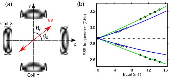
For a magnetic field applied along a given direction , Eq. (4) gives the angle between and . Repeating the measurement for two other directions of the magnetic field enables to completely determine . Since the magnetic images presented in the main manuscript are maps of the magnetic field component , it is important to know with respect to the reference frame of the laboratory. The orientation of the NV defect used in Fig. 2 and 3 of the main text was determined following the latter method. Fig. 6(b) shows the evolution of the measured resonance frequencies and as a function of a static magnetic field produced by two coils in an Helmholtz configuration. This field was first aligned along the -axis (filled circles) and then along the -axis (open circles). From these measurements and Eq. (4), the angles and were obtained. As , one deduces that lies in the plane. The actual orientation of the NV axis in the reference frame is illustrated in Fig. 6(a). The other orientation compatible with the set (,) was ruled out by a measurement along a third direction.
II Modelling of the magnetic field distribution above the hard disk
The magnetic sample used for the demonstration of magnetic field mapping is a piece of a commercial magnetic hard disk (Maxtor, 20 Gb). The geometry of the magnetic bits is depicted in Fig. 7. AFM topography of the sample allows to infer the geometrical orientation of the bits since grooves imprinted by the read/write head indicate the direction of the tracks (Fig. 7(a)). This information is used to determine the NV orientation with respect to the bits orientation.
The hard disk was modeled as an array of uniformly magnetized parallelepipeds (the ‘bits’). The dimensions of each ‘bit’ are nm, nm and nm, along , and , respectively, and their magnetization is depending whether the bit is at ‘0’ or ‘1’ (Fig. 7(b)-(c)). is the average magnetization of the ferromagnetic material. Typical value for the studied hard disk is T where is the permeability of free space. The pitch of the array is 55 nm along and 450 nm along .

The magnetic field distribution produced by a single bit (Fig. 7(c)) can be calculated using magnetostatics theory. Outside the parallelepiped, the three components of the magnetic field read as
| (5) |
| (6) |
| (7) |
The magnetic fields produced by each bit of the array were then summed up in order to compute the whole field distribution above the hard disk. Since the exact distribution of magnetic bit orientations is unknown, we compute the magnetic field distributions along , and directions for a random distribution of magnetic bits (Figure 8(a)). Figure 8(b) indicates the magnetic field distribution at nm from the hard disk, once projected along the axis of the NV defect used in the scanning-probe magnetometry experiments. The magnetic field follows rounded non trivial patterns with characteristics size and amplitude similar to the one observed experimentally (Fig. 2(c) of the main text). We note that the magnetic field distribution at another distance or along the axis follows a clearly different pattern.
References
- (1) R. Brouri, A. Beveratos, J.-P. Poizat, and P. Grangier, Opt. Lett. 25, 1294 (2000).
- (2) T. Gaebel, C. Bradac, J. Chen, P. Hemmer, and J. R. Rabeau, preprint arXiv:1104.5075 (2011).
- (3) L. Rondin et al., Phys. Rev. B 82, 115449 (2010).
- (4) A. Cuche et al., Opt. Exp. 17, 19969 (2009).
- (5) A. Cuche, A. Drezet, J.-F. Roch, F. Treussart, and S. Huant, J. Nanophoton. 4, 043506 (2010).
- (6) G. Balasubramanian et al., Nature 455, 648-651 (2008).
- (7) J. M. Garcia, A. Thiaville, J. Miltat, K. J. Kirk, J. N. Chapman, and F. Alouges, Appl. Phys. Lett. 79, 656 (2001).