μ
Material Science for Quantum Computing with Atom Chips
Abstract
In its most general form, the atom chip is a device in which neutral or charged particles are positioned in an isolating environment such as vacuum (or even a carbon solid state lattice) near the chip surface. The chip may then be used to interact in a highly controlled manner with the quantum state. I outline the importance of material science to quantum computing (QC) with atom chips, where the latter may be utilized for many, if not all, suggested implementations of QC. Material science is important both for enhancing the control coupling to the quantum system for preparation and manipulation as well as measurement, and for suppressing the uncontrolled coupling giving rise to low fidelity through static and dynamic effects such as potential corrugations and noise. As a case study, atom chips for neutral ground state atoms are analyzed and it is shown that nanofabricated wires will allow for more than gate operations when considering spin-flips and decoherence. The effects of fabrication imperfections and the Casimir-Polder force are also analyzed. In addition, alternative approaches to current-carrying wires are briefly described. Finally, an outlook of what materials and geometries may be required is presented, as well as an outline of directions for further study.
pacs:
37.10.Gh, 32.70.Cs, 05.40.-a, 67.85.-dWhatever the eventual physical realization is, quantum computing (QC) will most probably require fabrication technology, analogous but not identical to what has been done for classical computers. This is so also for the neutral particles described in this special issue.
Scalability will require highly repeatable architectures. Fidelity will require extremely low levels of DC fluctuations (e.g. electron or photon scattering due to imperfections such as surface roughness of wires and waveguides) and AC fluctuations in the form of electro-magnetic noise (the eventual numbers would be determined by the allowed infidelity or error rate, e.g. error1 ; error2 ). The variety of essential technologies for the different operations of a quantum computer such as isolation through vacuum, trapping, cooling, transporting, state preparation, manipulation, measurement and electronic readout, will require the accurate and complex integration capabilities which only monolithic fabrication methods exhibit. More so, it is plausible that the eventual realization will necessitate hybrid systems in which atoms serve, for example, as memory while superconducting circuits make up the logic gates. This integration between different quantum systems will most probably again require chip technology.
We may then talk of an atom chip for QC hosting any eventual desired particle and interaction, and where the atom chip may be very different from its form today RonRev ; ReichelRev ; fortagh . Indeed, already now diverse fabrication techniques are advancing at a rate which allows us to assume that any eventual scheme for the quantum computer may be put on an atom chip. This may include on one extreme cold atoms in an optical lattice within a miniature vacuum chamber inside a substrate, and on the other extreme, solid-state atoms or atom-like systems (e.g. NV centers in diamond nano crystals) embedded in a mesh of guides for photons and electrons fabricated on a surface. Our definition of the atom chip is therefore broadened to include all quantum objects close to a ”classical” surface. This somewhat arbitrary division does not include, for example, quantum dots and superconducting qubits which are an inherent part of the surface. The main focus of this paper will be on an atom chip having a room temperature surface.
When discussing a quantum system close to a macroscopic body one should think of a classical environment which is continuously attempting to lower the fidelity of the quantum operations by all means at its disposal. Hence, while the controlled coupling between this environment and our quantum system should be sufficient to enable necessary operations, we must suppress the uncontrolled coupling. The eventual figure of merit would then be the ratio between the controlled and the uncontrolled coupling, or more simply put, how many logic gate operations may be done with high fidelity. Due to the necessity of chip technology, as explained above, I believe that material science and technology will have just as much effect on this ratio as will the actual physical nature of the chosen quantum system and the experimental tools used to interact with it.
As the nature of the quantum system used changes, so does the nature of the coupling with the chip. For example, charged particles have exhibited a very strong dependence of the heating rate on the distance to the chip baruch ; dubessy ; ion_heating (most probably caused by contaminations or inhomogeneities on the surface chuang ). Polar molecules Meijer and Rydberg atoms Ryd_Spreeuw ; Ryd_Pfau ; Ryd_Scheel ; Ryd_Martin ; Ryd_Carsten , while exhibiting advantageous features concerning logic gates due to strong coupling, will also have enhanced atom-surface interaction relative to neutral atoms, as their permanent or induced dipole is much stronger.
In this paper we shall focus on ground state neutral atoms as a case study which should be followed for any system eventually used. The current-carrying wire will be used as a specific example of the problem of controlled vs. uncontrolled coupling. A brief discussion of an alternative atom chip in the form of an optical chip ends this paper.
I Advances in fabrication
Before discussing as a case study the fundamental limitations of the current-carrying wire, let us briefly note the state of the art in fabrication.
Since its conception, the vision of the atom chip has been to create a platform for any required atomic and molecular optics tool. In Fig. 1, a general view of such a vision is presented.

Advances in this direction have recently been made. For example, in the group of Dana Anderson, miniature vacuum chambers inside substrates are already functioning, and are poised to enable one of the best, if not the best, optical resolution to date; in the group of Ed Hinds an integrated pyramid magneto optical trap has been etched into the substrate; in the group of Robert Spreeuw, permanent magnet lattices have been fabricated; and in the group of Philipp Treutlein, multi-layer chips, including micro-wave guides, have been developed.
The vision for a quantum computer would be to create a dense lattice of traps which may be individually addressed and between which controlled coupling may be initiated. Such a lattice may have an optical periodicity if optical far fields are used, or sub-optical periodicity if near fields are used, or field sources such as current-carrying wires or permanent magnets, where the size limitation comes from e-beam lithography resolution, which today stands at a few tens of nano-meters. A procedure to optimize the chip design for such lattices has been defined roman . Another limitation comes from the smallest sustainable particle-surface distance (e.g. due to van der Waals forces) and this will be discussed to some extent in the following. Near every lattice site there will be another field source, such as a charged dot, or optical sub wavelength aperture (including plasmonics for enhanced transmission and focus), in order to facilitate single qubit rotations with single site addressability.
To facilitate rapid advances in the field of material science for atom chips, and with the aim of providing research and development services to the quantum optics community, we have constructed a fabrication facility at Ben-Gurion University with emphasis on quantum optics. This facility with a resolution of 10 nm and with the ability to integrate numerous materials and processes, has already given services to numerous laboratories in Europe and the United-States. Projects include current-carrying chips, permanent magnet chips, ion chips, chips for cold electrons, chips for diamond NV centers, photonics chips and so on. In Fig. 2, an ion chip developed for the Mainz group of Ferdinand Schmidt-Kaler is presented as an example.
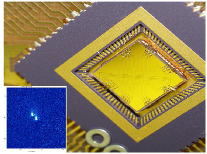
To conclude, these and other examples from the atom chip community chapter , as well as overwhelming advances in fabrication techniques in general, allow us the optimistic point of view that any eventual realization of a quantum computer may be put in the future on an atom chip. The main challenge will be to maximize the ratio of controlled to uncontrolled coupling, and in the following the current-carrying wire is analyzed as a case study.
II Atom-surface distance
For any system eventually used, it seems reasonable to assume that small system-environment distances will eventually be required. This is due to physical needs such as resolution and density of traps, as well as technical needs such as low power consumption.
In the neutral atom example, decreasing the atom-surface distance should increase trap gradients sufficiently to construct tunneling barriers with widths on the order of the atomic de Broglie wavelength. In the context of QC, this will allow for higher fidelity gates when they are potential dependent. The effect of small atom-surface distances will be quantified in the following section. High gradients also mean that qubits are better localized and this would be important for any 2-qubit interaction which is sensitive to the distance. Better localization is also important for single qubit rotation, as fixed elements contributing to such a rotation (e.g. charged dots) will be better spatially aligned with the qubit. Such high trap gradients may also allow for improved atom-light interactions such as probing without heating in the Lamb-Dicke regime, or side-band cooling.
At small atom-surface distances, interactions with the nearby surface become important. For example, spatial and temporal magnetic field fluctuations, due to electron scattering and Johnson noise, respectively, determine the minimal atom-surface distance, as they cause potential corrugations, spin-flips, and decoherence. There have been several experiments utilizing cold atoms to study these interactions tubingen_frag ; Hinds_spinflip ; orsay1 ; MagScanN ; simonSc ; emmert , and many suggestions on how to overcome their damaging effects Valery ; OrsayFragSup ; fermani ; YoniPRB ; TalAni ; peter . Also becoming prominent for small atom-surface distances is the Casimir-Polder (CP) force Milton ; being attractive, it reduces the magnetic barrier and allows atoms to tunnel to the surface, as already observed VuleticCP ; cornell . Several accurate measurements of the van der Waals, Casimir and CP forces between atoms and surfaces have been made hinds_vdw ; vigue . These topics will be elaborated upon in the following.
As atom-surface proximity grows so will the need for suppressing hindering surface effects by material science and engineering. The final accepted levels of material infidelity would be defined by the final allowed gate infidelity which in turn depends on error correction thresholds.
Finally, let us note that from the above it is evident that achieving small atom-surface distances would not only be advantageous for atom optics and QC, but would also contribute to the fundamental study of atom-surface and surface phenomena. However, the topic of the atom as a probe is beyond the scope of this chapter (see for example simonSc ; YoniPRB ; atom-probe ; carsten_probe ).
Let me also note that there are numerous ideas aimed at bringing atoms closer to a surface or a macroscopic object Ovchinnikov ; Schmiedmayer ; Shevchenko ; rosenblit1 ; Ricci ; Bender ; Gillen ; Chang2009 , all of which are, however, not based on the current-carrying wire, the latter being the focus of this chapter. Some additional ideas for small atom-surface distances will be noted in the photonics section.
II.1 Control of Atom-Atom distance
As mentioned earlier, small atom-surface distances may be advantageous to QC devices because of different reasons such as power consumption. However, as noted, one of the most important features of a small atom-surface distance are the high potential gradients made available RonRev . These will enable not only high density lattices for atoms - as required by the demand for scalability, and a high degree of alignment - as required for single qubit rotations, but also high fidelity in the control of barriers between atom trap sites, as required for example by the collision gate (see first chapter of this special issue).
As an example of the fidelity awarded by a small atom-surface distance, let us briefly examine the technical stability of a single barrier between two qubit sites. Tunneling may be used as a figure of merit for this stability. As noted previously, stable control of high gradients will most likely be relevant at some level to any QC scheme with isolated particles, and so let us examine in the following the stability of a barrier, not only with the collision gate in mind.
To quantify such tunneling, let us construct a simple potential which has no direct connection to QC. Consider a waveguide formed by a single atom chip wire (in the direction) and an external bias field; current through a second atom chip wire in the direction, namely in a right-angle “X” wire configuration ReichelIFM , is added to generate a simple potential barrier. The configuration used here is, incidentally, exactly opposite to the “dimple” configuration recently used for compressing atom chip traps Horikoshi ; Anderson-poster .
For a specific atom-surface distance , the magnetic potential in the direction, generated by the crossing wire, is given by:
| (1) |
where is the permeability constant, is the atomic magnetic dipole moment along the direction of the trap bottom (Ioffe-Pritchard) field , and is the current in the crossing wire. A 1D single-particle tunneling probability through the barrier can then be calculated in the WKB approximation as
| (2) |
where is the kinetic energy of the atom and . Assuming a kinetic energy of K for a atom (corresponding to a free-particle de Broglie wavelength of m) in the state, we may then easily calculate the change required in the current in order to cause a given proportional change in the tunneling probability, as a function of the atom-surface distance . The results of this calculation are shown in Fig. 3 for changing the tunneling probability from 0.001 to some higher probability. The calculation suggests that control over the tunneling probability requires a distance on the order of m for experimentally reasonable values of current control. In the simple model of Eq. (1), this corresponds to a barrier half-width of m, comparable to experiments that have observed interference between adjacent wells with the addition of non-static fields JoergIFM ; Ketterle_int . Thus, the desired static magnetic potentials can be generated only if atoms can be brought down to micron or sub-micron distances above the wires on the atom chip surface, at which point the tunneling rate can be tuned over a significant dynamic range by adjusting the current in the crossing wire, or in other words the high gradient potential is much more stable against current noise.
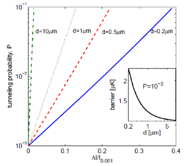
As another brief example of the enhanced trapping potential engineering resolution as the atom-surface distance is decreased, let us examine the creation of a 1D lattice by a ”snake”-shaped current-carrying wire.
Shaping the wire edges may be used for creating potential variations desired for manipulating atoms near the atom chip surface. In the following section we shall characterize the dependence of magnetic field variations on wire edge imperfections. Based on this dependence we may now discuss quantitatively the deliberate “tailoring” of magnetic trapping potentials by engineering wire edge profiles. Using again tunneling as a figure of merit for the purposes of this brief demonstration, we are particularly interested in potentials with sufficient variation so that tunneling barriers can be controlled. We may now wish to determine the highest “potential resolution”, namely, the smallest distinguishable distance between adjacent wells separated by static tunneling barriers, as a function of .
As a test case for quantifying this potential resolution, let us consider a configuration in which a thin wire is curved with a certain periodicity that corresponds to a wave-vector . If the amplitude of this curvature is small with respect to the wavelength, then, as will be explained in the next section, the magnetic field above the wire is given by a single component in Eq. (18), and then , where (see Appendix A for details).
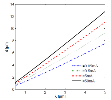
At the minima of such a periodic potential, the longitudinal frequency is , where is the atomic mass. In order to engineer potential barriers between adjacent minima higher than the single-atom ground state energy by a factor of say , we require , or . In Fig. 4 we plot the maximum atom-surface distance for which a longitudinal barrier with can be obtained. These curves show that the maximum atom-surface distance still allowing tunneling control is on the order of the potential periodicity . Designing the edges of a wire as the sum of different modulations therefore allows engineering of any periodic potential up to a resolution determined by the atom-surface distance. Consequently, atom-surface distances of m (or sub-micron distances in some cases) will be required to fully exploit the potential of an atom chip based on static magnetic fields.
Let us note that it stands to reason that a quantum information processing device based on ground state neutral atoms and current-carrying wires will also require static electric fields (e.g. for Stark shifts useful for single site addressability or barrier control), RF fields and MW fields (e.g. for controlling barriers, see for example MWgate ; Treulein_MW ). All these forms of radiation address the atom in the near field and so they may all be viewed as static fields. Hence the above discussion of a static barrier is relevant also to these fields. Namely, the closer the atom to the radiation source, the higher the gradients and the possibility to act locally and with greater immunity to instabilities.
As an example of quantitative considerations concerning gradients, let us utilize a square cross section wire. If is the atom-surface distance and we want to increase the lattice density by decreasing the trap-trap distance linearly with , to maintain the same trap depth the gradients will obviously need to grow as . However, to avoid finite size effects, the wire width should also go down linearly with . This means that that the cross section will go down as . Maintaining a constant current density, this also means that the current goes down as canceling the natural gradient growth which is proportional to . We thus see that in order to reap the benefits of a small atom-surface distance in terms of high density lattices, one requires growing current densities, and indeed it has been shown that smaller cross section wires enable higher current densities groth (see also Fig. 15c).
Finally, it is noted above that in order to avoid finite size effects which degrade the trap gradient, the wire width should be on the same scale as the atom-surface distance, i.e. for the above noted heights of m (see Fig. 3) one requires a micron-scale wire. As will be shown in the following, it is advantageous to utilize even smaller wire dimensions, namely nanowires. This will enable improving operational parameters at the above heights, or decreasing the atom-surface distance even further without hindering effects. If, in the future, vdW and CP polder are manipulated efficiently, atom-surface distances may become on the order of hundreds or even tens of nano-meters, and to exploit the full potential of this, state-of-the-art fabrication will have to be utilized.
III Potential corrugations
From the early days of atom chips and to this day, the current-carrying wire has been the ’work-horse’ of this apparatus. It is therefore fitting that we use it as a case study in order to present how conducting research into material science and material engineering in the context of any required coupling, may result in the suppression of unwanted effects.
Every field source has its inherent inhomogeneities, whether AC or DC, which are bound to cause infidelities. When considering a current-carrying wire as the trapping potential, let us first note the effect of static potential corrugations caused by inhomogeneous electron trajectories, i.e. fluctuating current directions lukin-frag ; hinds-frag . Such potential corrugations may warp the potential and cause infidelity in potential dependent qubit rotations and logic gates.
Such current irregularities are produced by wire imperfections, namely, geometrical properties (wire edge roughness and surface roughness), and internal bulk inhomogeneities. Since atom chip traps are formed by canceling the magnetic field generated by the current density at a specific distance from the wire , the minimum of the trapping potential lies along the wire direction . Variations in this potential are then directly related to changes in the direction of the magnetic field generated by the wire imperfections.
In previous work simonSc ; YoniPRB , we concluded that internal bulk inhomogeneities play a minor role in thin wires (thickness nm). For wide wires, surface roughness dominates the potential corrugation, but as we show, edge roughness dominates for narrow wires. Consequently, as we are interested in narrow wires in order to avoid finite size effects as discussed above, here we need to consider only current deviations due to edge roughness since the wires considered are thinner and narrower than nm. In Appendix A the theory for narrow wires is detailed. A general theory for all wire dimensions is presented in YoniPRB .
In Fig. 5, one may view the calculated directional variations of the magnetic field , generated by the trapping wire, as a function of the atom-surface distance for several wire cross-sections. The edge roughness amplitude is measured from our fabricated wires and was found to be frequency-independent [ in Eq. (20)] with a measured root-mean-square deviation of nm between nm [Let us note that in the case of edge roughness with power spectrum (), the directional variations of the magnetic field will be an order of magnitude higher ( compared to at m), and will lead to significantly larger density perturbations.]. In accordance with Eq. (20), we see that, for a given edge roughness (where is the position of the center of the wire), smaller wires produce only slightly larger magnetic corrugations. We also see that the influence of the surface roughness is negligible for the narrow wires discussed in this work due to the suppression of long wavelengths in the magnetic corrugations YoniPRB .
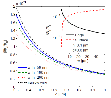
We thus find that as the atom-surface distance becomes closer, the corrugation amplitude increases. Furthermore, as the distance decreases shorter and shorter wavelengths affect the potential, and hence on the scale of a single qubit site or in the distance between two qubit sites, significant potential changes may arise.
III.1 Material engineering for potential corrugations
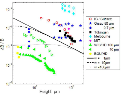
One way to solve the problem is through better fabrication of the standard gold wires. In Fig. 6, comparative data is presented showing that different methods may deliver very different corrugation magnitudes. The lift-off method used by BGU seems to be the best to date. However, more work is required to improve edge roughness.
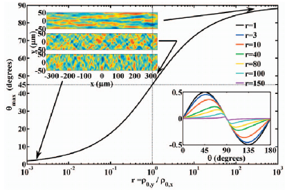
Another route to minimizing static corrugations is by different choices of wire material. An example of a class materials that may reduce electron scattering are electrically anisotropic materials YoniPRB . Here, low transverse conductance will suppress scattering into the transverse direction. One should remember that it is exactly this kind of scattering which causes potential corrugations. In Fig. 7 a calculation is presented showing that not only do these materials change the pattern of scattering, but they also suppress their amplitude considerably.
IV Johnson noise
Let us now continue with the analysis of our case study concerning the benefits awarded by material science and engineering. As current-carrying wires require metallic layers, let us analyze possible sources for AC fluctuations, i.e. noise. Such fluctuations can arise from technical noise in the wires or thermally activated electron currents, and may cause trap loss (spin-flip), climbing the vibrational level ladder (heating) and dephasing (decoherence).
The theory describing the affect of thermal noise Carsten_thermal ; Sidles on ultra cold atoms is now well established for isotropic materials (e.g. RonRev ; HenkelFundamentalLimits ; HenkelPotting ; HenkelPottingWilkens ; ScheelSpatialDecoherence ). Much of the existing theory was developed and explained by Carsten Henkel. Other models, based for example on non-local electrodynamics, have also been developed baruch .
The method typically used, incoherently adds up elementary current sources in the material, within the quasi-static approximation HenkelPotting . Although approximate (up to corrections on the order of a factor 2), this approach can be used to obtain closed-form solutions for many wire geometries. This is in contrast to methods based on Green functions, which are accurate but limited to simple geometries such as a half-space or a laterally infinite layer. It should be noted that the quasi-static approximation is valid when the skin depth (where , , and are the electrical conductivity, permeability of free space, and the radiation frequency, respectively) is much larger than both the atom-surface distance and the wire thickness . At room-temperature the skin depth of Au at MHz is on the order of m. The electrically anisotropic materials, which will be discussed in the following, usually have a much higher resistivity, and their skin depths are orders of magnitude larger at the same frequencies (e.g. for graphite mm). The quasi-static approximation thus applies even better to the latter. This approximation has been corroborated to a high degree of accuracy in experiment Valery ; VuleticCP and theory Zhang07 .
Let us briefly review the basic theory. The thermal radiation couples to the atoms’ magnetic moment by the Zeeman interaction , where is the magnetic dipole moment operator. This operator can be written for convenience as , with Bohr’s magneton, the Landé factor of the appropriate hyperfine level, and the total spin operator. As the magnetic field noise is random in time and space it averages to zero, and its effect is expressed through its two-point correlation function , between different points in time and space .
The field and magnetic moment being vectors, one actually needs the cross-correlations between their components to characterize the different processes induced by the noise (spin-flips, heating, and decoherence). It follows from time-dependent perturbation theory that the rate for a transition from an initial state to a final state of the system is given by LandauLifshitz
where the indices label the Cartesian components of the magnetic field. The argument of the magnetic field in Eq. (IV) is the atomic position. The matrix elements thus involve spatial (overlap) integrals over the spatial wave function and magnetic field (e.g. see Eq. (9) below). These integrals can be written in terms of the two-point correlation function of the magnetic field. The integral of this correlation function over the time difference is related to the cross-spectral density of the magnetic fluctuations at positions , and at the transition frequency HenkelFundamentalLimits ; Mandel . This is defined as
or equivalently by
| (5) |
In cases where the spatial degrees of freedom can be considered classically, in Eq. (IV) can be taken as the coordinate of the atoms, giving rise to a position-dependent transition rate between spin states. Instead of the wave function overlap integrals, the coordinates are then taken as . For calculating at the trap center one takes Note:TrapInhomogeneity .
The noise power spectrum is quite flat at all relevant frequencies which correspond for example to transitions between Zeeman magnetic sub-levels (radio-frequency), or the trap vibrational states (Hz to kHz range). Hence a low-frequency limit can be taken. If this spectrum is not flat in the relevant frequency range, the time dependence of loss and decoherence processes is more complicated and does not reduce to a simple rate HenkelFundamentalLimits .
Spin-flips are transitions from trapped () to untrapped () internal states. These states are eigenstates of the spin operator component parallel to the quantization axis, defined by the static trapping field at the bottom of the trap (we neglect the magnetic field direction deviations at the edges of the trap). Due to the form of the dipole moment operator , the Zeeman interaction can induce a spin-flip only when the direction of the magnetic field fluctuation is perpendicular to the quantization axis. Hence, in this case, we can rewrite (IV) as
| (6) |
where we sum over the perpendicular components only, and take the matrix elements of the dipole moment between the states and . The spin-flip rate can be measured from the lifetime of a magnetic micro-trap, and by varying the trap distance one can discriminate loss due to surface induced magnetic field fluctuations, against trap loss of different origin Hinds_spinflip ; VuleticCP ; Cornell2 ; TubingenNoise ; ZhangNoise .
Decoherence or dephasing of a quantum superposition state can occur without changing the occupation of the states involved in the superposition, affecting only the phase. We distinguish between spin decoherence and spatial decoherence. The former involves the change of the relative phase of two internal states ( and ) in a superposition at the same spatial location , while the latter involves the change of the relative phase of two spatially separated components of the atom cloud (positions and ), trapped in the same internal state. Here we shall consider only ‘classical dephasing’ in which the phase change arises from the fluctuations in the Zeeman shift. Such shifts occur, to lowest order, for magnetic field fluctuations parallel to the atom’s magnetic dipole moment. Hence for both types of decoherence processes we need only the parallel component of the same power spectrum appearing in the spin-flip case (Eq. (6)). The spin decoherence rate can thus be written as
| (7) |
with being the differential magnetic moment of the two trapped states, and the low-frequency limit parallel component of the noise spectrum, at the trap center . This decoherence rate can be measured from the reduced contrast of interference fringes in a series of Ramsey spectroscopy experiments, performed as a function of the atom-surface distance. In fact, long coherence times have already been measured close to the surface ReichelClock . This measurement puts an upper limit on the decoherence rate as other processes may mask the dephasing due to Johnson noise (e.g. inhomogeneous magnetic field) ReichelRephasing .
For the case of a spatially separated superposition state, the rate of decoherence of the relative phase of the atomic states between two points involves the correlation function of the difference in the magnetic fields , and can be written as
| (8) |
where we denote for convenience , and assume a correlation spectrum symmetric in , and flat in frequency. We again take only the field components parallel to the quantization axis, that shift the relative phase between the two parts of the wave function. In Eq. (8) is the magnetic moment matrix element of the single internal state. The low-frequency limit is valid here as the “scattering cross section” for transitions involved in the decoherence process is in practice independent of the frequency HenkelFundamentalLimits ; ScheelSpatialDecoherence .
This decoherence rate can be measured by studying the interference pattern contrast reduction in double-well experiments JoergIFM ; Reichel2010 , where the atom cloud is separated in two parts, which are then held at a fixed separation for a given time. The interference pattern is obtained by overlapping the cloud parts upon release from the trap. The interference contrast is directly related to the product of split time and decoherence rate; it can be measured as a function of the atom-surface distance by repeating the measurement at different heights. It is interesting to note that while quite a lot of theory has been done, spatial dephasing on atom chips has not to this day been measured. This is probably due to the fact that most cold atom experiments utilize a BEC, and in this system phase diffusion due to atom-atom interaction is very fast. This measurement is of great interest as the correlation lengths of the noise need to be examined carefully. This number may have a dominant effect on what the -qubit dephasing time would be Nqubit1 ; Nqubit2 ; Nqubit3 ; Nqubit4 .
Finally, heating of the trapped atoms (as a result of exciting external degrees of freedom while retaining the same internal state) can also be caused by the coupling to the thermal radiation. The transition rate of atoms initially in the ground vibrational state to higher states with energy splitting is of the form HenkelFundamentalLimits
| (9) |
where we find once more the spin operator matrix element in the direction parallel to the quantization axis, and now also the wave functions of the levels involved in the transition . The spatial integration here provides a probe of the spatial correlation of the magnetic field noise. In practice, it is enough to consider transitions from the ground state to either of the first two excited levels RonRev .
Thus, we see that the important term common to all rates is the spectral density of the magnetic field fluctuations or power spectrum . This quantity holds all of the relevant information about the magnetic field fluctuations leading to the harmful processes, while the other terms in each of the rates describe the coupling of the noise to the atoms through the magnetic dipole moment. Furthermore, we see that a measurement of either the spin or spatial decoherence rates, or of the heating rate, will give strong indications to any of the other two of these three processes, as they all depend on the noise power of the same field component.
One may summarize these results with an example, as presented in Fig. 8, showing the increasing spin-flip rate as a function of decreased atom-surface distance. A qualitatively similar behavior is found for heating and decoherence, as the noise amplitude increases with decreasing distance.
IV.1 Material engineering for Johnson noise
Typically, the noise spectrum is proportional to the ratio of the surface temperature and the surface resistivity HenkelFundamentalLimits . This seems to indicate that cooling the surface would not be advantageous as typically resistivity is linear with temperature. In fact, as is shown in Fig. 9, cooling of normal metals even worsens the situation. Although the eventual goal should be to utilize material science so as to realize an operational QC device at room temperature, cooling down to K should still be considered as technologically feasible. Let us therefore analyze the situation at low temperatures for standard conductors.
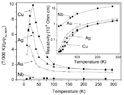
To avoid complications of magnetic permeability and hysteresis of the chip, let us consider here only nonmagnetic metals (having no long-range magnetic order). The resistivity of these metals is essentially a sum of two contributions : a temperature independent residual resistivity , due to scattering of charge carriers by crystal defects and impurities and a phonon contribution Valery . By manipulating the relative strength of these two terms we may engineer the ratio as a function of temperature. In Fig. 10 this ratio is presented as a function of the amount of defects introduced into the material.
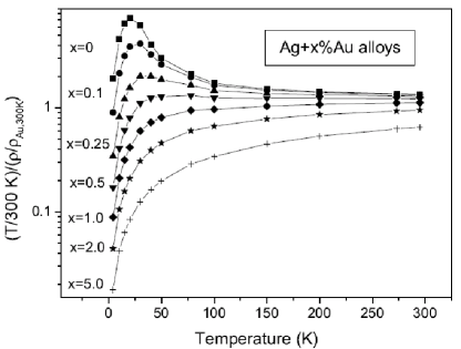
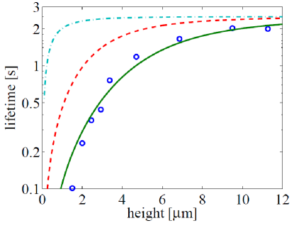
To conclude this first example of how material engineering may alter the hindering effect of Johnson noise, the expected lifetime as a function of atom-surface distance for different temperatures is presented in Fig. 11. To verify the theoretical calculation, a comparison to experimental results is also made. As can be seen, more than an order of magnitude improvement in lifetime may be achieved by simply introducing defects into the material.
As a second example for the potential advantages of material engineering for QC let us now calculate the possible suppression of the qubit dephasing by utilizing an anisotropic material instead of a normal metal. Although realistic hyperfine qubits will most likely use states between which only second-order Zeeman shifts and higher exist, for simplicity we shall use two qubit states differentiated by a first-order Zeeman shift.
As presented in the previous section, the noise power spectrum is related to the cross correlation function of the magnetic field fluctuations [Eqs. (IV),(5)]. Before calculating this correlation function, we define the coordinate system such that the wire length is along the direction, its width along the direction, and its thickness along . As in typical Ioffe-Pritchard magnetic traps, a non-zero field at the trap bottom polarizes the atoms along the wire, and so the quantization axis in our analysis is along the axis.
We can make a distinction between two types ofanisotropic materials. Materials with a ‘layered conductance’ are relatively good conductors along two axes and have one axis of bad conductance: . We always assume that the wire is aligned to one axis of good conductance, so that current may flow easily and create a magnetic trap. Materials that have only one direction of good conductance, or , will be denoted as ‘quasi-1D conductors’. A detailed treatment of the anisotropic material and the noise it induces, is presented in Appendix B.
In contrast to the case of spin-flips, the decoherence and heating rates, Eqs. (7,8,9), depend only on the noise in the parallel field component . This component may be strongly reduced for highly anisotropic materials. To quantify this, consider the ratio
| (10) |
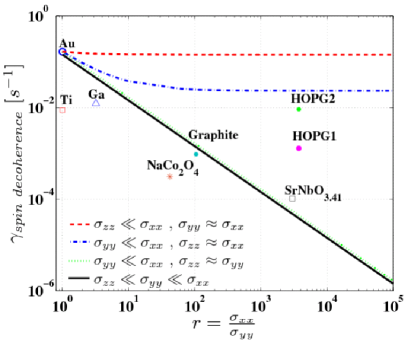
where are the conductivities and the geometry-dependent factors (see Appendix B), and where the reference level is an isotropic conductivity set to the ‘good axis’, . The possible improvements depend on the relative magnitudes of the anisotropic conductivities. Four cases can be distinguished, as illustrated in Fig. 12. For materials with layered conductance, the worst choice is to have the second good conducting axis in the chip plane, along the wire’s width: (dashed red line). The ratio (10) then tends to which is not significantly smaller than unity and where the conductivity anisotropy actually does not enter. With the other choice, having the badly conducting axis along the wire width (dashed-dotted blue), we get a reduction of about one order of magnitude for a small wire geometry. Materials that are quasi-1D conductive have a much larger potential for noise suppression: for comparable ‘bad axes’, , Eq. (10) scales inversely with the anisotropy ratio which may be very large. The suppression is somewhat more pronounced in the extreme case .
The reduction of the decoherence and heating rates is illustrated in Fig. 12 for the cases discussed above. We plot the spin decoherence rate (7) for a superposition state of the hyperfine levels and in the ground state of 87Rb. The anisotropic conductor is chosen such that the largest conductivity value coincides with the one for Au, an isotropic conductor taken as reference. The calculated rates for some specific materials are also given. It can be seen that quasi-1D materials are much more appealing to suppress heating and decoherence, although about one order of magnitude can already be gained with layered materials, even at a relatively small anisotropy. In addition, for most anisotropic materials, even the best direction conducts worse than Au; therefore the rates presented in this graph even for layered materials are smaller than for Au.
To conclude, heating and decoherence may be suppressed by several orders of magnitude even at room temperature, by using electrically anisotropic materials for current-carrying structures on atom chips.
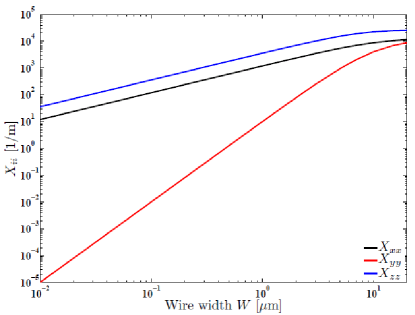
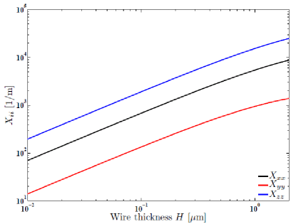
It is interesting to note that the anisotropic material hardly helps with the spin-flip rate as for the two perpendicular components and , which are responsible for spin-flips, we find that both mix the highly conducting and the low conductivity terms. The geometrical factors have been analyzed in detail (see appendix A in Valery ) for the case of rectangular wires. From this analysis it emerges that for any reasonable wire geometry, one cannot obtain the necessary situation in which the and factors are small relative to [see Eq. (30)]. This is presented in Fig. 13. Thus the main difference in the noise components is due to the difference in conductivity terms, where the conductivity is dominant. Consequently, the improvement to the trap lifetime using anisotropic materials at room temperature is expected to be at most on the order of .
Let us now briefly review some additional alternatives to normal metals:
Carbon Nano Tubes (CNTs) are an example of such a conductor. CNTs are able to hold a current density which is 2-3 orders of magnitude higher than that for gold. Consequently, although they have a very small cross section, they may hold enough current to create stable atom traps fermani ; CNT ; peano . As they are crystalline in nature, they may also reduce the static corrugation. Following from their small amount of material the CP force may also be suppressed, especially if the tubes are made to be suspended. In addition, contrary to normal metals, CNTs do not have a broad absorption spectrum and so they may be put close to optical high finesse elements without hindering their qualities. Let us note that CNTs may also be used for other purposes in the context of atom optics fortaghCNT ; Hau . See chapter for additional details.
Another material potentially advantageous for QC is the superconductor emmert ; roux ; valery2 ; mukai ; cano ; fortagh2010 ; fortagh2011 . These materials are expected to give rise to orders of magnitude less static scattering and noise. The drawbacks of superconductors include the cooling itself, the sensitivity to fabrication (e.g. the transition temperature is very sensitive to contaminations), DC fields and noise created by vortices, and current inhomogeneity (most of the current is in the wires edges). As trapping atoms in the field of vortices has been achieved ZhangSC ; muller , one may even contemplate the loading of a lattice of traps above a lattice of vortices. For more details of the state-of-the-art the reader is referred to Ref. chapter . As noted previously, the greatest challenge to material engineering is to enable long coherence times at room temperature, while maintaining a fast enough computer clock time.
Other metallic layers go beyond current-carrying structures and may include permanent magnets (which may also be made of non metallic or high resistivity materials) hinds_permanent ; amsterdam ; hannaford . Recent work amsterdam , also described in this issue, has realized a dense two dimensional array of trapped atoms and it seems reasonable to assume that controllable gates are feasible. The main advantages of permanent magnets are the lack of corrugations due to electron scattering and the suppressed Johnson noise due to the low conductivity of the material, as well as technical noise due to the lack of current. The main drawback is the demagnetization with temperature and time, and the weaker dynamic control of the fields.
Additional metallic structures not carrying current may include charged dots where the attractive potential is balanced by magnetic fields folman2003 , a magnetic mirror joerg1998 or evanescent waves Shevchenko2004 . As an example of such a lattice, an array of traps made of localized electric fields balanced by an evanescent field is presented in Fig. 14. While this example evokes fabricated electrodes, an advanced chip may utilize self assembled charged dots, where the limiting factor would be the charge diffusion rate.

Finally, we have not touched upon the issue of technical noise, namely, the current fluctuations in the current-carrying wire. The noise spectrum of the most fundamental noise limit, i.e. shot noise, increases as one over the distance square RonRev ; HenkelFundamentalLimits . This of course implies that going close to the surface may pose a serious problem, in which case techniques aimed at achieving sub-shot noise may have to be employed i.e. creating correlations between electrons (the mesoscopic community uses terminology such as ”distribution function of current”). However, long before this limit is reached, ”normal” technical noise, namely noise originating from the power supply or ”picked-up” by the cables that feed the atom chip ketterle_noise , will need to be suppressed. The effect of this noise may be very different from that of the Johnson noise discussed earlier. For example, contrary to the ”white noise” scenario utilized for Johnson noise, technical noise may be ”colored”. Such noise may, for example, cause asymmetric population transfers between the qubit states, if the potential is state dependent, as it is in the case of the collision gate shimi . In fact, if the center frequency or the shape of the noise are time dependent, this may cause population fluctuations, i.e. random walks on the -axis of the Bloch sphere (contrary to the equilibrium which is reached with white noise). To the best of our knowledge, only one measurement compared Johnson and technical noise on the same chip emmert .
V Nanofabricated wires
Let us finalize the discussion concerning current-carrying wires by analyzing the case of nanofabricated wires. Analyzing such wires is important when one wishes to answer the question of what is the smallest possible atom-surface distance. The answer to this question may reveal the fidelity limits induced by the current-carrying wire on the single qubit and 2-qubit operations. In this context, nanofabricated wires are important, for example, as noted previously, in order to avoid finite size effects which degrade the produced gradients. Smaller dimensions are also advantageous for reducing the amount of Johnson noise. In the following analysis we will also take into account the CP force.
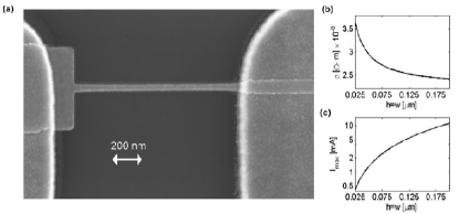
First, let us familiarize ourselves with how a nanofabricated wire looks like and behaves. A test wire fabricated at our facility and the calculated features of such a wire, are present in Fig. 15.
Next, let us take into consideration the CP force. The CP potential between a polarizable atom and dielectric or conducting objects casimir is one of the fundamental outcomes of zero-point vacuum fluctuations. It emerges from the fact that a dielectric or conducting object modifies the modes of the electromagnetic (EM) field in its vicinity, modes which interact with the atomic polarization. In our case, an attractive CP potential arises from the conducting gold nanowire and from the Si wafer coated with a nm thick SiO2 layer (used to prevent electrical shorts). The CP potential reduces the potential barrier for tunneling to the surface, thereby limiting the possibility of trapping atoms near the surface.
The EM modes of the combined surface+wire system are not analytically solvable and we will therefore carry out a separate examination of the CP potential emerging from the Si+SiO2 planar wafer, as discussed also in Ref. CNT , and from a simplified model that takes the wire as a perfectly conducting circular cylinder of a certain diameter. We then take the sum of the two contributions as an estimate for the combined potential as a sort of pairwise additive approximation (PAA). Based on earlier experience from the planar two-layer system, we may anticipate that this approach should at least give the right order of magnitude for the CP potential.
In general, the CP potential may be written in the form
| (11) |
where is the frequency-dependent atomic polarizability and is the trace over the Green’s tensor of the electromagnetic field at the same point , with being the Green’s tensor in empty space, responsible for a space-independent Lamb shift. For distances from the dielectric or conducting object much larger than , where is the wavelength corresponding to the lowest optical transition frequency, the CP potential generated by a planar structure made from a layer of thickness with a dielectric constant atop an infinitely thick dielectric layer of dielectric constant has the form (see Refs. Salem2010 ; CNT )
| (12) |
where is the static atomic polarizability. The dimensionless function takes the single-layer limiting value with when , and with when , where is on the order of unity. is obtained in the vicinity of a perfectly conducting thick layer. In our case is the ground state static polarizability of the atom, for the SiO2 layer, and for the Si wafer.
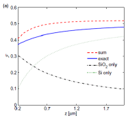
As stated above, we wish to compare contributions to the CP potential from the three different components comprising the surface: the Si chip, the SiO2 layer of thickness , and the gold nanowire of thickness . For this comparison to be meaningful, we require a common reference for the distance variable , which we define as the distance from the top of the SiO2 surface. Then the distance from the Si chip is nm and the distance from the top of the gold nanowire is . To factor out the strong dependence, we plot the quantity in Fig. 16(a) for the Si+SiO2 bilayer. This is compared to a sum of two models (shown separately in the figure): one where the half space for nm is full of Si while the other half is empty; and another in which only a nm thick SiO2 layer exists, with empty space for nm. The figure shows that simply summing the two potentials over-estimates the exact result by 8-15% over the relevant range, but it gives the right order of magnitude.
Next let us consider the CP potential for an atom at a distance from the center of a cylindrical conducting wire of radius where we set . It appears that the main contribution to the integral in Eq. (11) comes from frequencies on the order of . In our case, where m, the skin depth for a gold wire with resistivity is nm, which is much smaller than the width or thickness of the nanowires considered. We can therefore use a model where the wire is perfectly conducting (impenetrable for EM waves), such that the EM Green’s tensor is much simpler than in the general case. The CP potential is then given by
| (13) |
For the function is nearly linear, , tending to as , where the surface of the cylinder is similar to a planar conducting surface. In the opposite limit the function drops to zero as (see appendix in Salem2010 ).
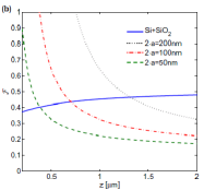
Figure 16(b) again shows the factor for the CP potential from the planar (i.e. Si+SiO2) surface in comparison to for cylindrical wires of different diameters . It is evident that the contribution of the wire is dominant when the distance from the wire is less than 5-7 times the diameter of the wire. For larger distances the contribution of the wire falls to half or less than the contribution of the surface. Given our experience with the bilayer system CNT , we expect the exact calculation of the wire+surface to deviate by the same order as we observe for the bilayer, namely, less than 20%. This degree of inaccuracy may also follow from the fact that the wires do not have circular cross-sections but square or rectangular ones. Therefore we believe that taking the sum of the two models can be expected to give at least an order of magnitude estimation of the CP potential.
Let us now calculate the tunneling to the surface. As a result of the CP potential, the magnetic barrier between the surface and the atoms is lowered, and atoms can tunnel through the barrier to the atomchip surface or wire. Calculated tunneling lifetimes are presented in Fig. 17, where we use a weighted average of the tunneling rate over all points in the plane. For each point we use the WKB approximation for tunneling through a one-dimensional potential barrier along the direction CNT :
| (14) |
where is the chemical potential in the case of ensembles or the energy in the case of single atoms, and the integration over is between the classical turning points and defined by . The weighted tunneling probability appearing in the integrand is given at any point by , where is the particle density and the transverse frequency is the inverse of the average round-trip time for a particle moving between the turning points []. In our example, these quantities are all calculated by solving the Gross-Pitaevskii equation for 1000 atoms of . In a typical trap generated by a Z-shaped wire, most of the tunneling occurs either at the center of the trap (where the atoms are closest to the wire) or at the trap ends (where the potential curves down towards the surface). Because of the much higher atom density directly above the wire, the lifetime is governed mostly by tunneling to the wire rather than to the surface.
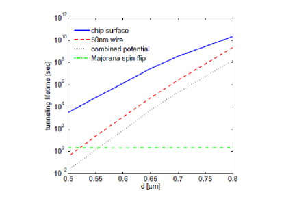
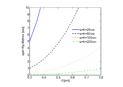
Next, let us also utilize the theory of Johnson noise as described previously, and present in Fig. 18 the spin-flip lifetime expected in a trap formed by a nano wire. One may clearly observe the much longer spin-flip lifetimes due to the smaller cross sections.
It is quite interesting to note that narrow wires are expected to give rise to much less decoherence, not only because of the small amount of material. It has been hypothesized that narrow wires suppress thermally induced transverse currents bruder . This is so because transverse currents charge the edges and the induced potential acts to suppress the currents. As surface induced decoherence is dominated by transverse Johnson noise currents, this may suppress decoherence by up to several orders of magnitude even at room temperature (in the same way as with anisotropic materials). For example, in Ref. bruder a decoherence rate of is calculated for a typical magnetic trap at m atom-surface distance while in Fig. 8 one finds for the spin-flip rate (which is very similar to the decoherence rate) .
Let us also briefly mention the issue of magnetic potential corrugations. One would expect that potential corrugations produced by edge roughness would grow considerably as the edges come in close proximity to the atom. However, as shown in Fig. 5, the rise is actually quite moderate (for square cross sections) as these fluctuations depend only on the variation of the center of the wire. Furthermore, the increase in potential corrugations due to edge roughness for narrower wires is somewhat balanced by the decrease of the other two sources: in Ref. YoniPRB and in Fig. 5 it has been shown that narrower wires will induce less surface (or bulk inhomogeneity) induced potential corrugations. This is so due to the discreteness of the resistance wave numbers when the random resistance fluctuations are analyzed as waves by Fourier transforming them. For a wire with a finite length and width , these wave numbers are integer products of and . As a consequence of this discreteness, the corrugations at long wavelengths are suppressed when the wire becomes narrower: the density of states becomes lower and no corresponding values of exist along the maximum scattering amplitude line of .
Finally, let us note the possible affect of anisotropic materials, mentioned previously, in the context of nanowires. Metallic nanowires have limited maximum current densities due to the increase in their wire resistivity (Fig. 15) from diffusive scattering at the wire surfaces. However, surface scattering for an anisotropic wire (where the surfaces are parallel to the good conductivity axis) may be significantly smaller and will have less effect on the wire resistivity, hence enabling higher current densities than discussed above. One may even speculate that at small dimensions the resistance relevant for the current density and that relevant for the Johnson noise may become decoupled.
Obviously it should be noted that nano-sized wires may have numerous limitations not presented here which need to be considered according to the specific implementation in mind. For example, introducing RF or MW currents into such wires may require more input power due to reduced impedance matching.
Let us summarize: We have discussed topics relevant to current-carrying wires including static and time dependent fluctuations and the CP force. Beyond the methods discussed above to suppress the hindering effects, one may speculate that additional methods may be found. As an outlook for future research, let us briefly give some examples of what these methods may be carsten_private .
-
•
CP force: There have been several experiments and theory papers showing that vdW and CP forces can be manipulated by choice of material and geometry, and may even change sign IntravaiaCP ; LeonhardtCP ; MundayCP ; YannopapasCP ; Pappakrishnan ; Sambale ; Milling ; Lee ; Tabor .
While it is completely unclear how this could be implemented in atom chips, the wealth of work done on this topic justifies an in depth look. Could, for example, the engineering of surface plasmons or of meta-materials achieve some kind of stealth coating that would cover a broad enough range of frequencies, so as to suppress reflection by absorbtion or perfect matching of the dielectric constants?
-
•
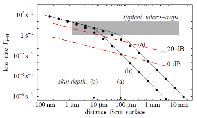
Johnson noise: The issue of Johnson noise seems to have several subtleties. Some of these may be viewed in Fig. 19.
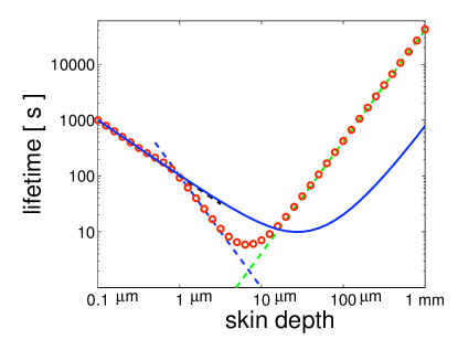
Figure 19: (Color Online) Lifetime vs. skin depth. The atom-surface distance is m. Solid line: bulk substrate (half space). Dashed lines and circles: 1m thick layer. The dashed lines show approximations (Table 2.2 in Bo ). The circles are computed numerically. Taken with permission from Bo . Similar results were obtained in scheel . More on layer vs. half space may be found in carsten_halfspace . At large skin depths the lifetime behaves as expected and goes up with skin depth simply because large skin depth mean small conductance and therefore a low level of noise. At medium skin depths, it is quite counterintuitive that a thin layer would enable smaller lifetimes than bulk. At small skin depths the situation is also not completely trivial. At very small skin depths, the lifetime of a thin layer behaves as a half space and goes up simply because no noise beyond a thin layer at the surface of the metal volume manages to reach the atom. The latter is hinting that if one manages to engineer a material that has a very small skin depth at the relevant frequencies for spin-flips, this could significantly suppress Johnson noise. If we cover our metal structures with such a ”cut-off” low-pass filter material for which the skin depth is larger than the ”filter” coating thickness for frequencies close to zero (so that DC magnetic fields or slow ramps could reach the atom), and for which the skin depth is much smaller than the ”filter” coating thickness for higher frequencies (starting from say MHz, the typical Zeeman splitting in atom traps), this would indeed manage to solve the problem of Johnson noise. It remains to be seen if meta-materials may be designed with these characteristics.
In addition, what is the origin of the ”kink” at a skin depth of m which is also the thickness of the wire? A plausible explanation is that some effect of the bottom surface of the metallic layer comes into play. This may hint at the fact that the bottom surface, or the interface between two materials at that surface, or some interference between the top and bottom surface of the metallic wire, has significant importance. Such effects have been discussed in 2surface1 ; 2surface2 ; 2surface3 . Let us note that Fig. 13 was made without including such a possible effect of the thickness. Understanding this effect may help think of ways to utilize it for a reduction of the noise.
To conclude the discussion on current-carrying wires, we may note that while conducting layers, wires and dots, offer significant potential for QC in their versatility, they also pose, as we have seen, significant challenges. It is therefore fitting to also briefly speculate upon a completely different type of atom chip which is all optical, i.e. completely made of dielectrics.
VI Photonics
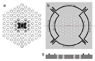
Although current-carrying elements are well poised to enable further advances (at room temperature or below), one may wish to look at alternatives even further than the charged electrodes or permanent magnets, both mentioned previously. One such alternative are all optical chips. Recent advances in Cavity-QED experiments rempe2011 clearly show that the control of light and atoms in the context of high quality optical elements is advancing quickly. The technological challenge of miniaturization and monolithic fabrication, as well as integration, is not to be underestimated, but seems to have no inherent limits (beyond the fact that a minimal number of atoms is required in order to define a smooth index of refraction). Indeed, photonics is an extremely fast advancing field which will most probably be incorporated in most scenarios as a tool supplementing the main technique of a future QC chip (an example of a combined photonic-electrical chip is presented in Fig. 20). As an in-depth analysis of the topic of photonics is beyond the scope of this paper, let us in the following briefly speculate on where this field may be headed.
Many advances have already been made. Outstanding experiments with fibers integrated on atom chips have been realized chapter ; reichel_cavity . Other experiments have trapped atoms very close to the surface of a fiber giving rise to the possibility of fiber lattices on chips fiber_lattice . However, it is hard to imagine that fibers will enable scalability. Let us therefore focus in the following on monolithic schemes.
Monolithic schemes may deal with near and far propagating fields as well as evanescent waves. Numerous impressive works are described in chapter and in this issue. Our own work folman_photonics deals mainly with micro disks and toroids as high-Q devices for a strong light-atom coupling. These devices may simultaneously trap, manipulate and measure atoms and so it may indeed be feasible to construct all optical atom chips. First experiments with these devices were done in 2006 by the groups of Vahala, Kimble and Mabuchi chapter . Other ideas for all optical chips have also been made (e.g. nakahara ). The first real integration of monolithic photonics with trapped atoms was made in the group of Ed Hinds hinds-photonics .
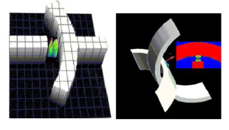
Material engineering may bring about the ability for completely novel geometries and functionalities. For example, as the ability to perform 3D fabrication advances, the presently planar chips, may enjoy 3D structures such as 3D stable mode light cavities (see Fig. 21). Another futuristic element would be curved blue detuned light mirrors enabling a stable cavity mode for matter-waves wilkens . Could this ”dark” trap turn out to be the least perturbing for the qubit?
Material engineering may also bring about a photonics revolution in atom chips via sub-wavelengths optics and plasmons. The control of plasmons and plasmon-emitted/absorbed/guided light by surface material and geometry engineering is quickly advancing plasmons . Here, very thin metallic layers or wires would control light beams with high accuracy and in small volumes. One may also think of utilizing voltage gates, as is done in directing and constricting the flow of 2D electron gases in mesoscopic physics, to dynamically control the shape of plasmons. Suggestions on how to use plasmons to trap atoms have already been made (albeit not on a flat surface) Chang2009 .
If dielectric atom chips are to be considered as a serious candidate for QC, one will of course have to return to the figure of merit discussed in the introduction, which is the ratio between the controlled and the uncontrolled coupling, or more simply put, how many logic gate operations may be done with high fidelity. Here a similar analysis to that presented above for ’electron carrying structures’, would have to be done to the ’photon carrying structures’. For example, in analogy to the hindering processes described above for a current-carrying wire one would need to analyze in detail the following issues:
-
•
Internal dynamic noise: In analogy to Johnson noise in current-carrying wires, changes in power, modes and polarization due to stress (e.g. due to vibrations) and temperature changes, or even frequency dependent index of refraction, are to be expected and should be analyzed. These fluctuations would create fluctuating level shifts in the qubit as well as possible excitations.
-
•
Internal corrugations: In analogy to magnetic potential corrugations due to static electron scattering in current-carrying wires, light scattering from surface roughness and bulk inhomogeneities will become a dominating factor. Light scattering does not only create intensity loss but changes light modes and may even reverse the light direction. For example, in folman_photonics we have analyzed the feasibility of maintaining small light scattering.
-
•
Technical noise: In analogy to technical noise in current-carrying wires, laser light intensity and frequency fluctuations will have to be taken into account.
Another issue is that of tunability. If high-Q devices are required, tunability will be necessary folman_photonics . If fast tunability is required, materials with a good Electro-Optical response need to be used. However, typically such materials have a crystalline form (e.g. ) and may not be deposited easily. More so, achieving very good surface roughness is challenging for these materials. New types of non-crystalline EO materials are being developed and should be studied in this context. Piezo materials may also be considered but again may suffer from the same problems. The state-of-the-art in tunability has been achieved in the group of Dan Stamper-Kurn and utilizes temperature control dsk .
Most, if not all, of the above tunability implementations require some electrical connection and this requires metal structures. Here one may again be forced to deal with some of the problems discussed above concerning current-carrying wires and an effort should be made to achieve an all optical chip (e.g. by changing the index of refraction with a pump beam).
Metallic surfaces may also be needed when reflecting surfaces are required, as high reflectivity dielectric mirrors are harder to make. Such a situation may arise when some high-Q devices such as Fabry-Pérot cavities are constructed (or even simply for a reflection Magneto-Optical Trap). As metallic surfaces give rise to Johnson noise, one should strive to find, by way of material engineering, high reflectivity - low conductance materials. Finding such materials is not trivial especially if one requires thin layers, in which case, these materials should be suitable for deposition by some evaporation or sputter method.
To conclude, the communication revolution of the last two decades and the development of the concept of a Lab-on-a-chip in the life science field, have brought about immense capabilities in the solid state miniaturization and integration of photonic elements. This gives rise to the hope that indeed monolithic dielectric devices for QC may be formed. However, just as in the case of the metallic layers, new figures of merits will have to be formed and much higher quality standards will have to be achieved.
VII Conclusion and outlook
The atom chip has come to life in the beginning of the 21st century and now, about a decade later, is the topic of intensive development in dozens of laboratories and fabrication facilities around the world. Analyzing the requirements of QC, such as accuracy, integration and scalability, it is likely that any implementation of a quantum computer will require chip technology and very advanced levels of material science and engineering.
As an example of the promise of material science and engineering, the case of current-carrying wires and ground state atoms was analyzed. Specifically, I have shown that for ground state atoms, nanofabricated wires enable the following advantages at room temperature and at an atom-surface distance below one micron:
-
•
coherence time of tens of seconds
-
•
spin-flip lifetime of tens of seconds
-
•
tunneling lifetime (to the surface) of tens of seconds
-
•
small static corrugation ()
-
•
strong immunity of magnetic lattice barriers against technical instabilities (above 10% change of current to change tunneling probability from 0.001 to 0.1).
The above means that considering Johnson noise and spin-flips, and for mili-second gate time scales MWgate ; JoergGate , ground state atoms may be able to award us with more than the threshold of gate operations. It is not the purpose of this paper to promote a specific scheme for QC but rather to emphasize by way of example, the promise of material science and engineering for any type of particle or interaction used.
Extrapolating from the advances made so far with atom chips, and taking into account the new micro and nano technologies being continuously developed, one may assume that any eventual implementation of QC will indeed be possible on future atom chips. While we wait for such an optimal implementation to be realized, the coupling between quantum information processing and material engineering, promises to bring about novel insights in both quantum optics and material science.
VIII Acknowledgement
I am sincerely thankful to Yonathan Japha and Carsten Henkel for many enlightening discussions and for their contributions over the years. I am also grateful to the members of the Ben-Gurion University atom chip group for their long standing efforts in this field. Finally, many thanks to the team of the fabrication facility for sharing my interest in building a bridge between material science and quantum optics, and for numerous chips they have so professionally fabricated for our lab and for labs around the world.
IX Appendix A: Magnetic corrugation above a narrow wire
Let us consider a fabricated metal wire carrying a total current . It extends along the direction and has a width along and thickness along . The boundaries of the wire are located at and . The corrugations of the wire boundaries and can be expanded as
| (15) |
A linear theory for small corrugations predicts that the effect of each spectral component of the corrugation is responsible for a corrugation of the magnetic field near the atomic trap center with a similar wavelength along the direction. However, the effect of components with wavelength much shorter than the distance between the wire and the atomic trap (on the order of hundreds of nanometers or more) drops exponentially as so that here we will only be interested in corrugations whose wavelengths are a few hundred nanometers or longer. We may then neglect the effect of spectral components on the order of the wire width or thickness and consider only corrugation terms with and , namely, we may assume that and depend only on .
Corrugations of the magnetic field along the main trapping axis above the center of a wire with geometrical perturbations are given by the Biot-Savart law as
| (16) |
where are the transverse current fluctuations in the wire. At the point exactly above the center of a nominally symmetric wire, it follows that only the symmetric components of [] and the anti-symmetric components of [] contribute to the magnetic field. The fabrication process typically provides wires whose edge corrugations are much larger than their top or bottom surface corrugations, so that the symmetric part of is the major contribution to the magnetic field fluctuations.
Ohmic theory, which is adequate when the width and thickness of the wire are much larger than the electron mean free path and whose use we justify below, predicts that for wavelengths longer than the wire width or thickness the symmetric -current fluctuations in the wire have the form
| (17) |
such that in the limit where , , where is the position of the actual center of the wire at a given point (). Substituting this limit into Eq. (16) while assuming small deviations of the wire edges from their nominal position, and assuming that , namely, the width of the wire is much smaller than the distance of the atom to the wire, we obtain the following expression for the magnetic field corrugations above the wire
| (18) |
where is the total current in the wire and is the modified Bessel function, which may be approximated by . Our model for the fluctuation spectrum assumes that , where is the edge fluctuation at some wavevector and then can be obtained by summing this spectrum over all . Typically, is a number between 0 (“white-noise spectrum”) and 1 (“1/f spectrum”), while is a random phase. It follows that the root-mean-square value of the field fluctuations is given by
| (19) |
If we assume that the distance is much shorter than the length of the measured wire, we obtain
| (20) |
where is the unperturbed magnetic field of a wire in the direction. Here has units of (length)1/2-α and is given by
| (21) |
where the sum is over values taking integer multiples of up to a cutoff . Typical values of this sum for and are and respectively, when .
The same result should be obtained if we consider diffusive surface scattering. As presented in Ref. Salem2010 , in nano-sized wires the conductivity near the boundary is reduced by diffusive surface scattering (with a typical exponential decay length from the wire edge, on the scale of the mean free path). This means that diffusive scattering is limited to a region of dimension smaller than . At the same time, the corrugation wavelengths relevant at the atom position, e.g. similar to or larger than the atom-surface distance, induce current density directional deviations away from the edge with an exponential decay length of . As most of the current will follow the corrugations of the boundary even in the case of surface diffusive scattering, such that the resulting -current fluctuations will again generate transverse components of the current proportional to the derivative . We thus use the ohmic theory whose general form was developed in Ref. YoniPRB to calculate the magnetic field corrugations above the wire.
X Appendix B: Johnson noise above an anisotropic material
Turning now to magnetic field fluctuations, we use the expression for the current cross correlation function Rytov ; LifshitzRef ,
| (22) | |||||
where is the Bose-Einstein occupation number, and where the dielectric tensor
| (23) |
is proportional to the conductivity tensor for homogeneous media. When the anisotropic crystal axes are aligned with the wire, the latter is diagonal,
| (24) |
This property will be used below. We assume here that the current in the material responds locally to the electric field (Ohm’s law), . The vector potential and its correlation function in the quasi-static approximation are given by
| (25) | |||
| (26) |
Here denote the two spatial locations for which we take the correlation function, whereas is the integration variable, such that we sum the contribution from all points within the material volume , which are at distances () from the locations . Note that this formula neglects jumps in due to surface currents at the metal-vacuum interface. In order to calculate the correlation function of the magnetic field fluctuations, we take the curl of the vector potential correlation function, once with respect to and once with respect to . Writing this in tensor form we get,
| (27) | |||||
using the Levi-Civita symbol and summing over repeated indices. We defined the integral holding the conductivity tensor and the geometry terms as for convenience, and the symbol () means a derivative with respect to in the direction of its th-component. Performing the derivatives we obtain
| (28) |
where the geometry of the system enters through the quantity :
| (29) |
We assume here a homogeneous medium (i.e., the components are spatially constant within the material volume ).
Again limiting the discussion to the ’aligned’ case (24), Eq. (28) is simplified, and in fact for every pair of we need to sum only two integrals. Considering the wire geometry to be such that the atoms are located above the center of a very long wire (), the only non-zero elements are () due to symmetry. Hence we obtain
| (30) | |||
and it is convenient to define
| (31) |
assuming the good conductivity to be along .
We see that in contrast to the isotropic case, where one has a single conductivity for all field components , here the conductivities give different weights to the geometry-dependent factors .
We can now write the full expression for the power spectrum, using (5) and collecting all of the prefactors omitted in (26),(27) as
| (32) |
where, following HenkelPotting , we have normalized the power spectrum to Planck’s blackbody formula
| (33) |
As the relevant frequencies are low, the high temperature limit of the Planck function is applicable, and thus the expression for the power spectrum approaches
| (34) |
This expression has the same form as the result for the isotropic case HenkelPotting , however here the tensor holds the anisotropic terms in it.
References
- (1) A. M. Steane, Overhead and noise threshold of fault-tolerant quantum error correction, Phys. Rev. A 68, 042322 (2003).
- (2) E. Knill, Scalable quantum computing in the presence of large detected-error rates, Phys. Rev. A 71, 042322 (2005).
- (3) R. Folman, P. Krüger, J. Schmiedmayer, J. Denschlag and C. Henkel, Controlling cold atoms using nanofabricated surfaces: Atom Chips, Adv. At. Mol. Opt. Phys. 48, 263 (2002).
- (4) J. Reichel, Microchip traps and Bose Einstein condensation, Appl. Phys. B 75, 469 (2002).
- (5) J. Fortágh and C. Zimmermann, Magnetic microtraps for ultracold atoms, Rev. Mod. Phys. 79, 235 (2007).
- (6) C. Henkel and B. Horovitz, Noise from metallic surfaces: Effects of charge diffusion, Phys. Rev. A 78, 042902 (2008).
- (7) R. Dubessy, T. Coudreau, L. Guidoni, Electric field noise above surfaces: A model for heating-rate scaling law in ion traps, Phys. Rev. A 80, 031402(R) (2009).
- (8) N. Daniilidis, S. Narayanan, S. A. Möller, R. Clark, T. E. Lee, P. J. Leek, A. Wallraff, St. Schulz, F. Schmidt-Kaler, H. Häffner, Fabrication and heating rate study of microscopic surface electrode ion traps, New J. Phys. 13, 013032 (2011).
- (9) S. A. Meek, H. Conrad, and G. Meijer, Trapping Molecules on a Chip, Science 324, 1699 (2009).
- (10) A. Tauschinsky, R. M. T. Thijssen, S. Whitlock, H. B. van Linden van den Heuvell, and R. J. C. Spreeuw, Spatially resolved excitation of Rydberg atoms and surface effects on an atom chip, Phys. Rev. A 81, 063411 (2010).
- (11) H. Kübler, J. P. Shaffer, T. Baluktsian, R. Löw, and T. Pfau, Coherent Excitation of Rydberg Atoms in Thermal Vapor Microcells, Nature Photonics 4, 112 (2010).
- (12) J. A. Crosse, S. A. Ellingsen, K. Clements, S. Y. Buhmann, and S. Scheel, Thermal Casimir-Polder shifts in Rydberg atoms near metallic surfaces, Phys. Rev. A 82, 010901 (2010).
- (13) J. D. Carter and J. D. D. Martin, Energy shifts of Rydberg atoms due to patch fields near metal surfaces, Phys. Rev. A 83 (2011) 032902.
- (14) M. M. Müller, H. R. Haakh, T. Calarco, C. P. Koch, and C. Henkel, Prospects for fast Rydberg gates on an atom chip, paper in this issue, arXiv:1104.2739 (2011).
- (15) S. X. Wang, Y. Ge, J. Labaziewicz, E. Dauler, K. Berggren, Isaac L. Chuang, Superconducting microfabricated ion traps, Appl. Phys. Lett. 97, 244102 (2010).
- (16) R. Folman, P. Treutlein, J. Schmiedmayer, Fabrication of Atom Chips, in ”Atom Chips” (Book by Wiley-VCH), Eds. Vladan Vuletic and Jakob Reichel.
- (17) R. Schmied, D. Leibfried, R. J. C. Spreeuw, S. Whitlock, Optimized magnetic lattices for ultracold atomic ensembles, New J. of Phys. 12, (2010).
- (18) J. Fortágh, H. Ott, S. Kraft, A. Günther, C. Zimmermann, Surface effects in magnetic microtraps, Phys. Rev. A 66, 041604 (2002).
- (19) M. P. A. Jones, C. J. Vale, D. Sahagun, B. V. Hall, E. A. Hinds, Spin Coupling between Cold Atoms and the Thermal Fluctuations of a Metal Surface, Phys. Rev. Lett. 91, 080401 (2003).
- (20) J. Estève, C. Aussibal, T. Schumm, C. Fig, D. Maill, I. Bouchoul, C. I. Westbrook, A. Aspect, Role of wire imperfections in micromagnetic traps for atoms, Phys. Rev. A 70, 043629 (2004).
- (21) S. Wildermuth, S. Hofferberth, I. Lesanovsky, E. Haller, L. M. Andersson, S. Groth, I. Bar-Joseph, P. Krüger, J. Schmiedmayer, Bose-Einstein condensates: Microscopic magnetic-field imaging, Nature 435, 440 (2005).
- (22) S. Aigner, L. Della Pietra, Y. Japha, O. Entin-Wohlman, T. David, R. Salem, R. Folman, J. Schmiedmayer, Long-Range Order in Electronic Transport Through Disordered Metal Films, Science 319, 1226 (2008).
- (23) A. Emmert, A. Lupaşcu, G. Nogues, M. Brune, J.-M. Raimond, S. Haroche, Measurement of the trapping lifetime close to a cold metallic surface on a cryogenic atom-chip, Eur. Phys. J. D 51, 173 (2009).
- (24) V. Dikovsky, Y. Japha, C. Henkel, R. Folman, Reduction of Magnetic Noise in Atom Chips by Material Optimization, Eur. Phys. J. D 35, 87 (2005).
- (25) J.-B. Trebbia, C. L. Garrido Alzar, R. Cornelussen, C. I. Westbrook, I. Bouchoule, Roughness Suppression via Rapid Current Modulation on an Atom Chip, Phys. Rev. Lett. 98, 263201 (2007).
- (26) R. Fermani, S. Scheel, P. L. Knight, Trapping cold atoms near carbon nanotubes: Thermal spin flips and Casimir-Polder potential, Phys. Rev. A 75, 062905 (2007).
- (27) Y. Japha, O. Entin-Wohlman, T. David, R. Salem, S. Aigner, J. Schmiedmayer, R. Folman, Model for Organized Current Patterns in Disordered Conductors, Phys. Rev. B 77, 201407(R) (2008).
- (28) T. David, Y. Japha, V. Dikovsky, R. Salem, C. Henkel, R. Folman, Magnetic interactions of cold atoms with anisotropic conductors, Eur. Phys. J. D 48, 321 (2008).
- (29) G. Sinuco-León, B. Kaczmarek, P. Krüger, and T. M. Fromhold, Atom chips with two-dimensional electron gases: Theory of near-surface trapping and ultracold-atom microscopy of quantum electronic systems, Phys. Rev. A 83, 021401(R) (2011).
- (30) K. A. Milton, Resource Letter VWCPF-1: Van der Waals and Casimir-Polder forces, arXiv:1101.2238v2 (2011).
- (31) Y. J. Lin, I. Teper, C. Chin, V. Vuletić, Impact of the Casimir-Polder Potential and Johnson Noise on Bose-Einstein Condensate Stability Near Surfaces, Phys. Rev. Lett. 92, 050404 (2004).
- (32) J. M. Obrecht and R. J. Wild and M. Antezza and L. P. Pitaevskii and S. Stringari and E. A. Cornell, Measurement of the Temperature Dependence of the Casimir-Polder Force, Phys. Rev. Lett. 98, 063201 (2007).
- (33) V. Sandoghdar, C. I. Sukenik, E. A. Hinds, Direct measurement of the van der Waals interaction between an atom and its images in a micron-sized cavity, Phys. Rev. Lett. 68, 3432 (1992); C. I. Sukenik, M. G. Boshier, D. Cho, V. Sandoghdar, E. A. Hinds, Measurement of the Casimir-Polder force, Phys. Rev. Lett. 70, 560 (1993).
- (34) S. Lepoutre, V. P. A. Lonij, H. Jelassi, G. Trénec, M. Büchner, A. D. Cronin and J. Vigué, Atom interferometry measurement of the atom-surface van der Waals interaction, Eur. Phys. J. D (2011).
- (35) M. Gierling, P. Schneeweiss, G. Visanescu, P. Federsel, M. Häffner, D. P. Kern, T. E. Judd, A. Günther, and J. Fortágh, Cold-atom scanning probe microscopy, Nature Nanotechnology 6, 446 (2011).
- (36) H. R. Haakh and C. Henkel, Magnetic near fields as a probe of charge transport in spatially dispersive conductors, arXiv:1107.2268v1 (2011).
- (37) Yu. B. Ovchinnikov, S. V. Shulga, V. I. Balykin, An atomic trap based on evanescent light waves, J. Phys. B 24, 3173 (1991).
- (38) J. Schmiedmayer, Quantum wires and quantum dots for neutral atoms, Eur. Phys. J. D 4, 57 (1998).
- (39) A. Shevchenko, T. Lindvall, I. Tittonen and M. Kaivola, Microscopic electro-optical atom trap on an evanescent-wave mirror, Eur. Phys. J. D 28, 273 (2004).
- (40) M. Rosenblit and Y. Japha and P. Horak, R. Folman, Simultaneous optical trapping and detection of atoms by microdisk resonators, Phys. Rev. A 73, 063805 (2006).
- (41) L. Ricci and D. Bassi, A. Bertoldi, Combined static potentials for confinement of neutral species, Phys. Rev. A 76, 023428 (2007).
- (42) H. Bender, P. Courteille, C. Zimmermann, S. Slama, Towards surface quantum optics with Bose-Einstein condensates in evanescent waves, Appl. Phys. B 96, 275 (2009).
- (43) J. I. Gillen, W. S. Bakr, A. Peng, P. Unterwaditzer, S. Fölling, M. Greiner, Two-dimensional quantum gas in a hybrid surface trap, Phys. Rev. A 80, 021602(R) (2009).
- (44) D. E. Chang, J. D. Thompson, H. Park, V. Vuletić, A. S. Zibrov, P. Zoller, and M. D. Lukin, Trapping and Manipulation of Isolated Atoms Using Nanoscale Plasmonic Structures, Phys. Rev. Lett. 103, 123004 (2009).
- (45) W. Hänsel, J. Reichel, P. Hommelhoff, T. W. Hänsch, Trapped-atom interferometer in a magnetic microtrap, Phys. Rev. A 64, 063607 (2001).
- (46) M. Horikoshi and K. Nakagawa, Atom chip based fast production of Bose-Einstein condensate, Appl. Phys. B 82, 363 (2006).
- (47) D. Z. Anderson, private communication (2009).
- (48) R. Salem, Y. Japha, J. Chabé, B. Hadad, M. Keil, K. A. Milton and R. Folman, Nanowire atomchip traps for sub-micron atom-surface distances, New J. Phys. 12, 023039 (2010).
- (49) T. Schumm, S. Hofferberth, L. M. Andersson, S. Wildermuth, S. Groth, I. Bar-Joseph, J. Schmiedmayer, P. Krüger, Matter-wave interferometry in a double well on an atom chip, Nature Physics 1, 57 (2005).
- (50) G. B. Jo, J.-H. Choi, C. A. Christensen, Y. R. Lee, T. A. Pasquini, W. Ketterle, D. E. Pritchard, Matter-Wave Interferometry with Phase Fluctuating Bose-Einstein Condensates, Phys. Rev. Lett. 99, 240406 (2007).
- (51) P. Treutlein, T. W. Hänsch, and J. Reichel, A. Negretti, M. A. Cirone, and T. Calarco, Microwave potentials and optimal control for robust quantum gates on an atom chip, Phys. Rev. A 74, 022312 (2006).
- (52) P. Böhi, M. F. Riedel, J. Hoffrogge, J. Reichel, T. W. Hänsch, and P. Treutlein, Coherent manipulation of Bose Einstein condensates with state-dependent microwave potentials on an atom chip, Nature Physics 5, 592 (2009).
- (53) S. Groth, P. Krueger, S. Wildermuth, R. Folman, T. Fernholz, D. Mahalu, I. Bar-Joseph and J. Schmiedmayer, Atom Chips: Fabrication and Thermal Properties, Appl. Phys. Lett. 85, 2980 (2004).
- (54) D. W. Wang, M. D. Lukin, and E. Demler, Disordered Bose-Einstein Condensates in Quasi-One-Dimensional Magnetic Microtraps, Phys. Rev. Lett. 92, 076802 (2004).
- (55) M. P. A. Jones, C. J. Vale, D. Sahagun, B. V. Hall, C. C. Eberlein, B. E. Sauer, K. Furusawa, D. Richardson, and E. A. Hinds, Cold atoms probe the magnetic field near a wire, J. Phys B 37, L15 (2004).
- (56) S. Whitlock, B. V. Hall, T. Roach, R. Anderson, M. Volk, P. Hannaford, A. I. Sidorov, Effect of magnetization inhomogeneity on magnetic microtraps for atoms, Phys. Rev. A 75, 043602 (2007).
- (57) P. Krüger, L. M. Andersson, S. Wildermuth, S. Hofferberth, E. Haller, S. Aigner, S. Groth, I. Bar-Joseph, J. Schmiedmayer, Potential Roughness near Lithographically Fabricated Atom Chips, Phys. Rev. A 76, 063621 (2007).
- (58) P. Krüger, L. M. Andersson, S. Wildermuth, S. Hofferberth, E. Haller, S. Aigner, S. Groth, I. Bar-Joseph, J. Schmiedmayer, Disorder Potentials near Lithographically Fabricated Atom Chips, eprint arXiv:cond-mat/0504686 (2004).
- (59) P. Krüger, PhD thesis, Coherent matter waves near surfaces, University of Heidelberg (2004).
- (60) C. Henkel and M. Wilkens, Heating of trapped atoms near thermal surfaces, Europhys. Lett. 47, 414 (1999).
- (61) J. A. Sidles, J. L. Garbini, W. M. Dougherty, and S. H. Chao, The classical and quantum theory of thermal magnetic noise, with applications in spintronics and quantum microscopy, Proc. IEEE 91, 799 (2003), preprint quant-ph/0004106.
- (62) C. Henkel, P. Krüger, R. Folman, and J. Schmiedmayer, Fundamental limits for coherent manipulation on atom chips, Appl. Phys. B 76, 174 (2003).
- (63) C. Henkel and S. Pötting, Coherent transport of matter waves, Appl. Phys. B 72, 73 (2001).
- (64) C. Henkel, S. Pötting, and M. Wilkens, Loss and heating of particles in small and noisy traps, Appl. Phys. B 69, 379 (1999).
- (65) R. Fermani, S. Scheel, and P. L. Knight, Spatial decoherence near metallic surfaces, Phys. Rev. A 73, 032902 (2006).
- (66) B. Zhang and C. Henkel, Magnetic noise around metallic microstructures, J. Appl. Phys. 102, 084907 (2007).
- (67) L. D. Landau and E. M. Lifshitz, Quantum Mechanics: Non-Relativistic Theory, 3rd ed., Pergamon (1977).
- (68) L. Mandel and E. Wolf, Optical coherence and quantum optics, Cambridge (1995).
- (69) It should be noted that considering the noise only at the trap center (as usually done) may not be sufficient, as by doing so one neglects the fact that the trap is commonly spatially inhomogeneous (e.g. harmonic). The atoms are distributed in the trap with a certain density profile, and move as they have finite temperature. Taking this into account introduces corrections to the theory which in some cases may be important.
- (70) D. M. Harber, J. M. McGuirk, J. M. Obrecht, and E. A. Cornell, Thermally induced losses in ultra-cold atoms magnetically trapped near room-temperature surfaces, J. Low Temp. Phys. 133, 229 (2003).
- (71) J. Fortágh, H. Ott, S. Kraft, A. Günther, and C. Zimmermann, Surface effects in magnetic microtraps, Phys. Rev. A 66, 041604 (2002).
- (72) B. Zhang, C. Henkel, E. Haller, S. Wildermuth, S. Hofferberth, P. Krüger, and J. Schmiedmayer, Relevance of sub-surface chip layers for the lifetime of magnetically trapped atoms, Eur. Phys. J. D 35, 97 (2005).
- (73) P. Treutlein, P. Hommelhoff, T. Steinmetz, T. W. Hänsch, J. Reichel, Coherence in Microchip Traps, Phys. Rev. Lett. 92, 203005 (2004).
- (74) C. Deutsch, F. Ramirez-Martinez, C. Lacroûte, F. Reinhard, T. Schneider, J. N. Fuchs, F. Piéchon, F. Laloë, J. Reichel, and P. Rosenbusch, Spin Self-Rephasing and Very Long Coherence Times in a Trapped Atomic Ensemble, Phys. Rev. Lett. 105, 020401 (2010).
- (75) K. Maussang, G. E. Marti, T. Schneider, P. Treutlein, Y. Li, A. Sinatra, R. Long, J. Estéve, and J. Reichel, Enhanced and Reduced Atom Number Fluctuations in a BEC Splitter, Phys. Rev. Lett. 105, 080403 (2010).
- (76) N.G. van Kampen, A Soluble Model for Quantum Mechanical Dissipation, J. Stat. Phys. 78, 299 (1995).
- (77) G. M. Palma, K.-A. Suominen, A. K. Ekert, Quantum computers and dissipation, Proc. R. Soc. Lon. A 452, 567 (1996).
- (78) B. J. Dalton, Scaling of decoherence effects in quantum computers, J. mod. Optics 50, 951 (2003).
- (79) R. Doll, M. Wubs, P. Hänggi and S. Kohler, Limitation of entanglement due to spatial qubit separation, Europhys. Lett. 76, 547 (2006).
- (80) M. P. Malkov, I. B. Danilov, A. G. Zeldovich, and A. B. Fradkov. Handbook on Physical and Technical Basis of Cryogenics, Energiya, Moskwa (1973).
- (81) Yu-Ju Lin, Private communications.
- (82) S. M. Rytov, Y. A. Kravtsov, and V. I. Tatarskii, Principles of Statistical Radiophysics III: Elements of Random Fields, Springer, Berlin (1989).
- (83) E. M. Lifshitz, Sov. Phys. JETP 2, 73 (1956) ; J. Exp. Theor. Phys. USSR 29, 94 (1955).
- (84) Tal David, PhD thesis, Ben-Gurion University (2009).
- (85) P. G. Petrov, S. Machluf, S. Younis, R. Macaluso, T. David, B. Hadad, Y. Japha, M. Keil, E. Joselevich and R. Folman, Trapping cold atoms using surface-grown carbon nanotubes, Phys. Rev. A 79, 043403 (2009).
- (86) V. Peano, M. Thorwart, A. Kasper and R. Egger, Nanoscale atomic waveguides with suspended carbon nanotubes, Appl. Phys. B 81, 1075 (2005).
- (87) B. Grüner, M. Jag, A. Stibor, G. Visanescu,M. Häffner, D. Kern, A. Günther and J. Fortágh, Integrated atom detector based on field ionization near carbon nanotubes, Phys. Rev. A 80, 063422 (2009).
- (88) Brian Murphy and Lene Vestergaard Hau, Electro-Optical Nanotraps for Neutral Atoms, Phys. Rev. Lett. 102, 033003 (2009).
- (89) C. Roux, A. Emmert, A. Lupaşcu, T. Nirrengarten, G. Nogues, M. Brune, J.-M. Raimond and S. Haroche, Bose Einstein condensation on a superconducting atom chip, Europhys. Lett. 81, 56004 (2008).
- (90) V. Dikovsky, V. Sokolovsky, B. Zhang, C. Henkel and R. Folman, Superconducting atom chips: advantages and challenges, Eur. Phys. J. D 51, 247 (2009).
- (91) T. Mukai, C. Hufnagel, A. Kasper, T. Meno, A. Tsukada, K. Semba and F. Shimizu, Persistent supercurrent atom chip, Phys. Rev. Lett. 98, 260407 (2007).
- (92) D. Cano, B. Kasch, H. Hattermann, R. Kleiner, C. Zimmermann, D. Koelle and J. Fortágh, Meissner Effect in Superconducting Microtraps, Phys. Rev. Lett. 101, 183006 (2008).
- (93) B. Kasch, H. Hattermann, D. Cano, T. E. Judd, S. Scheel, C. Zimmermann, R. Kleiner, D. Koelle, and J. Fortágh, New J. Phys. 12, 065024 (2010).
- (94) D. Cano, H. Hattermann, B. Kasch, C. Zimmermann, R. Kleiner, D. Koelle and J. Fortágh, Experimental system for research on ultracold atomic gases near superconducting microstructures, Eur. Phys. J. D, DOI 10.1140/epjd/e2011-10680-8 (2011).
- (95) B. Zhang, R. Fermani, T. Müller, M. J. Lim, and R. Dumke, Design of magnetic traps for neutral atoms with vortices in type-II superconducting microstructures, Phys. Rev. A 81, 063408 (2010).
- (96) T. Müller, B. Zhang, R. Fermani, K. S. Chan, Z. W. Wang, C. B. Zhang, M. J. Lim, and R. Dumke, Trapping of ultra-cold atoms with the magnetic field of vortices in a thin-film superconducting micro-structure, New J. Phys. 12, 043016 (2010).
- (97) C. D. J. Sinclair, E. A. Curtis, I. Llorente Garcia, J. A. Retter, B. V. Hall, S. Eriksson, B. E. Sauer, E. A. Hind, Bose-Einstein condensation on a permanent-magnet atom chip, Phys. Rev. A 72, 031603(R) (2005).
- (98) S. Whitlock, R. Gerritsma, T. Fernholz, R. J. C. Spreeuw, Two-dimensional array of microtraps with atomic shift register on a chip, New J. Phys. 11, 023021 (2009).
- (99) S. Ghanbari, P. B. Blakie, P. Hannaford, T. D. Kieu, Superfluid to Mott insulator quantum phase transition in a 2D permanent magnetic lattice, Eur. Phys. J. B 70, 305 (2009).
- (100) P. Krueger, X. Luo, M. W. Klein, K. Brugger, A. Haase, S. Wildermuth, S. Groth, I. Bar-Joseph, R. Folman, J. Schmiedmayer, Trapping and manipulating neutral atoms with electrostatic fields, Phys. Rev. Lett. 91, 233201 (2003).
- (101) J. Schmiedmayer, Quantum wires and quantum dots for neutral atoms, Eur. Phys. J. D 4, 57 (1998).
- (102) A. Shevchenko T. Lindvall, I. Tittonen and M. Kaivola, Microscopic electro-optical atom trap on an evanescent-wave mirror, Eur. Phys. J. D 28, 273 (2004).
- (103) A. Leanhardt, Y. Shin, A. Chikkatur, D. Kielpinski, W. Ketterle, and D. Pritchard, Bose-Einstein Condensates near a Microfabricated Surface, Phys. Rev. Lett. 90, 100404, (2003).
- (104) S. Machluf, J. Coslovsky, P. G. Petrov, Y. Japha and R. Folman, Coupling between internal spin dynamics and external degrees of freedom in the presence of colored noise, Phys. Rev. Lett. 105, 203002 (2010).
- (105) H. B. G. Casimir and D. Polder, The Influence of Retardation on the London-van der Waals Forces, Phys. Rev. 73, 360 (1948).
- (106) C. Schroll, W. Belzig, and C. Bruder, Decoherence of cold atomic gases in magnetic microtraps, Phys. Rev. A 68, 043618 (2003).
- (107) I am grateful to Carsten Henkel for many brainstorming encounters, whether in person or by e-mail.
- (108) F. Intravaia and C. Henkel and A. Lambrecht, Role of surface plasmons in the Casimir effect, Phys. Rev. A 76, 033820 (2007).
- (109) U. Leonhardt and T. G. Philbin, Quantum levitation by laft-handed metamaterials, New J. Phys. 9, 254 (2007).
- (110) J. N. Munday, F. Capasso and V. A. Parsegian, Measured long-range repulsive Casimir-Lifshitz forces, Nature 457, 170 (2009).
- (111) V. Yannopapas and N. V. Vitanov, First-Principles Study of Casimir Repulsion in Metamaterials, Phys. Rev. Lett. 103, 120401 (2009).
- (112) V. Pappakrishnan and D. Genov, Casimir-Polder Force Reversal with Metamaterials, http://meetings.aps.org/Meeting/SES10/Event/134690.
- (113) A. Sambale, S. Y. Buhmann, H. T. Dung, D. G. Welsch, Resonant Casimir-Polder forces in planar meta-materials, Phys Scripta T 135, 014019 (2009).
- (114) A. Milling, P. Mulvaney, I. Larson, Direct measurement of repulsive van der Waals interactions, Journal of Colloid and Interface Science 180, 460 (1996).
- (115) S. Lee, W. M. Sigmund, Repulsive van der Waals forces for silica and alumina, Journal of Colloid and Interface Science 243, 365 (2001).
- (116) R. F. Tabor, R. Manica, D. Y. C. Chan, F. Grieser, and R. R. Dagastine, Repulsive van der Waals forces in soft matter: why bubbles do not stick to walls, Phys. Rev. Lett. 106, 064501 (2011).
- (117) Bo Zhang, Ph.D. Thesis, Magnetic Fields near micro structured surfaces: application to atom chips, Potsdam (2008).
- (118) S. Scheel, P. K. Rekdal, P. L. Knight and E. A. Hinds, Atomic spin decoherence near conducting and superconducting films, Phys. Rev. A 72, 042901 (2005).
- (119) C. Henkel, Magnetostatic field noise near metallic surfaces, Eur. Phys. J. D 35, 59 (2005).
- (120) S. Bauer, Optical properties of a metal film and its application as an infrared absorber and as a beam splitter, Am. J. Phys. 60, 257 (1992).
- (121) S. A. Biehs, D. Reddig, and M. Holthaus, Thermal radiation and near-field energy density of thin metallic films, Eur. Phys. J. B bf 55, 237 (2007).
- (122) S. A. Biehs, Thermal heat radiation, near-field energy density and near-field radiative heat transfer of coated materials, Eur. Phys. J. B 58, 423 (2007).
- (123) H.P. Specht, C. Nölleke, A. Reiserer, M. Uphoff, E. Figueroa, S. Ritter, G. Rempe, A Single-Atom Quantum Memory, ArXiv 1103.1528 (2011).
- (124) Benjamin Lev, Ph.D. Thesis, Magnetic Microtraps for Cavity QED, Bose-Einstein Condensates, and Atom Optics, Caltech (2005).
- (125) J. Volz, R. Gehr, G. Dubois, J. Estéve and J. Reichel, Measurement of the internal state of a single atom without energy exchange, Nature 475, 210 (2011).
- (126) E. Vetsch, D. Reitz, G. Sague’, R. Schmidt, S. T. Dawkins, and A. Rauschenbeutel, Optical Interface Created by Laser-Cooled Atoms Trapped in the Evanescent Field Surrounding an Optical Nanofiber, Phys. Rev. Lett. 104, 203603 (2010).
- (127) M. Rosenblit, P. Horak, S. Helsby and R. Folman, Single-atom detection using whispering gallery modes of microdisk resonators, Phys. Rev. A 70, 053808 (2004); M. Rosenblit, Y. Japha, P. Horak and R. Folman, Simultaneous optical trapping and detection of atoms by microdisk resonators, Phys. Rev. A 73, 063805 (2006); M. Rosenblit, P. Horak, E. Fleminger, Y. Japha and R. Folman, Design of microcavity resonators for single-atom detection, J. Nanophoton. 1, 011670 (2007), Special issue; US Patent 7,466,889B1 (2008).
- (128) E. H. Lapasar, K. Kasamatsu, Y. Kondo, M. Nakahara, and T. Ohmi, Selective Application of Two-Qubit Gate in Neutral Atom Quantum Computer, http://arxiv.org/abs/1101.4300
- (129) M. Kohnen, M. Succo, P. G. Petrov, R. A. Nyman, M. Trupke and E. A. Hinds, An array of integrated atom-photon junctions, Nature Photonics 5, 35 38 (2011).
- (130) M. Wilkens, E. Goldstein, B. Taylor, P. Meystre, Fabry-Pérot interferometer for atoms, Phys. Rev. A 47, 2366 (1993).
- (131) J. B. Pendry, Martín-Moreno, F. J. Garcia-Vidal, Mimicking Surface Plasmons with Structured Surfaces, Science 305, 847 (2004).
- (132) T. P. Purdy and D. M. Stamper-Kurn, Integrating cavity quantum electrodynamics and ultracold-atom chips with on-chip dielectric mirrors and temperature stabilization, Appl. Phys. B 90, 401 (2008).
- (133) E. Charron, M. A. Cirone, A. Negretti, J. Schmiedmayer, and T. Calarco, Theoretical analysis of a realistic atom-chip quantum gate, Phys. Rev. A 74, 012308 (2006).