Large conductance modulation of gold thin films by huge charge injection via electrochemical gating
Abstract
By using an electrochemical gating technique with a new combination of polymer and electrolyte, we were able to inject surface charge densities as high as e/cm2 in gold films and to observe large relative variations in the film resistance, , up to 10% at low temperature. is a linear function of – as expected within a free-electron model – if the film is thick enough ( nm), otherwise a tendency to saturation due to size effects is observed. The application of this technique to 2D materials will allow extending the field-effect experiments to a range of charge doping where giant conductance modulations and, in some cases, even the occurrence of superconductivity are expected.
pacs:
73.20.-r, 73.61.At, 82.47.UvSince the Sixties, the possibility to modulate the transport properties of various materials by means of the so-called field effect (FE) has attracted much interest. Apart from the nowadays obvious application in semiconductor-based electronic devices such as FETs (field-effect transistors), the technique has been widely used also for more exotic purposes. It has allowed enhancing the critical temperature of some superconductors Glover60 ; Mannhart91 ; Ahn99 , inducing metallic behavior in insulators Shimotani07 or even a superconducting phase transition in materials like SrTiO3 Ueno08 ZrNCl Ye09 and KTaO3 Ueno11 . In the standard FET configuration, the maximum density of the induced surface charge, , is of the order of charges cm-2 if suitable dielectrics are used. Only with a polymeric gating technique Panzer05 ; Dhoot06 electric fields as high as , and surface carrier concentrations of Ye09 have been achieved. The present record, to the best of our knowledge, is cm-2 Yuan09 . The reason of this order-of-magnitude improvement with respect to the conventional FETs is the formation of the electric double layer (EDL) at the interface between the electrolyte solution and the sample surface. The EDL acts as a parallel-plate capacitor with extremely small distance between the plates (of the order of the polymer molecule size) Ye09 and thus very large capacitance.
Here, we will show that a new polymeric electrolyte solution (PES) allows further extending the surface charge density to some units in 1015 charges cm-2, for applied voltages of the order of a few Volts (5 V at most), which marks a significant improvement with respect to the present state of the art. In particular, we will apply this technique to Au films.
The FE in metals has been devoted little attention, either because of its little practical interest or because often believed to be unobservable. Indeed, in the semiclassical, metallic limit, the electronic screening length (the Thomas-Fermi radius) is less than one atomic diameter. Nonetheless, a modulation of the conductivity of metal films (including Au) has been obtained already in the Sixties Bonfiglioli59 ; Bonfiglioli65 with a conventional gating technique. These and the following measurements of the same kind Glover60 ; Stadler65 ; Martinez97 ; Markovic01 have evidenced a number of unexpected properties and differences between metals that well justify a fundamental interest in this topic – especially because most of these results have not found a really exhaustive explanation up to now.
We will leave the fundamental study of the FE in gold and other metals (Cu, Ag) to a following paper. Here we will just focus on the technique that allows extending the field-effect studies to unprecedented surface charge densities. In particular, we will show that this technique allows observing very large modulations in the gold resistivity both at room temperature and at cryogenic temperatures. The relative variation of the film resistance produced by the transverse electric field can be as high as 10% at low temperature and perfectly extends the analogous results obtained at much smaller charge densities by using the standard FET configuration.
The field-effect devices (FEDs) were fabricated on glass, SiO2 or Si3N4 substrates and were designed in a completely planar configuration, as in ref. Dhoot06 , with the film under study and all the electrodes (drain, source, contacts for voltage measurement and gate) on the same plane. A picture of a device on SiO2 is shown in fig. 1a.
The gold films were deposited by physical vapour deposition (PVD) at a pressure mbar, in the forms of a thin strip. The thickness of the films, measured by means of a profilometer and/or an atomic force microscope (AFM), ranges between 10 and 50 nm. SEM images of the film surface (fig.1b) show accretion islands connected to form a continuous network. This kind of structure is typical of the best gold films grown by PVD, as reported in literature Zhang99 . The four gold electrodes for current feeding and voltage measurement, as well as the gate electrode, were then deposited on top of the film by PVD at mbar, and are much thicker than the film. The polymer electrolyte solution we used was obtained by UV-curing a reactive mixture of bisphenol A ethoxylate (15 EO/phenol) dimethacrylate (BEMA, average Mn: 1700, Aldrich), poly(ethylene glycol)methyl ether methacrylate (PEGMA, average Mn: 475, Aldrich) and lithium bis(trifluoromethanesulfonyl)imide (LiTFSI) in the presence of wt of 2-hydroxy-2-methyl-1-phenyl-1-propanon (Darocur1173, Ciba Specialty Chemicals) free radical photo-initiator. The quantity of BEMA and PEGMA are in ratio and the LiTFSI is the wt of the total compound.
The PES was put on top of the device, in such a way that the whole portion of the film between the voltage electrodes as well as the gate electrode were covered, as shown in Fig.1a. Since the area of the gate electrode is larger than that of the film, there is no need of reference electrode Yuan10 . A photochemical curing was then performed by using a medium vapor pressure Hg UV lamp (Helios Ital quartz, Italy), with a radiation intensity on the surface of the sample of 28 mW cm-2. All the above operations were performed in controlled Ar atmosphere of a dry glove-box (MBraun Labstar, O2 and H2O content ppm) .
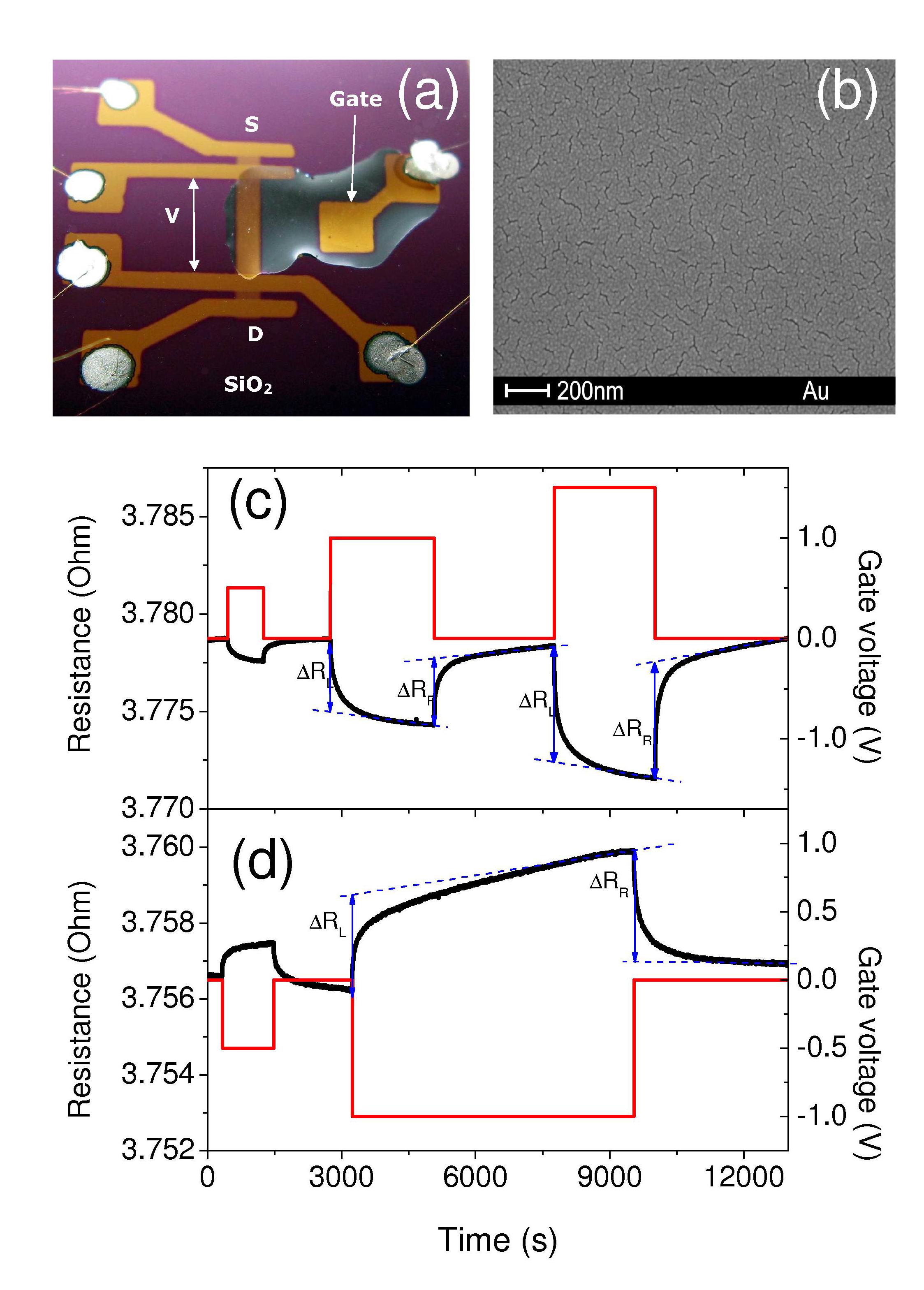
The field-effect devices were then mounted in a pulse-tube cryocooler and kept in high vacuum to protect the PES from moisture and chemical contaminations. Figures 1(c) and (d) show the effect of positive and negative voltage steps (applied at K, above the glassy transition of the polymer that occurs at about 210 K) on the resistance of the film, measured with the four-terminal technique with a DC current of 1-5 mA and by inverting the current to eliminate thermoelectric effects. The film resistance is related to the applied voltage through the charge on the EDL. For a given gate voltage the resistance variation (where ) is obtained by averaging the resistance jumps and on applying and removing the gate voltage, as shown in fig. 1.
The problem then arises of how to relate the gate voltage to the charge of the EDL and thus the density of the surface charge injected in the film. Hall-effect measurements would require huge magnetic fields because of the high intrinsic carrier density of Au. Moreover, determining the charge of the EDL by integrating the gate current is not correct if electrochemical effects are present, as pointed out in ref. Yuan10 . Electrochemical Impedance Spectroscopy (EIS) measurements carried out both on our devices and on a steel/PES/steel cell showed indeed that electrochemical effects take place at frequencies below 10 Hz Yuan10 . We thus used a procedure called double-step chronocoulometry Inzelt10 that allows separating the electrostatic charge we are interested in from the charge that flows through the PES because of electrochemical effects (e.g. diffusion of electroreactants).
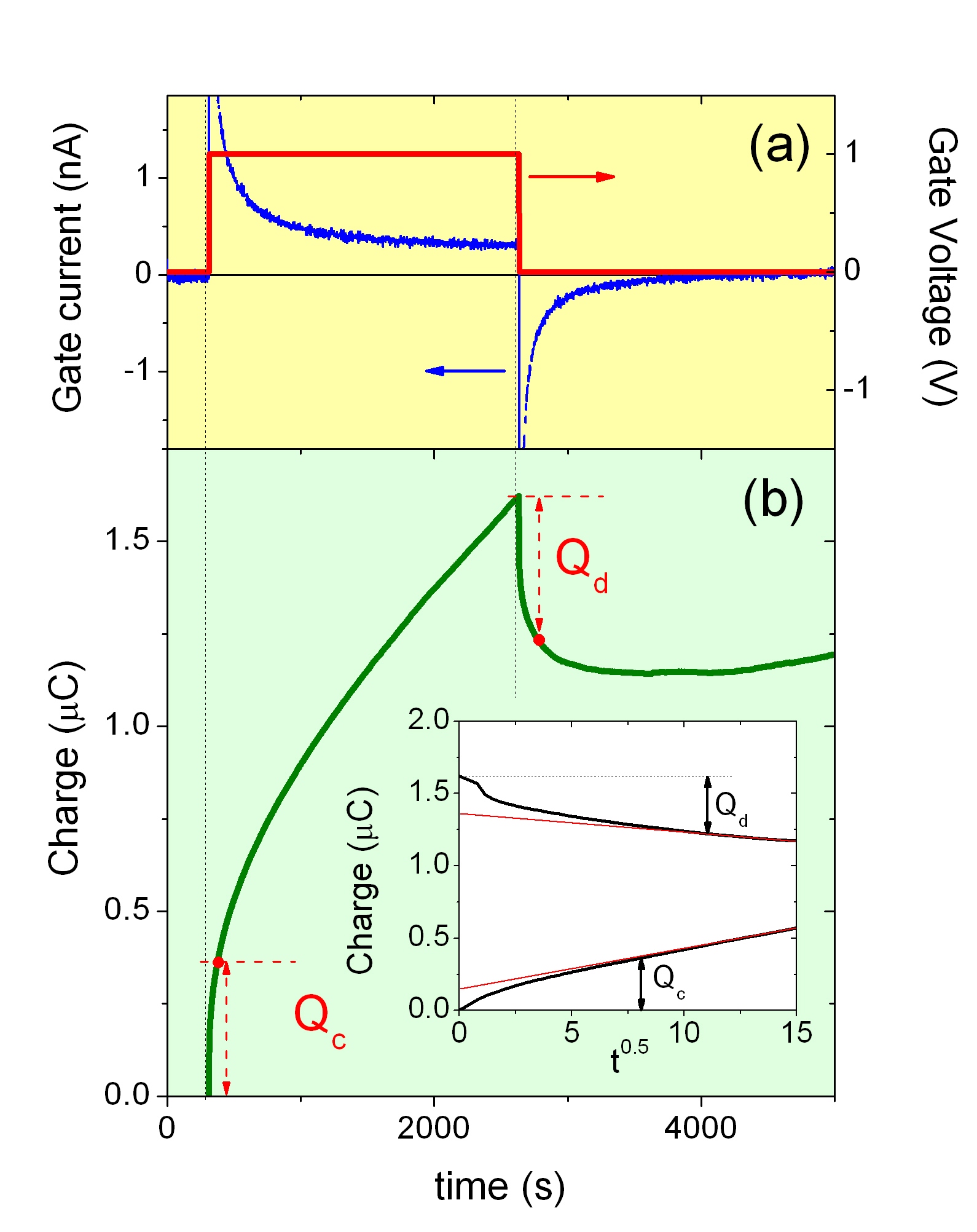
Figure 2 shows the time dependence of the gate current (a) and of the total charge (b) when a gate voltage of 1 V is applied and then removed. The curves are very similar to the typical ones depicted in Inzelt10 . Note that, after the first voltage step, a non-vanishing gate current continues to flow indefinitely. This current is due to the flow of charges necessary to maintain the gradient of ion concentration when tunneling effect through the EDL Yuan10 or diffusion of electroreactants Inzelt10 take place. The shape of shows indeed that two phenomena occur on very different length scales: a rather fast EDL charging/discharging (that gives an exponential time dependence) and other effects of electrochemical nature that give a dependence. In analogy with the chronocoulometry method, we determined the time at which starts to become linear as a function of , as shown in the inset to Fig.2(b), and assumed that the total charge “injected” in the film surface is . Clearly, two values are obtained, and , for the charge and discharge phases. Normally, they coincide within the experimental uncertainty; this indicates that no adsorption of reactants or product occurs Inzelt10 . The injected charge is finally defined as . In the few cases where deviates from the aforementioned behavior in one of the two steps (charge or discharge), is determined by the other step.
Once is known, the surface density of injected carriers is , where is the surface of the film covered by the polymer (gated area) and is the electronic charge.
Obviously, the charge distribution on the surface is not exactly 2D. Within the simplest semiclassical model one can imagine that the whole charge is injected in a surface layer (whose thickness is of the order of the screening length) and that the film behaves as the parallel of the perturbed and unperturbed regions. A trivial free-electron calculation (assuming constant effective electron mass and relaxation time) of the resistance of the whole film gives
| (1) |
where is the unperturbed 3D density of charge carriers. In this equation, does not depend explicitly on , but only on the whole film thickness and, of course, on . A more sophisticated perturbative self-consistent quantum approach based on the Lindhard-Hartree theory of the electronic screening Omini and including a proper model of the film conduction (e.g, accounting for the probability of electronic specular reflection at the film surface Fuchs38 ) gives a similar equation, but with an additional factor that depends in a complicated way on and . This term reduces to 1 when . Further details will be given elsewhere Omini .
Figure 3 shows that, for the great majority of the devices studied here, is a linear function of , in agreement with eq. 1 111The thickness of the thinner film (5 nm) results from a correction that accounts for the voids in polycrystalline films that reduce the actual film cross section (see ref.Rowell03 ). In the other cases the correction was not necessary.. Vertical and horizontal error bars account for the difference in the values of and determined in the charging and discharging phases – i.e. on application and removal of the gate voltage, see fig.1 (c,d) and the inset to fig.2(b).
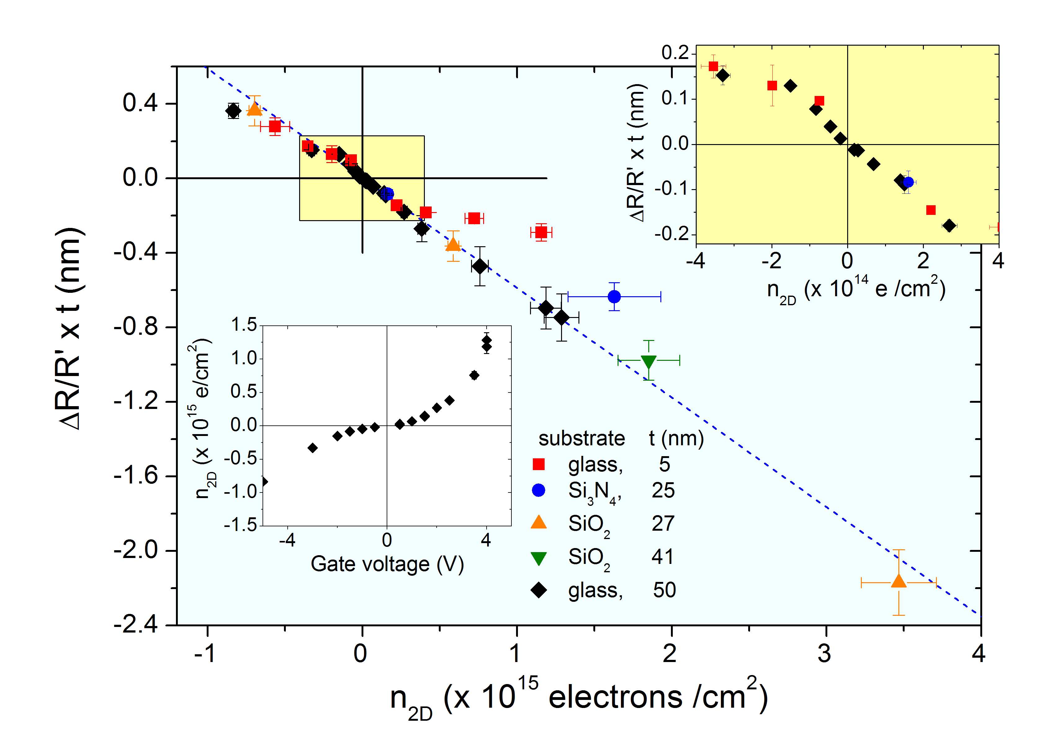
Note that the values of reported so far in literature are included in the yellow region around the origin of the axes. A magnification of this region is shown in inset. The values of obtained with our technique extend instead up to electrons/cm2. The same linear trend is common to all devices, but some deviations occur in the thinner ones at higher charge densities. This is not surprising since in these films the surface scattering plays a major role, and the simple free-electron model (eq. 1) breaks down. A reduction in the absolute value of for a given is indeed predicted by the aforementioned quantum perturbative model Omini when the probability of electron reflection at the surface Fuchs38 is not negligible.
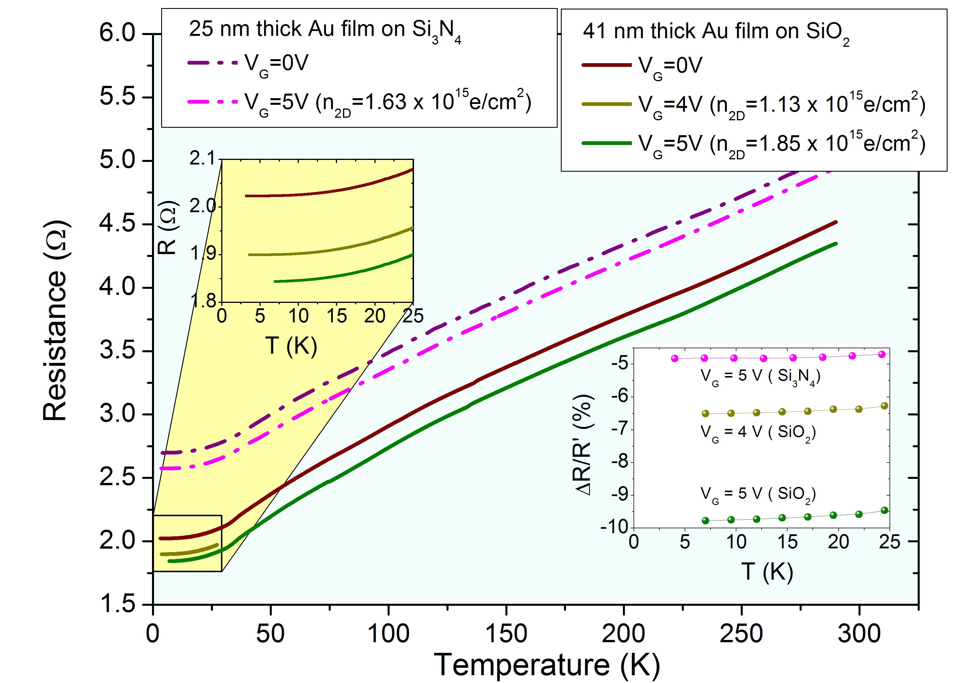
In view of the application of this gating technique to more interesting 2D materials, like graphene and multilayer graphene, graphane Giustino10 , MoS2, BN, NbSe2 and so on – in particular to see whether some of these materials can develop superconductivity upon charge doping – it is important to check what happens when the device is cooled to cryogenic temperatures. Because of the glassy transition of the polymer at K, and the consequent “freezing” of the EDL charge below that threshold, the gate voltage must be applied at and kept constant on cooling. As expected, the gate current that persists after the EDL charge (see fig.2(a)) and that is related to the ionic flow in the polymer electrolyte goes smoothly to zero on crossing the glassy transition. The cooling speed should be small enough to avoid cracks in the film or in the contacts due to the abrupt thermal contraction of the polymer. The resistance of the film is then measured on slowly heating the FED from the lowest temperature (here about 3.3 K) to room temperature. Figure 4 shows the curves for two Au films on different substrates, i.e. Si3N4 (dash-dot lines) and SiO2 (solid lines). The curves at and V are shown for both devices; for the latter, an additional curve at V is reported, though it extends only up to 28 K because one of the contact broke down at that temperature. A large offset is observed within each series, due to the applied field. The inset shows the low-temperature values of extracted from these curves. At the lowest temperatures, the resistance varies by almost 10%, which is a huge quantity for a noble metal. Incidentally, preliminary measurements on Cu films indicate an even larger effect (up to 30%).
Finally, fig. 5 reports and compares in log-log scale some results obtained in Au devices of different kinds, i.e. based on PESs with different compositions, and also in conventional back-gate field-effect devices made by depositing the Au film and the electrodes on top of a suspended SiN membrane Delaude09 with the Au gate electrode on the other side. The figure clearly shows that is a linear function of for all kinds of devices; the vertical offset of the parallel trend lines is mainly due to the different thickness of the films.
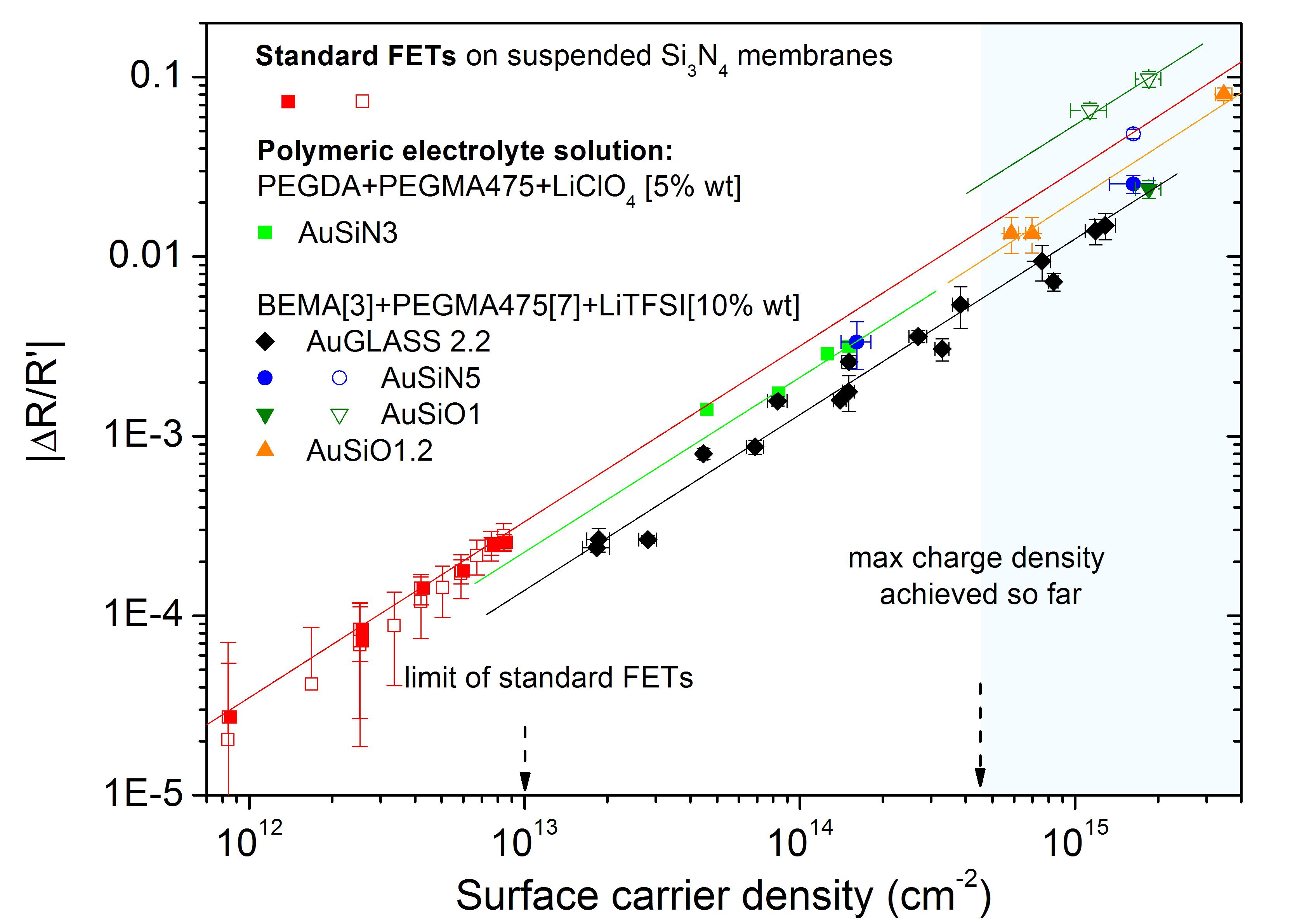
In conclusion, we have shown that with a suitable polymeric electrolyte solution it is possible to extend the range of surface charge densities achieved in field-effect experiments (even at cryogenic temperatures) to some units in charges/cm2. These values are well in the range where giant modulations of the conduction properties of some 2D materials, and even the occurrence of superconductivity (e.g. in graphane Giustino10 ) are expected. For the time being, we have shown that these huge carrier injections give rise to large variations in the resistance of Au thin films, up to about 10%. The quantity for a given device linearly depends on , while all the data follow a universal linear trend if a proper normalization to the film thickness is used. Some deviations are observed in very thin films, where the free-electron model is unable to describe the conduction. These deviations are however compatible with more sophisticated perturbative quantum models.
References
- (1) R. E. Glover, III and M. D. Sherrill, Phys. Rev. Lett. 5, 248 (1960).
- (2) J. Mannhart et al., Z. Phys. B 83, 307 (1991).
- (3) C. H. Ahn et al., Science 284, 1152 (1999).
- (4) H. Shimotani et al., Appl. Phys. Lett. 91, 082106 (2007)
- (5) K. Ueno et al., Nature Mater. 7, 855-858 (2008).
- (6) J. T. Ye et al., Nature Mater. 9, 125-128 (2009).
- (7) K. Ueno et al., Nature Nanotechnology 6, 408 (2011).
- (8) M. J. Panzer, C. R. Newman, and C. D. Frisbie, Appl. Phys. Lett. 86, 103503 (2005)
- (9) A. S. Dhoot et al., Proc. Natl. Acad. Sci. 32, 11834-11837 (2006).
- (10) H. T. Yuan et al., Adv. Funct. Mater. 19, 771-774 (2009).
- (11) G. Bonfiglioli and R. Malvano, Phys. Rev. 115, 330 (1959).
- (12) G. Bonfiglioli and R. Malvano, Phys. Rev. 101, 1281 (1965).
- (13) H.L. Stadler, Phys. Rev. Lett. 14, 979 (1965)
- (14) G. Martinez-Arizala et al., Phys. Rev. Lett. 78, 1130 (1997)
- (15) N. Marković et al., Phys. Rev. B 65, 012501 (2001).
- (16) L. Zhang et al., Surface Science, 439, 73 (1999).
- (17) H. Yuan et al., J. Am. Chem. Soc. 132, 18402 (2010).
- (18) G. Inzelt, in Electroanalytical Methods. Guide to Experiments and Applications, edited by F. Scholz, Springer-Verlag 2010, p. 147.
- (19) M. Omini et al., unpublished.
- (20) K. Fuchs, Proc. Cambridge Philos. Soc. 34, 100 (1938)
- (21) J.M. Rowell, Supercond. Sci. Technol. 16, R17 (2003)
- (22) G. Savini, A. C. Ferrari, and F. Giustino, Phys. Rev. Lett. 105, 037002 (2010).
- (23) D. Delaude, Ph.D. Thesis, unpublished (2009).