Electrolyte gate-controlled Kondo effect in SrTiO3
Abstract
We report low-temperature, high-field magnetotransport measurements of SrTiO3 gated by an ionic gel electrolyte. A saturating resistance upturn and negative magnetoresistance that signal the emergence of the Kondo effect appear for higher applied gate voltages. This observation, enabled by the wide tunability of the ionic gel-applied electric field, promotes the interpretation of the electric field-effect induced 2D electron system in SrTiO3 as an admixture of magnetic Ti3+ ions, i.e. localized and unpaired electrons, and delocalized electrons that partially fill the Ti conduction band.
pacs:
72.15.Qm, 75.20.Hr, 75.47.-mThe Coulomb interaction amongst electrons and ions in a solid can spontaneously generate internal magnetic fields and effective magnetic interactions. Unexpected magnetic phenomena may emerge whenever we consider a new system where interactions are important. In recent years, predictions for and observations of magnetism originating in the two-dimensional (2D) system of electrons at the interface between SrTiO3 (STO) and LaAlO3 (LAO) have attracted much attention Pentcheva2006 ; Nanda2011 ; Brinkman2007 ; Dikin2011 ; Huijben2009 ; Li2011 , particularly the prediction of charge disproportionation and the emergence of -valent Ti sites with unpaired spin Pentcheva2006 and direct measurements of in-plane magnetization Li2011 . The conducting electrons at the LAO/STO interface are believed to be induced by polar LAO’s strong internal electric fields, and to reside on the Ti sites on the STO side of the interface, partially filling the lowest-lying Ti bands Nakagawa2006a ; Salluzzo2009 ; Schlom2011 . Questions remain, however, over the role of the growth process, in particular whether oxygen vacancy formation or cation intermixing are in fact responsible for the observed -type conduction Siemons2007 ; Herranz2007 ; Willmott2007 ; Kalabukhov2011a .
Other than growing a polar overlayer, a 2D system of electrons in STO can be made by chemical doping with Nb, La, or oxygen vacancies Kozuka2009a ; Son2010 ; Jalan2010 ; Santander-Syro2011 , or purely electrostatic charging in an electric double layer transistor (EDLT) Ueno2008 ; Lee2011b . If electronic reconstruction in response to overlayer polarity is an accurate description for LAO/STO, then that system can be closely modeled by field effect-induced electrons in undoped STO, where confounding questions over growth conditions do not arise, and the applied electric field can be widely tuned.
In this Letter, we expand on the body of evidence for Ti3+ magnetism in STO that conducts in two dimensions. We demonstrate a gate-controlled Kondo effect in the 2D electron system in undoped STO formed beneath the bare surface by the electric field from an ionic gel electrolyte, and interpret this system as an admixture of magnetic Ti3+ ions (unpaired and localized electrons) and delocalized electrons partially filling the Ti conduction band, as predicted theoretically Popovic2008 ; Nanda2011 . The Kondo effect is an archetype for the emergent magnetic interactions amongst localized and delocalized electrons in conducting alloys Kondo1964 ; Gruner1974 , and the ability to produce and tune the effect by purely electrostatic means in any conducting system is of interest in its own right Goldhaber-Gordon1998a ; Chen2011 . The observed appearance of the Kondo effect in STO as a function of applied electric field points to the emergence of magnetic interactions between electrons in STO due to electron-electron correlations rather than the presence of dopants.

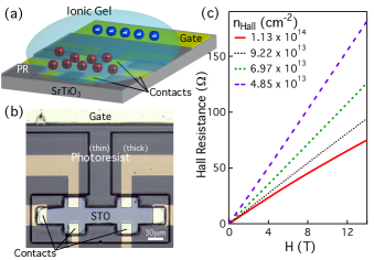
We report measurements from two STO Hall bar devices (A and B), gated using an ionic gel electrolyte in an EDLT configuration. Behaviors similar to those we show have been observed in 6 devices. A schematic showing the operation of the devices is shown in Fig. 1(a), and a photograph of a device identical to those we measured but without the electrolyte is shown in Fig. 1(b). Undoped STO (100) crystals (MTI Corp.) were treated with buffered hydrofluoric acid to obtain a TiO2-terminated surface Kawasaki1994 , and the crystal for device B was then annealed at in a tube furnace with 50 sccm of flowing oxygen gas. The Hall bar geometry, wide and long between the voltage leads, was defined via a window through a 1 m-thick film of hard-baked photoresist that exposes the channel and the gate to the electrolyte while keeping the rest of the STO separated from the ions and hence still insulating. Prior to the lithographic definition of the Hall bar, contacts were created by Ar+ ion milling to a dose of with acceleration Reagor2005 then depositing Al/Ti/Au electrodes with thickness of 40/5/100 nm. The ionic gel electrolyte was formed by gelation of a triblock copolymer poly(styrene-block-methylmethacrylate-block-styrene) (PS-PMMA-PS) in an ionic liquid 1-ethyl-3-methylimidazolium bis(trifluoromethanesulfonyl)amide (EMI-TFSA, formerly referred to as EMI-TFSI) Cho2008 ; Lee2009 . A drop of gel was formed on another substrate, then manually pasted over the device, covering both the STO channel and the coplanar metal gate.
Magnetotransport characteristics of device A were measured in a Physical Property Measurement System (Quantum Design) at temperatures down to and magnetic fields up to . The sample was insulating at the start and the end of the experiment, indicating that the conduction was not due to doping by electrochemical reactions. At room temperature, the gate voltage was ramped up to , which polarized the electrolyte, pushing cations toward the channel. The electric field of the ions cause the accumulation of electrons that form our 2D system in STO. Then the sample was cooled to , during which the leakage current through the gate dropped below the measurement limit of for , signaling the freezing of EMI-TFSA. Once at , was nulled and magnetotransport measurements were taken. To apply a weaker electric field and set the electron density lower, the device was warmed to , and the electrolyte was allowed to partially lose its polarization, decreasing the accumulated cation concentration at the channel and correspondingly the electron density in the STO.
We measured the longitudinal resistance of the device as a function of temperature and applied magnetic field, using standard lock-in techniques at quasi-DC frequencies with a current bias and no additional source-drain bias. Figure 1(c) shows Hall resistance measurements at that show that the electron density inferred from Hall effect decreases for each successive cooldown, from in the first cooldown, to for the last. We have measured densities as high as in some other samples, but the devices described here with showed lower disorder and have the observed density and other transport features most similar to other high-mobility 2D systems in STO.
The 2D nature of our samples is evident from three magnetoresistance features which have not been reported in previous EDLT studies of STO: the dependence of the Hall resistance as a function of , weak anti-localization, and Shubnikov-de Haas oscillations (See Supplementary Information). Weak anti-localization with similarly strong spin-orbit coupling strengths has been reported in the LAO/STO interface and attributed to the Rashba-type coupling due to inversion asymmetry of the interface Caviglia2010a . Shubnikov-de Haas oscillations were seen in device B at , which gave . The electron density inferred from the oscillation period was much lower at if only a twofold spin degeneracy is assumed (See Supplementary Information). Reported quantum oscillations of the magnetoresistance in LAO/STO and -doped STO have yielded similarly low values of the inferred electron density Caviglia2010 ; BenShalom2010a ; Kozuka2009a ; Jalan2010 .

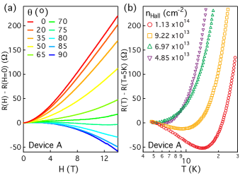
The magnetoresistance of the sample, , measured at the highest electron density, is plotted in Fig. 2(a) for various directions of . When is normal to the sample plane (), the magnetoresistance is positive, and as the direction is tilted away from normal and into the sample plane, the magnetoresistance crosses over from positive to negative at . A similar crossover from positive out-of-plane magnetoresistance to negative in-plane magnetoresistance has been reported in LAO/STO Shalom2009 .
We pay particular attention to the sample’s zero-field resistance as a function of temperature, . Fig. 2(b) shows the resistance relative to its value at , , at each measured electron density. At the highest density, a minimum is seen at and the resistance turns upward, and this upturn is substantially weakened as the density is lowered. The appearance of a resistance minimum and low-temperature upturn, unexpected for a metallic system, at higher electron density suggests that the electric field-induced electrons, not added impurities, are themselves responsible for the scattering, and electron-electron correlations strongly influence the transport properties. A disorder-induced metal-insulator transition, by contrast, ought to show a stronger upturn at lower density, not the opposite trend seen here. The precise threshold density for the emergence of an minimum differs amongst samples, but the overall trend is the same. Reducing the induced 2D electron density reduces the low-temperature upturn in resistance.
To further investigate these anomalies we measured device B at lower temperatures down to and higher magnetic fields up to . We set for the first cooldown and measured at . To set lower densities for subsequent cooldowns, we set lower at then waited for minutes for the electrolyte to equilibrate, rather than nulling and quickly obtaining a partial loss of polarization as described above for device A.
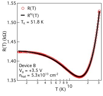
Figure 3 shows the device B zero-field at , corresponding to the highest electron density measured in this sample. A minimum of is seen at , and then the upturn saturates at the lowest temperatures, such that for . This saturating resistance upturn is suppressed in subsequent cooldowns at lower gate voltages, and thus the same overall trend in the behavior of with respect to electron density is observed in both devices. Finally in the last cooldown and lowest density, a non-saturating upturn and localization-like behavior is observed (See Supplementary Information).

The appearance of a saturating resistance upturn at low temperature is characteristic of the Kondo effect, where the temperature dependence of the contribution from magnetic impurities to the electrical resistivity of a metal is a universal function in units of a single temperature scale, the Kondo temperature . This universal function behaves logarithmically at high temperature , and saturates at low temperature, so that for if we define as the temperature at which the Kondo resistivity is half relative to its zero-temperature value Kondo1964 ; Costi1994 . Across the whole measured temperature range from to which includes temperatures above and below the observed minimum, the resistance can be described well by a simple Kondo model
| (1) |
where is the residual resistance due to sample disorder, and the and terms represent the functional temperature dependences of the electron-electron and the electron-phonon interactions, respectively. For the numerical fitting of this model to the data, we used an empirical form for the universal resistivity function,
| (2) |
where , and we fixed to closely match the theoretical result obtained by the numerical renormalization group Costi1994 ; Goldhaber-Gordon1998 . A numerical fit using Eqns. 1 and 2 to the measured curve yielded , , , , and .
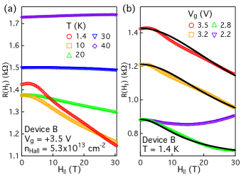
Device B, with applied parallel to sample plane and , also exhibited a strong negative magnetoresistance, up to at , and its is plotted in Fig. 4. The temperature-dependent magnetoresistance at , plotted in Fig. 4(a), shows that raising the sample temperature suppresses the negative in-plane magnetoresistance such that the effect disappears between 30 and . In the highest fields , the Kondo resistance upturn is sufficiently suppressed that resistance depends monotonically on temperature. Such a temperature dependence of the magnetoresistance is expected from the splitting of the Kondo Peak in the spectral function by an applied magnetic field, which leads to negative magnetoresistance by suppressing the Kondo effect on resistance Felsch1973 ; Costi2000 .

Measurements of were done at each gate voltage at the lowest temperature , and the results are plotted in Fig. 4(b) along with their comparison to a simple Kondo model
| (3) |
where now is the universal function for zero-temperature magnetoresistivity of a Kondo impurity, related to its magnetization which may be calculated using Bethe-Ansatz techniques, and is a magnetic scale, related to the Kondo temperature and the -factor of the impurity spin Andrei1983 . To compare the data and model we numerically evaluated the exact form of (See Supplementary Information and Andrei1983 ) and chose to compare with the data obtained at , respectively. The comparison is not exact and fails for low fields, where weak anti-localization and other effects may be relevant, but the overall dependence and shape are broadly consistent, particularly for the lower density at .
The negative in-plane magnetoresistance is suppressed as the electron density is lowered, once again implying that the observed Kondo effect originates from the electrons accumulated at the surface due to the applied electric field of the electrolyte gate. As the Kondo effect arises due to the interaction between localized and delocalized electrons, we can interpret our observations by viewing the 2D electron system as an admixture composed of localized and unpaired electrons—perhaps polaronic in nature Nanda2011 —that act as the Kondo scattering centers and a metal of delocalized electrons that partially fill the Ti conduction band.
Finally, we comment on the implications of the results described herein for the ongoing efforts to conclusively understand the LAO/STO interface, where an minimum and negative magnetoresistance have already been reported Brinkman2007 . By electrostatically inducing 2D electrons in STO, we have modeled the essential physics of the polar catastrophe, and the demonstration of a gate-controlled Kondo effect in undoped STO shows that the observations of electronic conduction and magnetism in LAO/STO are plausibly due to electronic reconstruction and are not necessarily a result of unintended doping during LAO growth Huijben2009 ; Schlom2011 . The magnetic interactions found in STO, added to its other attractive features including tunability of the ground state by applied electric fields and superconductivity, show STO-based interfaces and heterostructures to be a promising playground in which to look for and study emergent electronic phenomena and novel device applications Takagi2010a ; Mannhart2010 .
Acknowledgements.
We thank J. Jaroszynski, S. Stemmer, B. Jalan, I. R. Fisher, J. G. Analytis, M. Chalfin, E. Eason, Y. Cui, J. J. Cha, Y. Lee, and T. A. Costi. The development of ionic gating technique was supported as part of the Center on Nanostructuring for Efficient Energy Conversion, an Energy Frontier Research Center funded by the U.S. Department of Energy, Office of Science, Office of Basic Energy Sciences under Award Number DE-SC0001060. The measurement and study of STO were supported by the MURI program of the Army Research Office Grant No. W911-NF-09-1-0398. The Minnesota contribution was supported by the National Science Foundation through the MRSEC program at the University of Minnesota, Award DMR-0819885. ML is partially supported by Samsung Scholarship and the Stanford Graduate Fellowship. A portion of this work was performed at the National High Magnetic Field Laboratory, which is supported by National Science Foundation Cooperative Agreement No. DMR-0654118, the State of Florida, and the U.S. Department of Energy.References
- (1) R. Pentcheva and W. Pickett, Phys. Rev. B 74 035112 (2006).
- (2) B. Nanda and S. Satpathy, Phys. Rev B 83, 195114 (2011).
- (3) A. Brinkman et al., Nat. Mater. 6, 493 (2007).
- (4) D. A. Dikin et al., Phy. Rev. Lett. 107, 056802 (2011).
- (5) M. Huijben et al., Adv. Mater. 21, 1665 (2009).
- (6) L. Li et al., arXiv:1105.0235.
- (7) N. Nakagawa, H. Y. Hwang, and D. A. Muller, Nat. Mater. 5, 204 (2006).
- (8) M. Salluzzo et al., Phys. Rev Lett. 102, 166804 (2009).
- (9) D. G. Schlom and J. Mannhart, Nat. Mater. 10, 168 (2011).
- (10) W. Siemons et al., Phys. Rev Lett. 98, 196802 (2007).
- (11) G. Herranz et al., Phys. Rev. Lett. 98, 216803 (2007).
- (12) P. Willmott et al., Phys. Rev. Lett. 99, 155502 (2007).
- (13) A. Kalabukhov et al., Europhys. Lett. 93, 37001 (2011).
- (14) Y. Kozuka et al., Nature 462, 487 (2009).
- (15) J. Son et al., Nat. Mater. 9, 482 (2010).
- (16) B. Jalan et al., Phys. Rev. B 82 081103 (2010).
- (17) A. F. Santander-Syro et al., Nature 469, 189 (2011).
- (18) K. Ueno et al., Nat. Mater. 7, 855 (2008).
- (19) Y. Lee et al., Phys. Rev. Lett. 106, 136809 (2011).
- (20) Z. Popovic, S. Satpathy, and R. Martin, Phys. Rev. Lett. 101, 256801 (2008).
- (21) J. Kondo, Prog. Theor. Phys. 32, 37 (1964).
- (22) G. Gruner and A. Zawadowski, Reports on Prog. in Physics 37, 1497 (1974).
- (23) D. Goldhaber-Gordon et al., Nature 391, 156 (1998).
- (24) J.-H. Chen et al., Nat. Phys. 7, 535 (2011).
- (25) M. Kawasaki et al., Science 266, 1540 (1994).
- (26) D. W. Reagor and V. Y. Butko. Nat. Mater. 4, 593 (2005).
- (27) J. H. Cho et al., Nat. Mater. 7, 900 (2008).
- (28) J. Lee et al., J. Phys. Chem. C 113, 8972 (2009).
- (29) A. D. Caviglia et al., Phys. Rev. Lett. 104, 126803 (2010).
- (30) A. D. Caviglia et al., Phys. Rev. Lett. 105, 236802 (2010).
- (31) M. Ben Shalom et al., Phys. Rev. Lett. 105, 206401 (2010).
- (32) M. Ben Shalom et al., Phys. Rev. B 80, 140403 (2009).
- (33) T. A. Costi, A. C. Hewson, and V. Zlatic, J. of Phys.: Condens. Matter 6, 2519 (1994).
- (34) D. Goldhaber-Gordon et al., Phys. Rev. Lett. 81, 5225 (1998).
- (35) W. Felsch and K. Winzer, Solid State Commun. 13, 569 (1973).
- (36) T. Costi., Phys. Rev. Lett. 85, 1504 (2000).
- (37) N. Andrei, K. Furuya, and J. Lowenstein, Rev. Mod. Phys. 55, 331 (1983).
- (38) H. Takagi and H. Y. Hwang, Science 327, 1601 (2010).
- (39) J. Mannhart and D. G. Schlom, Science 327, 1607 (2010).