Tunable quantum spin Hall effect in double quantum wells
Abstract
The field of topological insulators (TIs) is rapidly growing. Concerning possible applications, the search for materials with an easily controllable TI phase is a key issue. The quantum spin Hall effect, characterized by a single pair of helical edge modes protected by time-reversal symmetry, has been demonstrated in HgTe-based quantum wells (QWs) with an inverted bandgap. We analyze the topological properties of a generically coupled HgTe-based double QW (DQW) and show how in such a system a TI phase can be driven by an inter-layer bias voltage, even when the individual layers are non-inverted. We argue, that this system allows for similar (layer-)pseudospin based physics as in bilayer graphene but with the crucial absence of a valley degeneracy.
pacs:
73.20.-r, 73.43.-f, 73.21.Fg, 73.61.-rSince the understanding of the topological nature of the quantum Hall effect Laughlin (1981); Thouless (1982), topological phases have become one of the most active research fields in condensed matter physics. More recently, a new topological phase preserving time-reversal symmetry (TRS), the quantum spin Hall (QSH) phase Kane and Mele (2005a, b) has been discovered. The QSH phase has been theoretically predicted Bernevig et al. (2006) and experimentally realized in 2D HgTe/CdTe QWs König et al. (2007). The crucial ingredient of this narrow gap semiconductor material is strong spin-orbit coupling, which determines the inverted band structure of HgTe. The experimentally accessible parameter tuning the band structure from normal (CdTe-like) to inverted is the thickness of the HgTe QW. One year later, 3D TIs supporting chiral fermions as surface states have been proposed and observed Fu and Kane (2007); Hsieh et al. (2009a); Zhang et al. (2009); Hsieh et al. (2009b); Xia et al. (2009); Chen et al. (2009). These two phenomena are examples of the general concept of a TI which is a TRS preserving system with a bulk insulating gap which features topologically protected edge states due to the Atiyah-Singer index theorem which is in this context referred to as the bulk boundary correspondence. TI phases are characterized by a topological invariant Kane and Mele (2005a); Moore and Balents (2007).
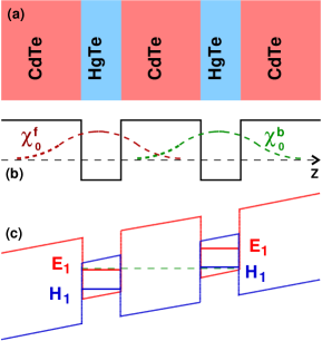
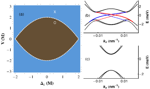
In this work, we extend the Bernevig-Hughes-Zhang (BHZ) model Bernevig et al. (2006) to account for a double QW (DQW) of HgTe (see Fig. 1). We analyze how the topological features of the DQW depend on a generic tunneling Hamiltonian effectively connecting the two wells and on the applied voltage between them. In particular, we show that a QSH phase can be driven by also when the two QWs are individually trivial. We also derive a reduced 2-band model that well captures the topological features of the system. We give analytical expressions of the effective parameters that map the reduced model to the BHZ-model of a single HgTe QW [in Eq. (10)] as a function of the tunneling matrix elements and voltage . We show that a non-trivial topological invariant is accompanied with the appearance of a single pair of helical edge states for which we calculate the energy dispersion and spinors. In Fig. 2(a) we show the phase diagram of the model as a function of tunneling amplitude and applied voltage.
I Double quantum well model
The system under investigation consists of a DQW of HgTe as shown in Fig. 1, which can be thought of as a 2D TI bilayer. The system is contacted to gates that control the potential bias between the front (f) and back (b) QWs. The spectrum of a single HgTe-based QW near the -point is effectively described by the BHZ model Bernevig et al. (2006)
| (3) | |||||
| (4) | |||||
where are the Pauli matrices pauli associated with the band-pseudospin degree of freedom (band or ). is represented in the basis , , , , where the states () are a mixing of the s-like band with the light-hole band, while () is basically the heavy-hole band sym . In the following we will use the parameter values meV nm, eV and meV , estimated by a comparison with the Kane Hamiltonian Novik et al. (2005), and assume without loss of generality. The Dirac rest mass depends on the QW thickness and corresponds to the inverted (QSH) regime whereas corresponds to the normal regime. In first approximation, is block diagonal in the Kramer’s partner or spin degree of freedom Bernevig et al. (2006) (with the vector of Pauli matrices). Because we consider only systems with TRS, we restrict ourselves to the block , from which the results can be extended to the other one by applying the time reversal operator .
The Hamiltonian in Eq. 4 describes the in-plane electronic motion inside a QW layer. Along the confinement direction of the QW (), electrons are described by the envelope function (integrated out in the BHZ model). When the two QWs of a DQW are sufficiently separated, an electron will be localized either on the f or on the b layer, with envelope function and , resp. When the two layers are placed close to each other, and acquire a finite overlap, accounted for by a tunneling Hamiltonian . This description should take into account that is a spinor with components on the and bands. To first order in , the tunneling Hamiltonian has the form
| (5) | |||||
where are Pauli matrices associated with the layer projection [layer pseudospin (LPS) ]. generates bonding/antibonding states with energy splitting ()note2 of the () band. The lowest order off-diagonal term is , due to the axial symmetry and the character of and bands sym . In the Appendix A, we present a realistic estimate of HgTe DQW tunneling parameters.
The DQW Hamiltonian for a single Kramer’s block is therefore
| (6) |
where is due to the possible variation of the parameters of between the f and the b layer. In particular, we consider , with the interlayer bias.
II Band structure and topology
The topological properties of a fully gapped 2D TRS preserving system are described by the -invariant Fu and Kane (2007). When the model Hamiltonian is block diagonal with respect to the Kramers partner spin , the system can be thought of, from a topological point of view, as two copies of an anomalous quantum Hall effect, related by time reversal Qi et al. (2006). Each of the blocks is topologically characterized by its first Chern number and resp., which we call the Kramers Chern numbers (KCNs). TRS immediately implies that the two KCNs obey a zero sum rule Avron et al. (1988), meaning . The invariant is then given by Qi et al. (2006)
| (7) |
with the KCN defined as
| (8) |
and where the Berry curvature is given by
| (9) |
where stands for the exterior product. The sum is over the occupied bands and are Bloch states of the Kramers block Hamiltonian. In order to make the Chern number well defined in local models, like Eq. 6, a lattice regularization has to be included to compactify the k-space. In our case, since the curvature decays rapidly away from the -point, the integral in Eq. (8) over the -space converges stably towards the KCN of the lattice regularized model.
Let us first analyze the bulk dispersion curves described by Eq. 6 to get an intuition for possible local topological phase transitions Budich and Trauzettel (2011) at the -point, induced by band crossings. For we obtain the four eigenenergies
| (10) |
with . Due to the interlayer tunneling, the bands (centered at ) suffer an energy splitting, at the -point, of , while for the bands (centered at ) the splitting is . We define a local energy gap (LEG) at as
| (11) |
When the LEG changes sign an inversion of bands with and character occurs at the -point, accompanied by a possible topological phase transition. For a fixed set of parameters, the condition defines (if existent) the critical value of the bias driving the phase transition:
| (12) |
This is confirmed by the explicit calculation of the -invariant with Eq. 7, as shown in Fig. 2, where we calculated the KCN , as a function of and . is insensitive to the value of , as long as and/or remains finite, in which case an insulating gap arises. Interestingly, for , lowest bulk bands have at small a Dirac-like dispersion, while a tunable gap is developed for . In the region , the system supports an even number of pairs of helical edge modes , in particular for and for . In the outer region, instead, the DQW is topologically non-trivial and allows for a pair of time-reversal protected helical modes. An example of the DQW spectrum in the two regimes, described by Eq. 6, is shown in Fig 2(b) and (c) (full lines) for a positive mass meV and a bias of meV and meV, resp. Edge states are obtained by numerically solving Eq. 6 with open boundary conditions.
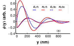
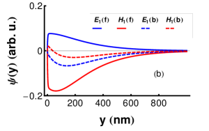
In Fig 3(a) and (b), we plot the wave function of the helical edge states for meV (near the Dirac point) and meV (near the valence bands), resp. for the system in Fig. 2(b). These states have the peculiarity of supporting at the same time both oscillatory and decaying behavior [clearly evident in Fig 3(a)], due to the contribution of modes with complex , which is related to the Mexican hat shape of the bulk bands. Approaching the bulk bands, the oscillations tend to become less pronounced, as shown in Fig 3(b). The edge modes have the major contribution from the band of the f layer, which consists in of the probability weight near the conduction band and rises to near the valence band. Under the reversal of , the probability weights of the b and f layer interchange.
III Reduced Hamiltonian
In order to get an analytical understanding of the system, we derive a reduced 2-band low-energy Hamiltonian , with the assumption that the relevant energies are small compared to . is represented in the basis or for the and sign, resp. Similar to BLG, we separate the DQW Hamiltonian in Eq. 6 in a low-energy and a high-energy part connected by the off-diagonal blocks . The reduced 2-band model is obtained then as , where McCann and Fal’ko (2006). The reduced model can be mapped to a TI Hamiltonian of a single layer (Eq. 4), but with the renormalized parameters
| (13) |
while remains unchanged. The bulk dispersion is characterized by a Mexican hat dispersion for , where , with a gap . If the condition for the existence of the Mexican hat is not fulfilled, the dispersion has a minimum at and a gap of . For a barrier thickness of nm, we obtain meV (see Table 2 in the Appendix for details), which does not strongly depend on . This suggests that the parameters obtained are in the correct ballpark for experiments.
The bulk dispersion curves are quite well reproduced by , as demonstrated in Figs. 2(b) and (c) (black dashed lines). However, predicts edge modes with purely linear dispersions , where denotes the two spin-blocks [colored dashed lines in Figs. 2(b)]. Instead, edge dispersions numerically obtained from the full model [colored full lines in Figs. 2(b)] show a marked non-linear behavior when approaching the bulk bands, with an accompanying shift of the Dirac point.
For the reduced model the KCN can be calculated analytically since assumes the simple form Bernevig et al. (2006)
| (14) |
where is the unit vector of . The topological features of are therefore analogous to those of a single layer of 2D TI. However, the bias voltage enters the Dirac mass parameter thus providing an additional knob to tune a system of two trivial insulators into a single-valley Dirac system ) and eventually into a nontrivial TI phase. Since the phase transition at is local at the -point Budich and Trauzettel (2011) the analytical topological predictions of the reduced model are inherited by the full model and survive a lattice regularization which makes the KCN mathematically well defined.
Finally, we note that the proposed mechanism of a voltage bias induced band inversion in a DQW is by no means restricted to HgTe based QWs. The method in principle even applies to large band gap semiconductors like GaAs ( eV) but the presumably large inversion asymmetry, not captured in our model, would have to be taken into account explicitly.
IV Discussion and conclusion
It has been proposed earlier that, in single QWs, the topological phase transition may be induced by an effective applied potential Yang et al. (2008); Liu et al. (2008); Li and Chang (2009). In Refs. Yang et al., 2008; Li and Chang, 2009, calculations show that in a single Hg1-xCdxTe QW, a potential bias along the well thickness of the order of hundreds of meV [much larger than needed in our proposal (on the order of a few meV)] induces a band inversion. The experimental feasibility of this approach is arduous due to the large field required. In Ref. Liu et al., 2008, a type-II quantum well made of InAs/GaSb/AlSb, which has an intrinsically inverted bandstructure, is considered. The authors show that the spatial separation of E1 and H1 bands offers a key to drive the transition from the TI to the normal phase with an applied gate bias. Recent experiments knez et al. (2011a, b) provided the first evidences pointing towards the presence of a TI phase in these kind of structures. The proposal in Ref. Liu et al. (2008) requires the growth of a type-II QW, which is a strongly asymmetric structure interfacing two specifically chosen semiconducting materials with different electron affinities (InAs and GaSb). On the contrary, we envision a DQW with each well made from the same material that might be more feasible to experimentally realize clean samples and offers the possibility of tuning the tunneling parameters by modifying the barrier thickness or its chemical composition. This tunability could also be used to create contacts between two helical Luttinger liquids when each QW is in the non-trivial regime and . This contact can be either of electrostatic nature which allows to study Coulomb drag drag or a new type of inter-edge correlated liquid contacthelical , or can induce the tunneling between helical edge states combiedge .
Further, we note that the LPS () [see Eq. (2)], that operates on the wave function amplitude on the and layers, can be manipulated by the various parameters, in particular by the voltage . As already mentioned, in the regime , the low-energy physics of the DQW is described by Eq. (1), with parameters from Eq. (10), where the basis is given by eigenstates of the LPS with eigenvalues and resp. If in Eq. (10) is zero, points in-plane for small in-plane -vector and has a Berry phase of like in graphene. A finite mass tilts out-of plane and starts to localize in one of the layers. This physics is actually reminiscent of bilayer graphene (BLG) in the presence of an interlayer voltage McCann and Fal’ko (2006), except that the low-energy physics is governed by a LPS with Berry phase . We expect that interesting proposals that utilize the LPS in BLG, e.g. in a LPS valve bilayervalve , also apply here, but with the important absence of a valley degeneracy that is potentially harmful for operating such devices bilayervalve . Also, the application of a voltage domain in BLG predicts valley-filtered edge states at the domain-wall domainwallbilayer which in our case would result in (Kramers) spin-filtered edge states without valley degeneracy at a mass() domain—i.e. helical edge states. Such mass domains would allow the controlled creation of helical edge states not only at the physical sample boundaries of DQW systems but also in their bulk.
In summary, we have investigated DQW structures using the BHZ model of HgTe QWs and a generic tunneling Hamiltonian connecting the layers. An interlayer potential bias on the order of the layer bandgap can drive a topological phase transition even if the individual QWs are in the normal regime. We calculate the topological invariant and the helical edge states which in a reduced model obtain simple analytical structures. These results suggest DQWs as potential candidates for an all tunable topological insulator or Dirac system which would have desirable properties for applications.
Acknowledgements.
We acknowledge financial support by the Emmy-Noether program of the DFG (PM and PR), from the DFG-JST Research Unit ”Topological electronics” (JB) and from the DFG grant AS327/2-2 (EN). We also thank H. Buhmann, L. Molenkamp and B. Trauzettel for fruitful discussions.Appendix A Estimate of the tunneling parameters in a HgTe DQW
In the present Appendix, we will provide a quantitative calculation of the tunneling matrix elements [Eq.5] between the electronic states belonging to the front (f) and to the back (b) HgTe/Hg1-xCdxTe quantum wells (QWs) of a double quantum well (DQW) structure. In the first section, we recall the band structure calculations for the confined states of an individual HgTe/Hg1-xCdxTe QW. In the second section, we show how to calculate the tunneling matrix elements arising in a double quantum well configuration, starting from the knowledge of the envelope functions of a single QW and present the numerical values of the single-particle tunneling amplitudes.
A.1 Band structure model
For the calculation of the band structure and wave functions of the single HgTe/Hg1-xCdxTe QW, an envelope-function approximation Burt99 , based on an eight-band Hamiltonian, is used. The total wave function is given as follows:
| (15) |
where are the envelope functions, is the wave vector in the plane of the QW, and is the usual basis set for the eight-band Kane model Kane57 ; Kane66 ; Winkler03 which is assumed to be the same in HgTe- and Hg1-xCdxTe -layers:
The Hamiltonian for a QW grown along [001] direction is then given by:Novik et al. (2005)
| (17) |
where
| (18) | |||||
Here, the band structure parameters , , , , , and describe remote band contributions; is the Kane momentum matrix element; and are the conduction and valence band edges, respectively; is the spin-orbit splitting energy. It should be noted, that the in-plane wave vector (,) is a good quantum number, but should be replaced by the operator .
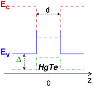
The band structure parameters for HgTe and Hg1-xCdxTe are considered as piecewise constant for each of the layers with an abrupt change at the interfaces, according to the band edge profile in Fig. 4. Using the correct operator ordering in the Hamiltonian [Eqs.(17) and (A.1)], in accordance with the envelope-function approach derived by BurtBurt99 , provides us with an unambiguous determination of the interface boundary conditions. A detailed description of the model, as well as the values of the band structure parameters for HgTe and CdTe, is given in Ref. Novik et al., 2005.
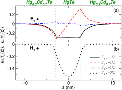
Solving the eigenvalue problem (with an eight-component envelope function vector) we determine the envelope functions and energy levels near for a single QW. In particular, we are interested in the first conduction and valence subbands which for the QW width close to the critical value nm are denoted by E1 and H1 Bernevig et al. (2006). Other subbands are sufficiently apart, so that the system can be described, in a reasonable spectral range Schmidt2009 , by a 4-band effective Hamiltonian Bernevig et al. (2006), with the basis given by the E1 and H1 subband eigenstates at (, , , ). Using the eight-band model described above we calculate these states:
| (19) | |||||
The summation index usually runs over all eight basis states (see Eq.(LABEL:BasisSet)). But for only envelope functions with index given in Eqs.(A.1) have nonzero values. In Fig. 5(a) and (b), we present the envelope functions for E1 and H1 subbands at . Note that and give negligibly small contributions to the total wave function (, ).
A.2 Tunneling matrix in a double quantum well
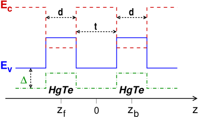
We have proposed an extension of the 4-band effective Hamiltonian Bernevig et al. (2006) for a HgTe/Hg1-xCdxTe QW to a DQW structure. Here, we present a realistic estimation of the parameters in the model equation Eq. 5. We consider a DQW geometry as described in Fig. 6, where we assume a symmetric structure for simplicity. Two HgTe QWs of individual thickness are separated by a barrier of length of Hg1-xCdxTe . When the barrier is sufficiently thin, the electronic states belonging to different layers share a finite overlap. The envelope function of the DQW can be described as a bonding and antibonding combination of the envelope functions of the individual f and b QWs. Each QW has two confined states in the spectral range of interest: the E1 and the H1 subbands. Using the envelope functions for the E1 and the H1 bands discussed in Section A.1 (see Eqs. A.1 and Fig. 5), we can write the tunneling matrix between the states localized on f and b wells as
| (20) | |||||
| (21) |
with
| (22) | |||||
| (23) |
where and are the centers of the f and b QWs, and refers to the E1 and the H1 subbands. is the tunneling matrix previously introduced in our model (in the form of ), while is an additional Rashba-like term, mixing the two Kramer’s block. is the Hamiltonian of the DQW system, which, in the eight-band Kane model basis, has the same form as Eq. (17) and follows the band edge profiles of Fig. 6, with its material-related parameters tuned to their HgTe values in the two intervals and , and to the Hg0.3Cd0.7Te values elsewhere. Note that we neglect the distortion of the band edges due to the electrostatic potential , which in our proposal contributes just a negligible correction with respect to the band offsets between HgTe and Hg1-xCdxTe . We stress that the results of any concrete calculation is obtained for a Cd content in the barriers of . The parameter offers a way to tune the transparency of the barrier. In particular a smaller leads to reduced band edge offsets between the QW and the barrier region (see Fig. 6).
Using the envelope functions of the E1 and H1 subbands, calculated in Section A.1, we calculate the expectation values (integration over ) in Eq.(20) in order to obtain . As expected from the band symmetry (see the related discussion in the note sym, ), has the following structure
| (24) |
with
In Fig. 7(a), we show the dependence of , and on the QW separation for a fixed value of nm-1 (). As expected, both and exponentially decay for increasing length of the tunneling barrier. We note, also, that is very small and for all practical purposes it can be taken as zero. The quantitative difference between and is a direct consequence of the E1 band behaving as an interfacial confined state between HgTe and Hg1-xCdxTe , see Fig. 5. H1 envelope function is, instead, mostly confined in the HgTe layer.
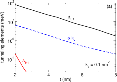
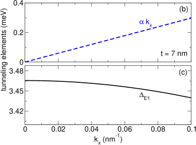
In Fig. 7(b) and (c), we show and as a function of the in-plane wavevector for nm. Parameter shows negligibly weak quadratic corrections, while is strictly a constant. This justifies the treatment of the parameters and as constants in Eq. 5. Table 1 provides the values of and for several values of , for a QW of width nm.
| (nm) | 2 | 3 | 4 | 5 | 6 | 7 |
|---|---|---|---|---|---|---|
| (meV) | 80 | 42 | 22 | 12 | 6 | 3.4 |
| (meV nm) | 66 | 32 | 18 | 10 | 5 | 3 |
Here should be noted that BHZ model is applicable in a finite spectral range Schmidt2009 , this fact restricts the maximum value of the tunneling matrix elements for which the approach we follow is valid. We performed calculations for in a range between nm and nm, observing that the tunneling elements smoothly vary. In particular, for increasing , is slightly reduced (there is a variation of about between values corresponding to QW widths of nm and nm). Parameters and are sensibly increasing with , however in all the explored range .
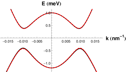
The DQW geometry, breaking the single QW mirror symmetry, generates also Rashba-like tunneling terms described by Eq.(21), which are not included in our model for clarity of the presentation. Our calculation shows that the only significant Rashba-like tunneling element is . However, in our proposal there is an energy potential shift between f and b QWs. This energy detuning between the E1 confined levels in the f and b QWs strongly hinders their coupling by the Rashba-like interaction. In practice, when we include the Rashba-like term in the model, using the realistic tunneling elements we have calculated, it results in a small (compared to the bandgap) tilting of the bulk dispersion curves (see Fig. 8). Due to this, the dispersion curves are characterized by , with only the time reversal symmetry requirement still holding. We note that by turning off adiabatically the Rashba-like term, we can connect the system with Rashba-like interactions to that previously presented in the main body of this work without closing the bandgap. This proves that the topological properties of the system are not affected by the Rashba-like tunneling term in Eq. (21).
| (nm) | 5 | 6 | 7 |
|---|---|---|---|
| (meV) | -3.9 | -1.6 | -0.85 |
In Fig. 8, we show the bulk dispersion curve of a DQW structure employing the tunneling parameters of nm (see Table I), with meV, corresponding to nm, and with a potential shift meV (we note that the electric field employed is about mV/nm, which should be easily achievable in semiconductor heterostructures). Full lines and dashed lines refer to the two Kramer’s blocks. The Rashba-like term in Eq. (21) is included, with meV nm, but its effect, as previously explained, is negligible and consists in a slight tilting of the bands.
A semiconducting gap of meV arises, in agreement with the value obtained with the reduced model Eq 13, using the formula
| (25) |
Table 2 shows the value of the bulk gap for several values of .
For nm, the reduced model (and therefore Eq. 25) is no longer valid due to the large tunneling terms () compared to the individual QW mass term , however the full model [Eq.(3)] still holds (as long as the BHZ model is a reasonable approximation of the band structure).
References
- Laughlin (1981) R. B. Laughlin, Phys. Rev. B 23, 5632 (1981).
- Thouless (1982) D. J. Thouless, M. Kohmoto, M. P. Nightingale and M. den Nijs, Phys. Rev. Lett. 49, 405 (1982).
- Kane and Mele (2005a) C. L. Kane and E. J. Mele, Phys. Rev. Lett. 95, 226801 (2005a).
- Kane and Mele (2005b) C. L. Kane and E. J. Mele, Phys. Rev. Lett. 95, 146802 (2005b).
- Bernevig et al. (2006) B. A. Bernevig, T. L. Hughes and S.-C. Zhang, Science 314, 1757 (2006).
- König et al. (2007) M. König, S. Wiedmann, C. Br ne, A. Roth, H. Buhmann,L. W. Molenkamp, X.-L. Qi and S.-C. Zhang, Science 318, 766 (2007).
- Fu and Kane (2007) L. Fu and C. L. Kane, Phys. Rev. B 76, 045302 (2007).
- Hsieh et al. (2009a) D. Hsieh, D. Qian, L. Wray, Y. Xia, Y. S. Hor, R. J. Cava and M. Z. Hasan, Nature 452, 970 (2009a).
- Zhang et al. (2009) H. Zhang, C.-X. Liu, X.-L. Qi, X. Dai, Z. Fang and S.-C. Zhang, Nat. Phys. 5, 438 (2009).
- Hsieh et al. (2009b) D. Hsieh, Y. Xia, L. Wray, D. Qian, A. Pal, J. H. Dil, J. Osterwalder, F. Meier, G. Bihlmayer, C. L. Kane, Y. S. Hor, R. J. Cava and M. Z. Hasan., Science 323, 919 (2009b).
- Xia et al. (2009) Y. Xia, D. Qian, L. Wray, A. Pal, H. Lin, A. Bansil, D. Grauer, Y. S. Hor, R. J. Cava and M. Z. Hasan, Nat. Phys. 5, 398 (2009).
- Chen et al. (2009) Y. L. Chen, J. G. Analytis, J.-H. Chu, Z. K. Liu, S.-K. Mo, X. L. Qi, H. J. Zhang, D. H. Lu, X. Dai, Z. Fang, S. C. Zhang, I. R. Fisher, Z. Hussain and Z.-X. Shen, Science 325, 178 (2009).
- Moore and Balents (2007) J. E. Moore and L. Balents, Phys. Rev. B 75, 121306 (2007).
- (14) To make the notation more compact, we use four component Pauli matrices .
- (15) The linear off-diagonal coupling is imposed by the rotational symmetry along , in fact the Hamiltonian gives Bernevig et al. (2006), with .
- Novik et al. (2005) E. G. Novik, A. Pfeuffer-Jeschke, T. Jungwirth, V. Latussek, C. R. Becker, G. Landwehr, H. Buhmann, L. W. Molenkamp, Phys. Rev. B 72, 035321 (2005).
- (17) For definiteness, we consider to be real in the remaining of the paper.
- Qi et al. (2006) X.-L. Qi, Y.-S. Wu and S.-C Zhang, Phys. Rev. B 74, 085308 (2006).
- Avron et al. (1988) J. E. Avron, L. Sadun, J. Segert and B. Simon, Phys. Rev. Lett. 61, 1329 (1988).
- Budich and Trauzettel (2011) J. C. Budich and B. Trauzettel (2011), eprint arXiv:1102.3282.
- McCann and Fal’ko (2006) E. McCann and V. I. Fal’ko, Phys. Rev. Lett. 96, 086805 (2006).
- Yang et al. (2008) W. Yang, K. Chang and S.-C. Zhang, Phys. Rev. Lett. 100, 056602 (2008).
- Liu et al. (2008) C. Liu, T. L. Hughes, X.-L. Qi, K. Wang and S.-C. Zhang, Phys. Rev. Lett. 100, 236601 (2008).
- Li and Chang (2009) J. Li and K. Chang, Appl. Phys. Lett. 95, 222110 (2009).
- knez et al. (2011a) I. Knez, R.-R. Du and G. Sullivan, (2011), eprint arXiv:1105.0137.
- knez et al. (2011b) I. Knez, R.-R. Du and G. Sullivan, (2011), eprint arXiv:1106.5819.
- (27) V.A. Zyuzin and G.A. Fiete, Phys. Rev. B 82, 113305 (2010).
- (28) Y. Tanaka and N. Nagaosa, Phys. Rev. Lett. 103, 166403 (2009).
- (29) C.-Y. Hou, E.-A. Kim and C. Chamon, Phys. Rev. Lett. 102, 076602 (2009); A. Ström and H. Johannesson, Phys. Rev. Lett. 102, 096806 (2009); C.-X. Liu, J. C. Budich, P. Recher and B. Trauzettel, Phys. Rev. B 83, 035407 (2011).
- (30) P. San-Jose, E. Prada, E. McCann, and H. Schomerus, Phys. Rev. Lett. 102, 247204 (2009).
- (31) I. Martin, Ya. M. Blanter and A. F. Morpurgo, Phys. Rev. Lett. 100, 036804 (2008).
- (32) M.G. Burt, J. Phys.: Condens. Matter 11, R53 (1999); M.G. Burt, J. Phys.: Condens. Matter 4, 6651 (1992).
- (33) E.O. Kane, J. Phys. Chem. Solids 1, 249 (1957).
- (34) E.O. Kane, in Physics of III-V-Compounds, edited by R.K. Willardson and A.C. Beer (Academic Press, New York, London, 1966), vol. 1 of Semiconductors and Semimetals, p. 75.
- (35) R. Winkler, Spin Orbit Coupling Effects in Two-Dimensional Electron and Hole Systems (Springer, Berlin, Heidelberg, 2003).
- (36) M.J. Schmidt, E.G. Novik, M. Kindermann and B. Trauzettel, Phys. Rev. B 79, 241306 (2009).