11email: wunderlich@physik.uni-siegen.de
Thick-film technology for ultra high vacuum interfaces
of micro-structured traps
Abstract
We adopt thick-film technology to produce ultra high vacuum compatible interfaces for electrical signals. These interfaces permit voltages of hundreds of volts and currents of several amperes and allow for very compact vacuum setups, useful in quantum optics in general, and in particular for quantum information science using miniaturized traps for ions Kielpinski2002 or neutral atoms Schmiedmayer2000 ; Treutlein2006 ; Schmiedmayer2006 . Such printed circuits can also be useful as pure in-vacuum devices. We demonstrate a specific interface, which provides eleven current feedthroughs, more than 70 dc feedthroughs and a feedthrough for radio frequencies. We achieve a pressure in the low mbar range and demonstrate the full functionality of the interface by trapping chains of cold ytterbium ions, which requires the presence of all of the above mentioned signals. In order to supply precise time-dependent voltages to the ion trap, a versatile multi-channel device has been developed.
1 Introduction
Many experiments in atomic and molecular physics are conducted under ultra high vacuum (UHV) conditions to obtain low collision rates with background gas. At the same time, many of these experiments, especially those related to quantum information science require versatile and detailed control Treutlein2006 ; Schmiedmayer2006 ; Rowe2002 ; Stick2006 ; Schulz2008 ; Harlander2011 ; Pearson2006 ; Allcock2010 ; Moehring2011 ; McLoughlin2011 ; Brownnutt2006 . For a recent review of micro-structured ion traps, see Hughes2011 . Unless control is applied using optical fields only Bakr2010 ; Weitenberg2011 , control is usually required in terms of a large number of control voltages Kielpinski2002 ; Rowe2002 ; Stick2006 ; Schulz2008 ; Harlander2011 ; Pearson2006 ; Allcock2010 ; Moehring2011 ; McLoughlin2011 ; Brownnutt2006 or currents Schmiedmayer2000 ; Treutlein2006 , and rf or microwave fields Schmiedmayer2006 ; Boehi2010 ; Karin2011 .
Scaling down such experiments is often desirable, either to improve or simplify trapping, to increase the level of detail on the control of the trapping potential or to make them interesting and competitive for industrial applications. In this case commercially available interfaces impose a serious limit for miniaturization. As a solution, we introduce thick-film technology as a method to produce custom made vacuum interfaces for a large number of signals (as dc and rf voltages and currents) with a small footprint and show that by sealing such parts against simple custom made vacuum components UHV pressure can be attained.

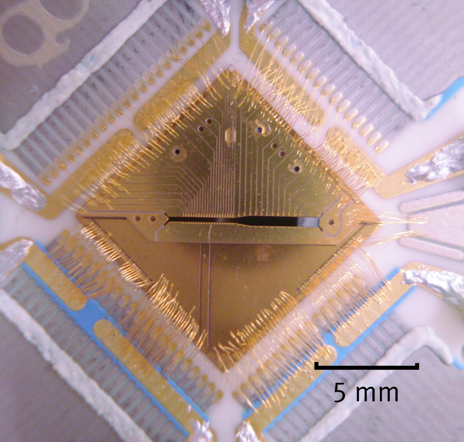
In the remainder of this article, we discuss thick-film technology and its applicability to UHV setups and present the design and describe the manufacturing steps of a specific interface. This interface is used to operate a micro-structured segmented linear ion trap for quantum information science experiments (see figure 1). This trap was designed to trap and laser cool tens of ions in a locally tunable axial potential, and it allows the application of a switchable magnetic field gradient to implement MAgnetic Gradient Induced Coupling (MAGIC) Mintert2001 ; Mintert2001E ; Wunderlich2002 ; Wunderlich2003 ; Ospelkaus2008 . MAGIC provides coupling between internal and motional states and establishes coupling of all spins, mediated by the ions common vibrational motion. MAGIC recently received attention, as it allows to manipulate quantum information with rf Johanning2009b and microwave fields and allows for fast laserless conditional gates Ospelkaus2011 . Furthermore microwave gates were demonstrated with high fidelity Brown2011 , robust states using microwave dressing fields were implemented Timoney2011 , as well as gates which are largely insensitive to detuning and amplitude errors Timoney2008 , the entanglement of non-neighboring ions was shown Khromova2011 , and it has been discussed as a promising approach to implement quantum simulations Johanning2009 ; Welzel2011 .
2 Micro-structured ion trap
Here, we describe the operation of a micro-structured segmented linear ion trap. Such traps allow the tuning of trapping parameters globally and locally. They thus facilitate the splitting and merging of ion strings to implement scalable quantum computing based on simultaneous operations on only two ions Kielpinski2002 , as well as the tailoring of interaction Hamiltonians McHugh2005 ; Wunderlich_H2009 . Providing this amount and detail of control, such traps require a large number of electrical signals. Among these are rf signals with amplitudes of hundreds of volts to achieve trapping of ions, a large number of dc voltages (here, up to 10 volts) to shape the axial trapping potentials, and currents up to a few amperes for atom ovens and (in case of employing MAGIC) for the creation of magnetic fields and gradients.
Our trap is based on a segmented 3-d linear trap design developed in the group of F. Schmidt-Kaler Schulz2008 ; Schulz2006 , other three dimensional microstructured traps are described, for instance, in Rowe2002 ; Stick2006 ; Harlander2011 ; Brownnutt2006 . Ions are trapped in the slit of a linear Paul trap composed of three laser-machined layers made of alumina (Al2O3). The outer gold-coated layers (in the following called top and bottom layer) feature electrically separated areas which form a pattern of dc and rf electrodes that provides the entire trapping functionality. The trap offers a wide loading region with nine segments, a narrow region for tight confinement with nineteen segments and a three segment taper to connect the two regions (see figure 1).
The photo in figure 1 shows the mounted microtrap. The trapping potential is generated within the slit in the middle of the quadratic trap chip structure. Inside the loading region the slit is 500 µm wide and narrows down to 250 µm in the narrower trapping region. The total length of the slit is 7.4 mm, the edge length of the whole trap chip is 11 mm. The micro-structured design of the trap allows for trapping ions in different trap regions, moving them along the slit and applying magnetic gradients to the trapped ions.
The middle layer (stacked between the outer layers) was specifically developed to provide an adjustable magnetic field gradient. This layer is made of gold coated, electroplated alumina. We use the conductivity of this layer to apply a current for generating magnetic fields and gradients in the proximity of the trapped ions, in order to address and couple trapped ions in the MAGIC-scheme. To boost the coupling induced by the magnetic field gradient, it is desirable to attain as large gradients as possible and this design was optimized for low dissipated heat per gradient, as the current limit through the coil is given by the damage threshold of the coil structure and its connections. In a preliminary test, we found that several amperes could be applied without any damage. As this preliminary test was done on a test structure with high ohmic resistances and no cooling, we expect to be able to apply more than 10 A of current on the setup. To avoid the wire bonds being a bottleneck, the current is distributed over many bonding wires when feeding it to the chip. The large number of additional wire bonds required cropping of the top layer, to provide sufficient space for large bond pads on the middle layer (see figure 1). Laser cut Polyimid foils inserted between all trap layers isolate the entirely gold coated middle layer from the outer trap layers electrically. Details on the design and functionality of the magnetic field generating elements will be published elsewhere. In order to provide all necessary connections, a compact solution was developed and is described in what follows.
3 Microtrap Chip Carrier
3.1 Thick-film technology
We adopt thick-film technology to design a compact carrier for micro-structured traps which simultaneously acts as a vacuum interface. Thick-film technology is a well-known technique for the fabrication of electronic circuits Harper1974 ; Gupta2005 . With a screen printing process, wire structures are printed onto ceramics or other suitable insulating materials. After the printing process, e.g. on alumina, the printed conducting paste has to be fired at 850 ∘C. Small glass particles inside the conducting paste fuse, and the printed structures reliably cling to the ceramic surface. After the first printing has been fired, more complex structures and circuits can be generated by successively adding more layers on top of an already fixed structure.
The paste used in the process is not limited to conducting paste (which can contain e.g. silver and palladium, or gold), but also isolating pastes as well as resistor pastes and pastes to create specific dielectric layers (e. g. to create printed capacitors) are available. Thick-film technology can be used to produce wire structures with a minimum width of less than 0.1 mm. Using a laser to trim the printed circuits, even smaller structures can be fabricated. With the same technique, thick-film resistors can be adjusted to accuracies of better than 0.1 %. The wire bonding technique, conducting glue and even common soldering can be used to connect the printed structures to certain setups.
We found that thick-film printed ceramics can be used in UHV environments (see Sec. 4). For our purpose, alumina is advantageous as a base material, because the heat conductivity of this ceramic is comparatively high (about 25 W/(Km)) and allows to remove any thermal intake from ohmic heating.
3.2 Design and implementation
In order to conduct experiments with the microtrap, a radio frequency voltage, 70 dc-voltages, and currents of several amperes have to be applied to the trap. Furthermore, heat generated from ohmic losses needs to be removed. As ion trapping can only be performed in an UHV environment, all signals have to be fed through vacuum interfaces. In order to reduce noise and rf crosstalk on dc electrodes, low pass filters connected to every dc electrode should be located close to the trap (in our design we achieve less than 10 cm).
All these requirements were implemented with a single thick-film printed ceramic block forming the microtrap chip carrier. This chip carrier consists of a 15 mm thick block of alumina with outer dimensions of 65 mm 75 mm.
The design of the thick-film printed structure for the upper side of the chip carrier is illustrated in figure 2. From left to right, the sequence of the printing process is indicated to allow a detailed view of the complex structure. Figure 2a shows the blueprint of silver-palladium wires connecting to the 70 dc electrodes, and the tapered rf electrode’s connection with two shielding wires printed next to it. To fabricate low pass filters close to the microtrap, the next two printing steps provide a capacitance overlaying all wires, which connects to all dc electrodes. In order to form this capacitor, blue isolation paste was printed upon the wire structure in a first step (see figure 2b). Figure 2c shows the structure of the conducting capacitance layer. In the last two printing steps (shown in figure 2d), a ring of blue isolation paste for the vacuum interface, and golden pads for wire bonding were fabricated. The isolation layer of the capacitor was printed twice in order to prevent shortcuts. For the ring, three isolating layers provide a thickness of at least 20 µm to apply polishing (see section 4). Although we gained positive experience with resistive pastes, we keep all resistors for filtering outside vacuum on nearby exchangable filter boards to keep them fully flexible (see section 6). The thickness of the chip carrier is 15 mm and thus provides good mechanical stability and allows to add stud holes for heat pipes to cool the whole carrier from the air side.
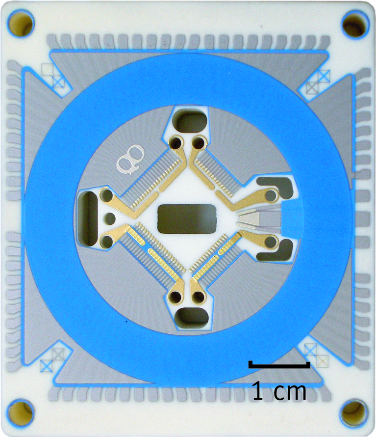
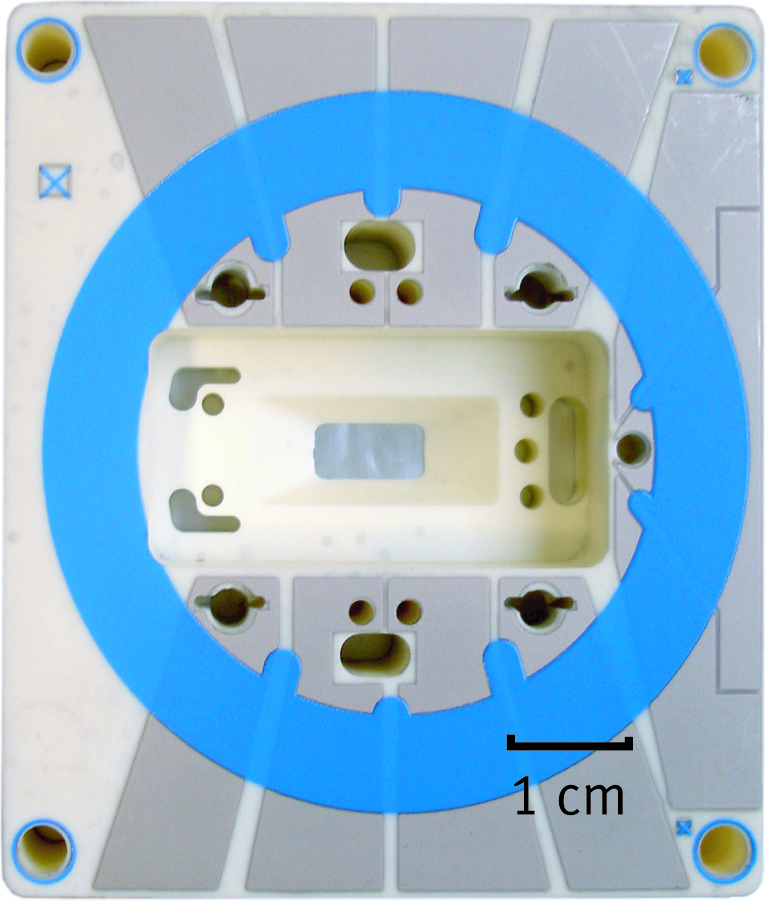
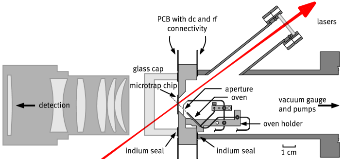
The microtrap chip carrier, completely fabricated, is displayed in figure 3a and 3b. Figure 3a shows the top view of the carrier, designed as illustrated in the blueprints of figure 2. This final thick-film printed design provides a capacitance of (44 3) pF for each dc connecting wire. Several holes in the ceramic block (indicated in red in figure 2a) are pumping holes to provide good pumping through the carrier. The rectangular hole in the middle of the carrier (indicated in blue in figure 2a) is located where the trap is mounted. All other holes are feedthroughs for screws in order to connect electrically the upper and the lower side of the chip carrier and to fix the atomic ovens (see overview in figure 4). Figure 3b shows the bottom view of the chip carrier, which is used to provide high current supplies for the atomic ovens and the coil structure providing the magnetic gradient. Furthermore, it contains a thick-film printed isolation ring similar to the one on the top side of the carrier.
The trap is glued to the carrier and electrically connected with wire bonds (see figure 1). A reliable connection is ensured by connecting each dc electrode with two bonding wires.
4 Vacuum
4.1 Indium seals
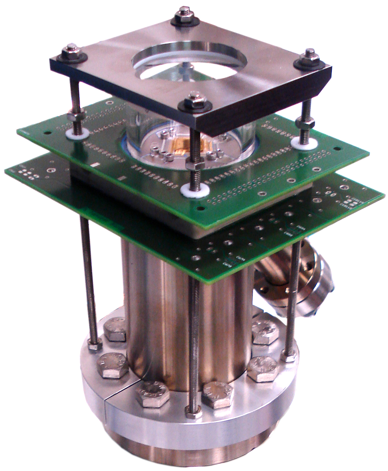
To achieve a pressure in the UHV range required for this experiment we found that placing rings of indium between polished surfaces of the vacuum components offers a reliable sealing method. The essential vacuum system can be seen in figure 4. The chip carrier is placed between a glass cap with an interferometric quality window towards the left, which ensures good optical access and a steel chamber which connects to standard UHV components (pumps and a gauge) with ISO-CF flanges to the right. The contact surfaces of the glass cap and the steel chamber are polished, but no optical surface quality is required. The counterparts of these surfaces on the chip carrier (the rings of isolating paste, visible as blue rings in figure 3) were polished as well.
Indium wires with a diameter of 0.5 mm were placed between the polished surfaces and the stack was compressed with four M4 screws applying a torque of 0.5 Nm (see setup shown in figure 6). Indium will create a compression seal due to its low elasticity modulus (10.5 GPa Werkstoffe ). We proved the tightness of the indium seals with helium leak tests using a quadrupole mass spectrometer and found the signal to be dominated by the slow rise due to diffusion through the chamber walls. A diminutive amount of vacuum grease is used on all surfaces to be able to separate the pieces without excessive application of force because indium is sticky and would otherwise be difficult to remove when reopening the chamber.
4.2 Vacuum system
The vacuum parts visible in figure 4 connect to further standard stainless steel UHV components. The main components are an ion getter pump, a titanium sublimation pump and an ion gauge, all connected via standard CF40 parts.
All steel parts were baked on air at approximately 300 ∘C for three days, to reduce the achievable vacuum pressure Park2008 . In a second step, we connected the setup shown in figure 6 to a turbo molecular pump and applied a second clean bake at approximately 120 ∘C (compatible with all components built in and below the melting temperature of indium at 156.4 ∘C Werkstoffe ) for three days to remove any excess amount of vacuum grease from the system. After this cleaning bake, the ion getter pump, the titanium sublimation pump and the ion gauge were assembled and the final bake at approximately 120 ∘C was applied for four days.
After four months of daily ion trapping the pressure is in the low mbar range. We can observe 172Yb-ions over a time span of approximately seven hours. This was estimated from trapping of larger samples and observing the lifetime of the complete chain.
5 Electrical Interconnect
All control voltages and currents are supplied to the microtrap carrier via two double-layer printed circuit boards (PCB) which provide quick and convenient multi-pin connectors to connect to any signal source (see figure 6). The high thermal conductivity and the large mass of the chip carrier (compared to the PCBs) exclude the use of conventional soldering techniques (soldering and reflow soldering). As an alternative, conductive epoxy is used to connect the chip carrier to the PCBs.
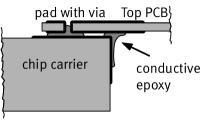
The upper PCB (in the following called top-PCB) is connected to the chip carrier as indicated in figure 5. The large number of pads on this board requires small sizes and increases the risk of accidental shortcuts from spreading glue. To resolve this problem, each pad on the top-PCB has a 0.95 mm-hole, which can be used to check the alignment (to the corresponding pad on the chip carrier) and to insert the correct amount of glue using a syringe. To allow for controlled spreading of the glue we found that a gap of approximately 0.3 mm between chip carrier and PCB is essential. An additional drop of epoxy at the side of the carrier (see figure 5) increases the mechanical strength and conductivity of the connection. This technique ensures fault free connectivity for all connections of top-PCB by providing the possibility to check and repair (if required) any bad contact or short cut between neighbouring pads before proceeding to curing. The resistance between bond pads and the top-PCB after curing was found to be below 15 Ω for all connections.
All dc electrodes require currents only in the mA-regime, whereas higher currents are necessary to drive our atom ovens (up to 2.5 A, see section 8) or to generate magnetic fields gradients. All higher currents are provided through the lower board (called bottom-PCB). We achieved substantially lower resistivity compared to the upper side using tapered wires on the chip carrier and large pad areas (65 mm2 – 121 mm2) for large cross sections of the conductive epoxy connections, accompanied by thick, short and wide traces on the bottom-PCB. On the other hand, scaling up the width per connection results in a much lower number of connections on this board (11 total). The resistance between chip carrier and the bottom-PCB after curing was found to be below 90 mΩ for all connections.
6 Trapping potentials
The rf potential required for the Paul trap is provided to the microtrap using a frequency generator which can be amplified before feeding the signal to a helical resonator (for design details, see Weisgerber2003 ; Macalpine1959 ; Vizmuller1995 ; Zverev1967 ). Apart from designing the trap for low capacitance, we tried to keep the load capacitance small (about 30 pF) by connecting the helix to the microtrap with a short (5 cm) co-axial cable and short connections on the top-PCB and the chip carrier. The rf feedthrough introduces a capacitance of about 1-3 pF. The -factor of the helix with connected microtrap system exceeds 500, which is comparable to the -factor obtained with a conventionally connected trap.
All dc potentials for the segmented electrodes are provided by computer-controlled DAC channels via a routing device which allows each signal to be connected to any number or pattern of electrodes.
We also developed an Electric Field Generator (EFG) EFG-patent which provides versatile dc potentials required for a fast and detailed control of the axial trapping potential, e.g. for shuttling of ions between trapping and processing zones. The EFG in its present version provides 20 channels and is planned to be extended to 100 channels in the future. Potentials up to 15 V can be controlled with an update rate up to 20 MHz, a precision of approximately 1 mV, and a noise level below 0.5 mV. The device allows to program, store and quickly recall up to 16 different output waveform patterns for each channel. High bandwidth and update rates, as possible with this device, are interesting for ultra-fast transport between trap segments Schulz2006 , or, provided the update rate substantially exceeds the trap drive frequency, even to compensate micromotion where this is impossible with dc (e.g. due to rf field components along the trap axis). For quantum simulations in surface traps, such a device could provide arbitrary superpositions of dc and rf on each pixel electrode, giving full freedom for the lattice geometry of the trapped ions. Details on the EFG will be published elsewhere.
It is desirable to remove stray fields and rf crosstalk on all dc electrodes to obtain clean trapping potentials. We achieve this using the printed capacitance on the chip carrier (explained in section 3, and shown in figure 2), and an additional low-pass filter for each dc electrode. Each of these filters is similar to a -filter with two capacitors (1 µF each) but with a resistor (15 kΩ) instead of an inductor. The filters are implemented on an exchangable 4-layer PCB. This filter is plugged into the Top-PCB from the air side, and can easily be replaced, if desired, by another filter-PCB with a different characteristics such as a notch filter.
7 Lasers and detection
The fine structure of ytterbium requires two lasers for laser cooling Balzer2006 : one laser at 369 nm drives the 2S1/2 -2P1/2 -transition for cooling and detection, a second laser at 935 nm drives the 2D3/2 - -transition to avoid optical pumping into the metastable 2D3/2 state. Another laser at 638 nm is useful to pump back atoms from the 2F7/2 state which is occasionally populated by collisions. A fourth laser at 399 nm drives the 1S0 -1P1 -transition in neutral ytterbium and is used for isotope selective photoionization Johanning2011 . A feature of ytterbium is the availability of all these wavelengths from laser diodes. All lasers are set up as external cavity diode lasers in Littrow configuration and locked to pressure sealed temperature stabilized Fabry-Perot cavities by a side of fringe lock. The 369 nm laser diode needs to be cooled down to ∘C to reduce the free-running wavelength Kielpinski2006 by 1.9 nm and requires an air tight housing to avoid condensation of water on the cold surface. The lasers are coupled into single mode fibres and are combined with dichroic mirrors into a single beam which is focused by a beam shaping telescope into the trap region. The fibre collimators are adjusted to compensate chromatic aberrations of the focussing telescope. The beam is directed with two mirrors through the trap slit. One of these mirrors is a piezo motor controlled mount with an alignment precision of sub micrometer and it determines the position where the laser beams cross the trap.
The fluorescent light from the trapped ions is collimated by a custom made lens system Schneider2007 (see also figure 4), optimized for a large numerical aperture of 0.4, whilst maintaining a diffraction limited spot over a field of view of 500 µm. The collimated resonance fluorescence can be directed either to a photo multiplier tube (PMT) or to an EMCCD Camera. Simultaneous observation of resonance fluorescence from ions on the camera and from neutral atoms on the PMT is also possible using a dichroic mirror. We use a single-band pass filter with a transmission peak at 370 nm and a width (FWHM) of 6 nm in front of the camera to detect fluorescence light from the ion. Additional adjustable apertures are placed in auxiliary focal planes to further discriminate against unavoidable stray-light from the trap electrodes at the cooling wavelength of 369 nm.
8 Loading and trapping
To start trapping ions, all lasers are locked to temperature stabilized cavities and set to the correct wavelength McLoughlin2011 . The reproducibility of our home-built scanning Michelson lambdameter and all lasers is on the order of a few tens of Megahertz and sufficient to ensure successful loading, once the correct wavelengths are set.
We create collimated beams of neutral ytterbium atoms by ohmic heating of a small sample of granular ytterbium in a miniature tube-shaped steel oven (for design, modelling and operation, see Johanning2011 ; Eiteneuer2009 ). Two identical ovens, mounted to the oven holder (see figure 4) approximately aligned in a plane normal to the laser beam, are filled with isotopically enriched samples of 171Yb and 172Yb, respectively. Deposition of ytterbium atoms on electrodes in the regions relevant for high fidelity experiments is avoided by skimming the atomic beams by apertures. Further reduction of neutral atom deposition on trap electrodes is accomplished by aligning the atomic beam such that it intersects the trap axis approximately in the middle of the wide loading region. At this position, due to the separation of approximately 500 µm from the taper region, the influence of unwanted axial rf field components is sufficiently screened to be negligible.
Atomic ions are produced using a two-step photo-ionization process, with a resonant first step (see Johanning2011 for details). When there is no filter in the detection channel discriminating light at 399 nm, the effectiveness of photoionization can be deduced from the neutral atom fluorescence. Visible resonance fluorescence from neutral atoms can serve as a first frequency reference and calibration of the lambdameter with an atomic standard. It also indicates excessive neutral atom flux, which is detrimental for our vacuum and causes undesirable coating of the electrodes with ytterbium.
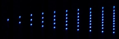
We usually set the oven current, such that the ion loading rate is small enough (less than one per second) to load ions one by one. The first ion is loaded during the warm-up of the oven after approximately two minutes, starting from a cold oven. The loading rate is then slowly accelerated and longer chains can be loaded within a few minutes (see figure 7). Applying an rf power of 125 mW results in a radial trapping frequency of 888 kHz, corresponding to an rf amplitude of approximately 200 V and a stability parameter of . The rf drive frequency is 7.7 MHz. The pressure rises during the loading process up to the mid-10-11 mbar range.
9 Outlook
We showed that thick-film technology allows to generate customized vacuum feedthroughs for electrical signals. These feedthroughs were shown to be suitable for dc and rf signals with voltages up to a few hundreds of volts and for currents up to a few amperes. Gold pastes are available with up to eight times higher conductivity and should allow for even smaller current interfaces or larger currents. Moreover, it should be possible, using a proper design, to extend the frequency range into the microwave regime. Thick-film interfaces allow for compact designs with very good access for lasers, detection, rf- and microwave-fields. Such interfaces are useful in general atomic and molecular physics, especially when working with micro-structured components, such as traps for neutral atoms or ions. The vacuum compatibility was found to be satisfying and matches usual requirements in atomic and molecular physics, as we regularly attain pressures in the low mbar range.
We also used similar multi-layered thick-film based chip carriers as pure in-vacuum devices as they allow for complex structures, as, for example, solder free filter boards in the immediate vicinity of the trap to passively remove noise from dc electrodes. For this purpose not only conductive and isolating pastes are available (which alone are sufficient to create capacitors) but also resistive pastes for printed resistors and dedicated dielectric pastes to create compact capacitors. The properties of such circuits can be fine-tuned precisely by changing the area of printed structures using laser trimming Gupta2005 . Even more applications are possible by thick-film hybrid technology, which combines thick-film technology with conventional (glued or soldered) SMD elements.
The scope of the experiment described in this article is to utilize switchable and tunable magnetic field gradients to use MAGIC. Together with the flexibility of the axial trapping potential McHugh2005 ; Wunderlich_H2009 ; Schulz2006 this should allow for interesting experiments rooted in quantum information science and to generate tailored Hamiltonians for quantum simulations.
The strong magnetic field gradient extends over a few hundreds of micrometers and ions need to be shuttled into the experiment region (located approximately in the middle of the narrow trap slit, see figure 1) to experience its effect. Thereupon MAGIC can be utilized using radio frequency fields operating on Zeeman levels of the 2S1/2 ground state or, for an easier shelving on Zeeman levels of the 2D3/2 manifold Johanning2009b . Another possibility is to use the isotope 171Yb+which provides a nuclear spin of and is thus more difficult to laser cool, since the hyperfine structure requires additional repumping fields.
MAGIC provides the potential to perform quantum information science experiments using Doppler cooled ions, removing the obstacle (or nuisance) of ground state cooling, associated with many implementations of ion trap based quantum logic. But on the other hand, as the gradient couples internal and motional states, it allows for sideband cooling using microwaves, simultaneous cooling of many vibrational modes Wunderlich2005 and allows to improve laser cooling altogether Albrecht2011 .
Appendix A: Technical Details
The microtrap chip carrier consists of a 15 mm thick block of alumina with outer dimensions of 65 mm 75 mm. It was milled by MicroCeram GmbH Meissen. The thick film printing of the block was carried out by the Hybrid Laboratory of the University of Siegen.
For the thick film prints, isolating paste DuPont 5704, gold paste DuPont 5722L and silver-palladium paste DuPont LF 121 were used. As the thickness of the alumina block is about 15 times higher than typical thick-film printed ceramics, the firing process had to be adjusted. Instead of a standard 50 K/min slope a maximum velocity of 20 K/min was implemented. The maximum temperature of 850 ∘C was held for 20 min instead the typical 10 min. The whole cycle lasted 120 min. The typical height of printed thick film structures is 7-11 µm.
For the polishing procedure,
polishing heads with a ring shaped end face
were built of aluminium to be able to just polish the ring shaped areas of
isolation paste described above. The polishing heads were equipped
with special cloth for the polishing pastes, Winter-Diamant
polishing cloth D0,7-D0,25, of Saint Gobain Diamantwerkzeuge.
The polishing heads were then mounted on a drilling machine, operating at 480 rounds per
minute, and the isolation rings were polished for about 10 s with diamond-pastes
Winter-Diaplast N D 0,7 with a particle size of 0.7 µm or N D 0,25 with a particle size of
unit[0,25]µm with small force.
After this, the surface was checked under a light cut microscope. Typically after two or three polishing cycles, the surface no longer showed the screen printing structure and was smoothly polished. On such a surface, the indium seals were always tight.
For the sealing, indium wire with a diameter of 0.5 mm and a pureness of 99.99 % is used. Before putting the indium wire onto the surfaces, a diminutive amount of vacuum grease Pfeiffer Vacuum BN845805-T is applied. After that, the indium was formed to a ring of a diameter according to the diameter of the isolating rings. The endings of the indium wire were crossed over each other, before putting the indium ring onto the surface.
The pastes used in thick-film technology are hardening slowly during storage and processing and the viscosity rises perceptibly. We believe this is the reason that in some of our prints, we found small leaks along a few radial wires when leak testing with helium, presumably caused by micro channels. As a precaution, we applied a narrow layer of leak sealing Torr Seal Vacuum Epoxy, Varian, along the edges of the isolating pastes to seal all potential channels and found that this procedure results in helium tight interfaces reliably. We expect this sealing step to be unnecessary, when using fresh paste with low viscosity for thick-film printing.
Detailed design guidelines specific for the thick-film-printing facilities at Siegen are available upon request from the authors.
Acknowledgments
We gratefully acknowledge our electrical and mechanical work shops and especially D. Gebauer, who accomplished the thick-film printing for our chip carrier. We thank Andrés F. Varón for fruitful discussions. We acknowledge financial support by the European Union (STREP Microtrap and PICC), by the Deutsche Forschungsgemeinschaft and by secunet AG.
References
- (1) D. Kielpinski, C. Monroe, and D. J. Wineland, Nature 417, 709 (2002).
- (2) R. Folman, P. Krüger, D. Cassettari, B. Hessmo, T. Maier, and J. Schmiedmayer, Phys. Rev. Lett. 84, 4749 (2000).
- (3) P. Treutlein, T. Steinmetz, Y. Colombe, B. Lev, P. Hommelhoff, J. Reichel, M. Greiner, O. Mandel, A. Widera, T. Rom, et al., Fortschr. Phys. 54, 702 (2006).
- (4) S. Hofferberth, I. Lesanovsky, B. Fischer, J. Verdu, and J. Schmiedmayer, Nat. Phys. 2, 710 (2006).
- (5) M. A. Rowe, A. Ben-Kish, B. Demarco, D. Leibfried, V. Meyer, J. Beall, J. Britton, J. Hughes, W. M. Itano, B. Jelenkovic, et al., Quant. Inf. Comp. 2, 257 (2002).
- (6) D. Stick, W. K. Hensinger, S. Olmschenk, M. J. Madsen, K. Schwab, and C. Monroe, Nat. Phys. 2, 36 (2006).
- (7) S. Schulz, U. Poschinger, F. Ziesel, and F. Schmidt-Kaler, New J. Phys. 10 (2008).
- (8) M. Harlander, R. Lechner, M. Brownnutt, R. Blatt, and W. Hänsel, Nature 471, 200 (2011).
- (9) C. E. Pearson, D. R. Leibrandt, W. S. Bakr, W. J. Mallard, K. R. Brown, and I. L. Chuang, Phys. Rev. A 73, 032307 (2006).
- (10) D. T. C. Allcock, J. A. Sherman, D. N. Stacey, A. H. Burrell, M. J. Curtis, G. Imreh, N. M. Linke, D. J. Szwer, S. C. Webster, A. M. Steane, et al., New J. Phys. 12, 053026 (2010).
- (11) D. L. Moehring, C. Highstrete, D. Stick, K. M. Fortier, R. Haltli, C. Tigges, and M. G. Blain, New J. Phys. 13, 075018 (2011).
- (12) J. J. McLoughlin, A. H. Nizamani, J. D. Siverns, R. C. Sterling, M. D. Hughes, B. Lekitsch, B. Stein, S. Weidt, and W. K. Hensinger, Phys. Rev. A 83, 013406 (2011).
- (13) M. Brownnutt, G. Wilpers, P. Gill, R. C. Thompson, and A. G. Sinclair, New J. Phys. 8, 232 (2006).
- (14) M. D. Hughes, B. Lekitsch, J. A. Broersma, and W. K. Hensinger, Cont. Phys. 52 (2011).
- (15) W. S. Bakr, A. Peng, M. E. Tai, R. Ma, J. Simon, J. I. Gillen, S. Fölling, L. Pollet, and M. Greiner, Science 329, 547 (2010).
- (16) C. Weitenberg, M. Endres, J. F. Sherson, M. Cheneau, P. Schauss, T. Fukuhara, I. Bloch, and S. Kuhr, Nature 471, 319 (2011).
- (17) P. Böhi, M. F. Riedel, T. W. Hänsch, and P. Treutlein, Appl. Phys. Lett. 97 (2010).
- (18) T. Karin, I. Le Bras, A. Kehlberger, K. Singer, N. Daniilidis, and H. Häffner, Appl. Phys. B 106, 117 (2011).
- (19) S. Schulz, U. Poschinger, K. Singer, and F. Schmidt-Kaler, Fortschr. Phys. 54, 648 (2006).
- (20) F. Mintert and C. Wunderlich, Phys. Rev. Lett. 87, 257904 (2001).
- (21) F. Mintert and C. Wunderlich, Phys. Rev. Lett. 91, 029902 (2003).
- (22) C. Wunderlich, in Laser Physics at the Limits (Springer, 2002), pp. 261–271.
- (23) C. Wunderlich and C. Balzer, Advances in Atomic, Molecular, and Optical Physics 49, 293 (2003).
- (24) C. Ospelkaus, C. E. Langer, J. M. Amini, K. R. Brown, D. Leibfried, and D. J. Wineland, Phys. Rev. Lett. 101, 090502 (2008).
- (25) M. Johanning, A. Braun, N. Timoney, V. Elman, W. Neuhauser, and C. Wunderlich, Phys. Rev. Lett. 102, 073004 (2009).
- (26) C. Ospelkaus, U. Warring, Y. Colombe, K. R. Brown, J. M. Amini, D. Leibfried, and D. J. Wineland, Nature 476, 181 (2011).
- (27) K. R. Brown, A. C. Wilson, Y. Colombe, C. Ospelkaus, A. M. Meier, E. Knill, D. Leibfried, and D. J. Wineland, Phys. Rev. A 84, 030303 (2011).
- (28) N. Timoney, I. Baumgart, M. Johanning, A. F. Varón, M. B. Plenio, A. Retzker, and C. Wunderlich, Nature 476, 185 (2011).
- (29) N. Timoney, V. Elman, S. Glaser, C. Weiss, M. Johanning, W. Neuhauser, and C. Wunderlich, Phys. Rev. A 77, 052334 (2008).
- (30) A. Khromova, C. Piltz, B. Scharfenberger, T. F. Gloger, M. Johanning, A. F. Varón, and C. Wunderlich, arXiv:1112.5302v1 [quant-ph] (2011).
- (31) M. Johanning, A. F. Varón, and C. Wunderlich, J. Phys. B 42, 154009 (2009).
- (32) J. Welzel, A. Bautista-Salvador, C. Abarbanel, V. Wineman-Fisher, C. Wunderlich, R. Folman, and F. Schmidt-Kaler, arXiv:1102.3645v2 (2011).
- (33) D. Mc Hugh and J. Twamley, Phys. Rev. A 71, 012315 (2005).
- (34) H. Wunderlich, C. Wunderlich, K. Singer, and F. Schmidt-Kaler, Phys. Rev. A 79, 052324 (2009).
- (35) C. A. Harper, Handbook of Thick Film Hybrid Microelectronics (McGraw-Hill Book Company, 1974).
- (36) T. K. Gupta, Handbook of Thick- and Thin-Film Hybrid Microelectronics (John Wiley & Sons, Inc., 2005).
- (37) M. Merkel and K.-H. Thomas, Taschenbuch der Werkstoffe (Carl Hanser, 2008), 7th ed.
- (38) C. D. Park, S. M. Chung, X. H. Liu, and Y. L. Li, Journal of Vacuum Science & Technology A 26, 1166 (2008).
- (39) I. Weisgerber, Aufbau eines Magnetfeldsystems, eines Helixresonators und eines optischen Strahlenganges, Dipl., University of Hamburg (Hamburg, 2003).
- (40) W. W. Macalpine and R. O. Schildknecht, Proc. IRE 47, 2099 (1959).
- (41) P. Vizmuller, RF Design Guide: Systems, Circuits, and Equations (Artech House, Inc., London, 1995).
- (42) A. I. Zverev, Handbook of Filter Synthesis (John Wiley & Sons, Inc., New York, 1967).
- (43) Electric field generator, german patent application de 10 2011 001 399.7, filed on march 18, 2011.
- (44) C. Balzer, A. Braun, T. Hannemann, C. Paape, M. Ettler, W. Neuhauser, and C. Wunderlich, Phys. Rev. A 73, 041407 (2006).
- (45) M. Johanning, A. Braun, D. Eiteneuer, C. Paape, C. Balzer, W. Neuhauser, and C. Wunderlich, Appl. Phys. B 103, 327 (2011).
- (46) D. Kielpinski, M. Cetina, J. A. Cox, and F. X. Kärtner, Opt. Lett. 31, 757 (2006).
- (47) C. Schneider, Entwicklung eines Objektivs hoher numerischer Apertur zum Nachweis der Resonanzfluoreszenz einzelner gespeicherter Ionen, M.sc., University of Siegen (Siegen, 2007).
- (48) D. Eiteneuer, Bau und Charakterisierung einer Ytterbium-Quelle für mikrostruktierte Ionenfallen, M.sc., University of Siegen (Siegen, 2009).
- (49) C. Wunderlich, G. Morigi, and D. Reiß, Phys. Rev. A 72, 023421 (2005).
- (50) A. Albrecht, A. Retzker, C. Wunderlich, and M. B. Plenio, New J. Phys. 13 (2011).