Spatial Mapping and Manipulation of two tunnel coupled Quantum Dots
Abstract
The metallic tip of a scanning force microscope operated at is used to locally induce a potential in an fully controllable double quantum dot defined via local anodic oxidation in a GaAs/AlGaAs heterostructure. Using scanning gate techniques we record spatial images of the current through the sample for different numbers of electrons on the quantum dots, i.e. for different quantum states. Owing to the spatial resolution of current maps, we are able to determine the spatial position of the individual quantum dots, and investigate their apparent relative shifts due to the voltage applied to a single gate.
pacs:
XXXI Introduction
Most quantities measured in pure transport experiments, such as the current through a nanostructure, remain macroscopic and contain little spatial information. To justify assumptions about the potentially spatially non-uniform current flow in nanostructures it is highly useful to employ a probing technique which offers spatial resolution. Scanning gate microscopy, where a metallic tip is used to capacitively couple to the nanostructure acting as a freely movable gate, is a powerful local probing technique. It has been applied to a broad range of materials from 2DEG-based semiconductors Topinka_Nature_2001 ; Pioda_PRL_2004 ; Steele_PRL_2005 ; Crook_Science_2006 ; Hackens_NaturePhys_2006 over InAs nanowires Bleszynski_PRB_2008 and graphene Bleszynski_condmatt_2009 ; Schnez_Scheissteil_2010 to superconductors huefner_PRB_2009 . While it has been applied to investigate accidentally formed multiple dots Bleszynski_NanoLett_2007 ; Woodside_science_2002 no investigations of controllable, intentionally formed double dots have been reported to date.
Here we show that we can control single electrons on a double quantum dot by moving a metallic tip across the structure. Spatial current maps allow us to gain insight into the topographic position of the charge distribution of the two quantum dots themselves.
II Sample and Setup
The double quantum dot under investigation has been fabricated on an AlGaAs-GaAs heterostructure, which contains a two-dimensional electron gas (2DEG) below the surface. The 2DEG has a density of and a mobility of at . The double quantum dot structure has been predefined by local anodic oxidation Fuhrer_SuperMicro2002 at room temperature. With this technique oxide lines are formed on the surface, below which the 2DEG is locally depleted. Thus the oxide lines electrically separate adjacent 2DEG areas. Figure 1(a) shows a scanning force microscope (SFM) scan of the investigated structure recorded at a temperature of . The oxide lines are seen as bright protrusions. The positions at which the quantum dots are expected to form are marked with two red dots labeled ”dot 1” and ”dot 2”. The double quantum dot is electrically contacted via tunneling barriers to source (S) and drain (D). The tunneling barriers between source and dot 1 as well as between dot 2 and drain can be tuned with the gates marked STG and DTG respectively. The levels inside each dot can be shifted by applying a voltage to the 2DEG-areas marked PG1, PG2, QPCG1 and QPCG2. The central gate (CG) tunes the interdot coupling.
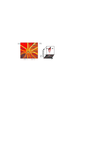
All experiments shown here are performed with a SFM in a 3He cryostat with a an electronic temperature of about . The scanning force sensor consists of an electrochemically etched PtIr tip with an initial radius of about , mounted on a piezoelectric tuning fork. The measurements presented in this work are recorded with a clean single tip. Figure 1(b) schematically shows the tip-induced local electrostatic potential (tip potential) in the sample that can be moved freely in x-y-direction. The coordinates x and y indicate the lateral tip position. The tip-surface distance for all current maps presented here is unless stated otherwise. The tip induced potential is about for . Investigations of the interaction potential between the tip and the sample in previous measurements Pioda_PRL_2004 ; huefner_PRB_2009 have shown that even at zero volt tip voltage there is still a noticeable potential induced in the sample. Moving the tip potential in real space across the double quantum dot shifts the electrochemical potential of quantum states. We record so-called current maps, which show the current through the double dot as a function of the tip position . No current flows between the tip and to the 2DEG.
III Charge stability diagram in real space
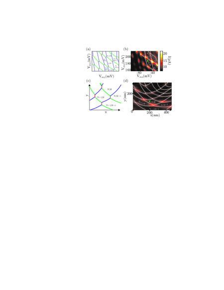
The charge stability diagram of a double quantum dot displays hexagonal patterns as schematically shown in Fig. 2(a). This pattern mainly consists of lines with two different slopes marked in blue and green. Along the green lines, a quantized energy level of dot 1 is in resonance with source and drain electrochemical potentials. Analogously along the blue lines an energy level of dot 2 is in resonance with the electrochemical potential of source and drain. We can attribute a certain number of electrons on each dot to given gate voltage regions as marked by letters in the schematics and in the corresponding measurement in Fig. 2(a,b).
Panel (b) shows the current through the double quantum dot as a function of the voltage applied to PG1 and applied to PG2. The honeycomb pattern characteristic for the charge stability diagram of a double dot can be observed Wiel_RevModPhys_2002 ; Reed_Book_1989 ; Hanson_PvModPhys_2007 . Since the electronic temperature is larger than the mutual charging energy, pairs of triple points form a single current peak. Some pairs of triple points are connected by cotunneling lines of nonzero current. Along such a line, a level of only one quantum dot is aligned with the Fermi energy of source and drain, and cotunneling through the other dot occurs. Both quantum dots have a charging energy of and the mutual charging energy is and an approximate electron number of 80 electrons. These energy values have been determined from charge stability diagrams taken during a different cooldown cycle at a temperature of .
When the current map of a single quantum dot is recorded, concentric rings of conductance resonances are observed Kicin_NewJPhys2005 ; Pioda_PRL_2004 ; Fallahi_NanoLett_2005 ; huefner_PRB_2009 . Each ring of enhanced current marks tip positions for which the leads chemical potential and one of the dots energy levels are equal. Schematically this corresponds to one set of ellipses in real space, like the green set shown in Fig. 3(a). When measuring a double dot, each dot will provide its own set of ring-shaped conductance resonances as shown by the blue and green sets. However, current will only flow when both dots are in resonance, i.e. when both sets of rings intersect. These regions which form a distorted hexagon pattern are highlighted in grey.
Figure 3(b) shows the current map of the double dot for the case where both individual dots are equally pronounced. We observe a distorted hexagon pattern corresponding to that schematically shown in Fig. 3(a): Two sets of rings that are superimposed and lead to a finite current where they intersect. Taking a closer look, each grey spot in Fig. 3 in principle splits into a pair of triple points. This splitting is not observed in the experiment because the mutual charging energy is smaller than the thermal energy at these electronic temperatures.
The centers of the two sets of rings are apart, which corresponds to the separation with which the dots are expected to form from the geometric confinement by the oxide lines. On average we observe a tendency that the current decreases, when the tip is moved closer to the double dot, indicating that the tip-potential is repulsive for electrons. At sufficiently negative gate voltage settings, we are even able to completely suppress the conductance of the the double dot with the tip.
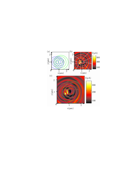
Figures 2(c,d) show a more detailed current map taken at a lateral distance of about from the center of the individual dots, where the distorted hexagon pattern is clearly visible. Along each ring section, distinct spots of enhanced current, corresponding to the pairs of triple points, can be distinguished. The hexagonal pattern is highlighted. It is significantly distorted compared to the corresponding measurement in the plane of two gate voltages because the tip-dot lever arms depend strongly on the tip position. For four hexagon regions, the number of electrons for each dot is indicated. The green cross in the image indicates the position at which the tip was located to record the charge stability diagram shown in Fig. 2(b), whereas the green cross in Fig. 2(b) marks the voltage settings used to record this current map. Therefore the labeled hexagons in Fig. 2 (b) and (d) correspond to the same charge states of the double quantum dot system.
To summarize, our observations are the following: First, we are able to distinguish two sets of rings in the current maps, both of which are concentric around one of the two quantum dots. We are therefore able to directly determine the apparent electronic separation of the two dots in the sample plane. Second, by combining charge stability diagrams with conductance maps, we are able to assign a certain electron number on the double dot to a spatial position of the tip. Finally, we observe a high number of Coulomb peaks (more than 30 in a scan frame depending on, among other things, the tip-sample separation ), letting us conclude that the quality of our tip is excellent.
IV Transition from Single to Double dot
In addition to tuning the double dot with the plunger gates PG1 and PG2, we can also tune the tunnel barriers using STG and DTG. All previous measurements are performed in a region where both barriers are tuned to the tunneling regime, leading to a display of Coulomb blockade in both dots. Using one of the tunnel barrier gates, we can tune only one dot to the Coulomb blockade regime, whereas the other dot is open, forming an extension of the respective contact. With this method we can confine either dot 1, or dot 2 or both dots simultaneously in this double-dot geometry.
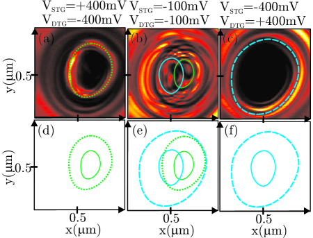
Figure 4 (a) through (c) show current maps recorded for these three regimes. For (a), only dot 2 is confined by the central tunneling barrier and the tunneling barrier near DTG. We observe only a single set of concentric conductance rings. One of these rings is highlighted with a green dotted line and also shown in (d). In Fig. 4(b), we observe clear double-dot behavior. We recognize two sets of concentric rings. Two single resonances are highlighted for clarity. The solid, blue line marks a resonance of dot 1 and the solid, green line marks a resonance of dot 2. When only the dot 1 is confined we observe again single conductance rings as visible in (c). The single resonance traced with a blue, dashed line is shown in Fig. 4 (f). Comparing the 4 traced resonances from Fig. 4 (a-c) in Fig. 4 (e), we observe that the centers of the two blue resonances coincide as do the centers of the two green resonances. These measurements demonstrate that we can establish the position of each single dot in real space. Furthermore, we learn that the position of such a single dot is not changed above the spatial resolution of this measurement, when a second dot is established close to it.
V Influence of the gates in real space on the single dots
In order to investigate the influence of the plunger gate voltages on the double dot, we will now show single line scans, where each line scan is recorded at a different gate voltage. This leads to measurements of the current versus a spatial direction such as x or y and one gate voltage (, , , , ). These measurements contain the information of a series of current maps in a very condensed way. The real space axes are chosen as follows: One line labeled (A) in Fig. 3(b) traverses dot 1 and dot 2 in x-direction. The other line labeled (B) in Fig. 3(b) is the symmetry axis of the structure in y-direction.
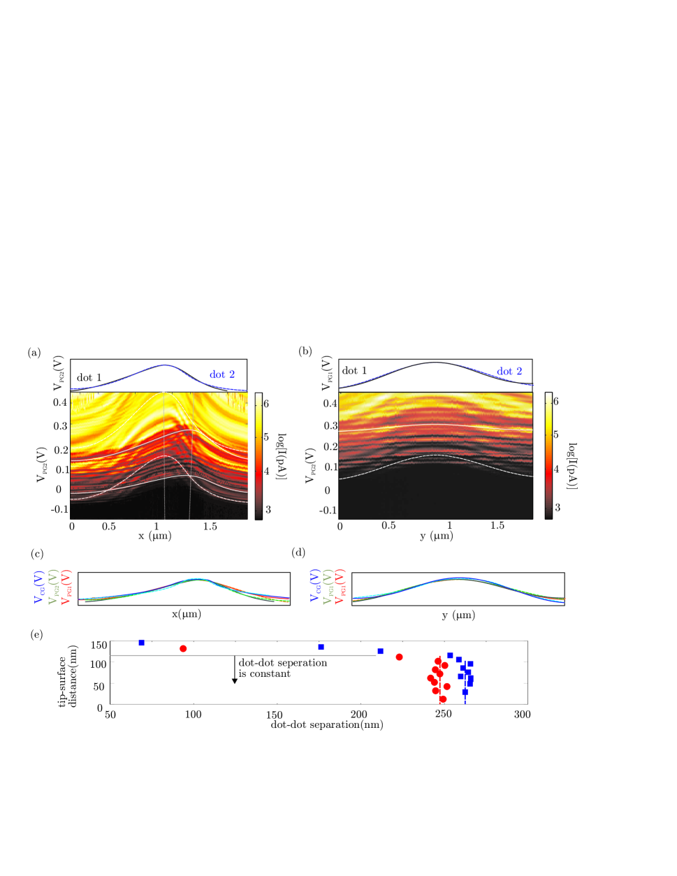
Figure 5 (a) shows . We observe resonances in the current, where we call a single resonance a profile. One profile presents the line of a constant chemical potential in one dot, while in resonance with the leads. Two sets of profiles are visible: one for dot 1 and a second for dot 2. Two profiles of the right set are traced with solid white lines. Two profiles of the left set are traced with white dashed lines. The left profiles belong to dot 1, whereas the right profiles can be attributed to dot 2. Shifting the profiles along the lateral axis and scaling each of these profiles collapses them onto the same curve (see top panel). This confirms that the two dots sense the same tip-induced potential. When increasing the gate voltage, we observe that the amplitude of the profiles increases by a factor of 3 over the measured voltage range. This is due to the gate voltage dependence of the lever arm. For higher gate voltages the lever arm becomes smaller, therefore the voltage increase needed to cause a particular energy shift of a quantum dot level becomes larger, leading to profiles with a bigger amplitude. Furthermore we observe that the amplitude of the profile of dot 2 is a factor of two to three smaller, than the amplitude of the profile related to dot 1 in the same -range. This is because dot 2 is located next to PG2, which has a higher lever arm on dot 2 than on dot 1, leading to a relative lever arm ratio . When sweeping we mainly influence dot 2.
We now investigate the x-position of the maximum of the profile for different . When applying an increasingly positive voltage to PG2, we expect that dot 2 will shift to, or extend towards this gate. This becomes visible in the measurements as a lateral shift of the profiles belonging to dot 2. We observe that the maxima of the profiles of dot 1 stay at the same x-position. However, with increasing gate voltage the maxima of the profiles of dot 2 shift towards PG2 by about . This shift is indicated by the grey dashed line which follows the maxima of the profiles of either dot.
When sweeping the tip along the symmetry axis of the structure, we obtain as shown in Fig. 5 (b). Again we observe two sets of profiles with different amplitudes. For better visibility a profile for each dot is traced with a white line. We find that the profile belonging to dot 1 (dashed white line) has a higher amplitude than the one belonging to dot 2 (solid white line). However, their shape is the same as can be seen in the header. Furthermore, we do not observe a shift in space when sweeping the plunger gate voltage. We can conclude that the apparent y-position of the double dot is not influenced by the gate voltage applied to PG2.
Analogous observations are made by sweeping and (not shown). The shape of the profiles of dot 1 and dot 2 remains the same for all gates evaluated as shown in Fig. 5(c,d) for , and .
The experimental data can be summarized as follows: First, we can observe profiles of the same shapes for both individual dots independent of the gate swept. Second, we can determine the increase in lever arm by the change in amplitude of the resonances for increasing gate voltages as well as the relative lever arms of the gates. And finally, we can quantify the apparent shift of the individual dots due to the increased voltage on a gate, which is in the order of ten to twenty nanometer per volt.
An obvious interpretation of this shift is, that a change in the position of the maximum of the profile allows us to measure by how much the distribution of confined electrons can be shifted in real space by an in plane gate. Although this is qualitatively correct, we have to keep in mind, that such a quantitative deduction of the shift of the electron distribution from the profile maximum might be more complex. In the presence of a scanning gate quantities such as the lever arm, charging energies and the discrete single-particle quantum levels may depend on the position of the tip Kicin_NewJPhys2005 ; Pioda_PRL_2004 . It is therefore hard to decide without a thorough self-consistent approximate numerical solution of the problem, which of these quantities, contributes to the apparent shift of the maxima observed in the experiment.
In order to make sure that the observed shift is a robust and meaningful experimental quantity we carried out z-dependent measurements.
To do so we recorded sets of current maps, where for each subsequent current map we scanned the tip at an increased tip-sample separation, while all voltage settings were kept the same. From each current map the coordinates of positions of both dots were extracted as follows: Each set of rings was fitted with a series of ellipses. We observe that not all ellipses have the same center point, but rather follow a linear shift. This can be attributed to the not perfectly symmetric shape of our tip. Via linear regression we determined the coordinate at which an ellipse of zero major axis length would form. This evaluation is repeated for the second set of ellipses. The parameter evaluated is the distance between the coordinate for dot 1 and dot 2, which we call the apparent dot-dot separation . Determining this relative position makes the evaluation robust against shifts of the complete scan frame. The red dots in Fig. 5(e) show the result of such a series. We see that when changing the tip-sample distance, the observed dot-dot separation remains constant as long as the tip-sample separation is below . For larger tip-sample separations this evaluation becomes unprecise due to the decreased number of Coulomb rings per scan frame as well as the broadening of the individual Coulomb rings in real space. This, together with the decreasing resolution of the measurements leads to a drop in the observed dot-dot separation for tip-sample distances above this value. However, all measurements presented here are carried out well below this threshold. Therefore, the observed shift is a robust experimental quantity independent of below the given limit.
When we carried out the same measurement and evaluation for more positive voltages applied to both plunger gates, we obtain the data set marked with blue squares. Again the dot-dot separation is independent of the tip-sample separation below a certain threshold value. For this measurement we observe an increased dot-dot separation compared to the separation extracted from the first set of current maps. The change in dot-dot separation extracted from these measurements is in the order of about . This is on the same order of magnitude as the shift extracted from the -maps discussed above.
VI Conclusion
We have performed scanning gate measurements on an intentionally formed and fully controllable GaAs double quantum dot. Our experiments give spatially resolved access to the microscopic electronic properties of a double quantum dot. They allow us to locally manipulate the electron number of the individual dots. This measurement technique lets us derive the positions of both quantum dots in real space and evaluate the relative shift of their positions due to in plane gate voltages. We showed that we can also deliberately form a single dot at different positions inside the defined structure by applying different gate voltages. The position of a single dot is not altered above measurement resolution when a second dot is created next to it.
We would like to thank the FIRST Laboratory at the ETH Zurich for their support. We acknowledge financial support by ETH Zurich [TH-20/05-2] and the Schweizerischer Nationalfonds.
References
References
- (1) M. A. Topinka, B. J. LeRoy, R. M. Westervelt, S. E. J. Shaw, R. Fleischmann, E. J. Heller, K. D. Maranowski and A. C. Gossard, Nature 410, 183 (2001).
- (2) A. Pioda, S. Kicin, T. Ihn, M. Sigrist, A. Fuhrer, K. Ensslin, A.Weichselbaum, S. E. Ulloa, M. Reinwald and W. Wegscheider, Physical Review Letters 93, 216801 (2004).
- (3) G. A. Steele, R. C. Ashoori, L.N. Pfeiffer and K. W. West, Physical Review Letters 95, 136804 (2005).
- (4) R. Crook, J. Prance, K. J. Thomas, S. J. Chorley, I. Farrer, D. A. Ritchie, M. Pepper, C. G. Smith, Science 312, 1359 (2006).
- (5) B. Hackens, F. Martins, T. Ouisse, H. Sellier, S. Bollaert, X. Wallart, A. Cappy, J. Chevrier, V. Bayot, and S. Huant, Nature Physics 312, 826 (2006).
- (6) A. C. Bleszynski-Jayich, L. E. Froberg, M. T. Bjork, H. J. Trodahl, L. Samuelson, R. M. Westervelt, Nanotechnology 77, 245327 (2008).
- (7) J. Berezovsky, and et al., Nature Physics 21, 274013 (2010).
- (8) S. Schnez, J. Guettinger, M. Huefner, C. Stampfer, K. Ensslin and T. Ihn, Physical Review B 82, 165445 (2010).
- (9) M. Huefner, C. May, S. Kicin, K. Ensslin, T. Ihn, M. Hilke, K. Suter, N. F. de Rooij and U. Staufer, Physical Review B 79, 134530 (2009).
- (10) A. C. Bleszynski, F. A. Zwanenburg, R. M. Westervelt, A. L. Roest, E. P. A. M. Bakkers and L. P. Kouwenhoven, Nano Letters 7, 2559 (2007).
- (11) M. T. Woodside and P. L. and McEuen, Science 296, 1098 (2002).
- (12) A. Fuhrer, A. Dorn, S. L scher, T. Heinzel, K. Ensslin, W. Wegscheider and M. Bichler, Superlattices and Microstructures 31, 19 (2002).
- (13) W. G. van der Wiel, S. De Franceschi, J. M. Elzerman, T. Fujisawa, S. Tarucha, and L. P. Kouwenhoven, Reviews of Modern Physics 75, 1 (2002).
- (14) M. Reed, J. Randall, J. Luscombe, W. Frensley, R. Aggarwal, R. Matyi, T. Moore, and A. Wetsel, Festkörperprobleme 29, Springer (Berlin/Heidelberg), p267 283 (1989).
- (15) R. Hanson, L. P. Kouwenhoven, J. R. Petta, S. Tarucha and L. M. K. Vandersype, Reviews of Modern Physics 79, 1217 (2007).
- (16) S. Kicin, and et al., New Journal of Physics 7, 185 (2005).
- (17) P. Fallahi, A. C. Bleszynski, R. M. Westervelt, J. Huang, J. D. Walls, E. J. Heller, M. Hanson and A. C. Gossard, Nano Letters 5, 223 (2005).