Majorana Fermions in Semiconductor Nanowires
Abstract
We study multiband semiconducting nanowires proximity–coupled with an s–wave superconductor and calculate the topological phase diagram as a function of the chemical potential and magnetic field. The non-trivial topological state corresponds to a superconducting phase supporting an odd number of pairs of Majorana modes localized at the ends of the wire, whereas the non-topological state corresponds to a superconducting phase with no Majoranas or with an even number of pairs of Majorana modes. Our key finding is that multiband occupancy not only lifts the stringent constraint of one-dimensionality, but also allows having higher carrier density in the nanowire. Consequently, multiband nanowires are better-suited for stabilizing the topological superconducting phase and for observing the Majorana physics. We present a detailed study of the parameter space for multiband semiconductor nanowires focusing on understanding the key experimental conditions required for the realization and detection of Majorana fermions in solid-state systems. We include various sources of disorder and characterize their effects on the stability of the topological phase. Finally, we calculate the local density of states as well as the differential tunneling conductance as functions of external parameters and predict the experimental signatures that would establish the existence of emergent Majorana zero–energy modes in solid–state systems.
I Introduction
The search for Majorana fermions has become an active and exciting pursuit in condensed matter physics Wilczek (2009); Stern (2010); Franz (2010); Nayak (2010). Majorana fermions, particles which are their own antiparticles, were originally envisioned by E. Majorana in 1937 Majorana (1937) in the context of particle physics (i.e., the physics of neutrinos). However, the current search for Majorana particles is mostly taking place in condensed matter systems Levi (2011); Service (2011) where Majorana quasi–particles appear in electronic systems as a result of fractionalization, and as emergent modes occupying non–local zero energy states. The non–locality of these modes provides the ability to exchange and manipulate fractionalized quasiparticles and leads to non–Abelian braiding statistics Nayak and Wilczek (1996); Read and Green (2000); Ivanov (2001); Kitaev (2001); Stern et al. (2004); Nayak et al. (2008); Alicea et al. (2011). Hence, in addition to being of paramount importance for fundamental physics, this property of the Majoranas places them at the heart of topological quantum computing schemes Kitaev (2003); Das Sarma et al. (2005); Stern and Halperin (2006); Bonderson et al. (2006); Bravyi (2006); Nayak et al. (2008); Tewari et al. (2008); Bonderson et al. (2010); Hassler et al. (2010); Sau et al. (2010); Bonderson and Lutchyn (2011); Clarke et al. (2010); Flensberg (2011); Hassler et al. (2011); Jiang et al. (2011); Zilberberg_PRA'08 . We mention that solid–state systems, where the Majorana mode emerges as a zero energy state of an effective (but realistic) low–energy Hamiltonian, enable the realization of the Majorana operator itself, not just of the Majorana particle. Consequently, Majorana physics in solid–state systems is in fact much more subtle than originally envisioned by E. Majorana in 1937. For example, in condensed matter systems the non–local non–Abelian topological nature of the Majorana modes that are of interest to us is a purely emergent property.
About ten years ago, Read and Green Read and Green (2000) discovered that Majorana zero-energy modes can appear quite naturally in 2D chiral p–wave superconductors where these quasiparticles, localized at the vortex cores, correspond to an equal superposition of a particle and a hole. A year later, Kitaev Kitaev (2001) introduced a very simple toy model for a 1D Majorana quantum wire with localized Majorana zero–energy modes at the ends. Both these proposals involve spinless p–wave superconductors where one can explicitly demonstrate the existence of Majorana zero-energy modes by solving the corresponding mean field Hamiltonian. Recently, several groups Fu and Kane (2008); Sau et al. (2010a) suggested a way to engineer spinless p–wave superconductors in the laboratory using a combination of strong spin–orbit coupling and superconducting proximity effect, thus opening the possibility of realizing Majorana fermions in solid–state systems to the experimental field. The basic idea of the semiconductor/superconductor proposal Sau et al. (2010a) is that the interplay of spin–orbit interaction, s–wave superconductivity and Zeeman spin splitting could, in principle, lead to a topological superconducting phase with localized zero–energy Majorana modes in the semiconductor. Since then, there have been many proposals for realizing solid–state Majoranas in various superconducting heterostructures Das Sarma et al. (2006); Fu and Kane (2008, 2009); Wimmer et al. (2010); Sau et al. (2010a); Lee (2009); Alicea (2010); Lutchyn et al. (2010); Oreg et al. (2010); Sau et al. (2010b); Lutchyn et al. (2011); Mao et al. (2011); Potter and Lee (2010, 2011); Qi et al. (2010); Linder_PRL10 . Among them, the most promising ones involve quasi–1D semiconductor nanowires with strong spin–orbit interaction proximity–coupled with an s–wave superconductor Lutchyn et al. (2010); Oreg et al. (2010); Lutchyn et al. (2011). The main advantage of this proposal is its simplicity: it does not require any specialized new materials but rather involves a conventional semiconductor with strong Rashba coupling such as InAs or InSb, a conventional superconductor such as Al or Nb, and an in-plane magnetic field. High quality semiconductor nanowires can be epitaxially grown (see, for example, Ref. Nadj-Perge et al. (2010) for InAs and Ref. Nilsson et al. (2009) for InSb) and are known to have a large spin–orbit interaction strength as well as large Lande -factor ( Aleshkin et al. (2008) and Nilsson et al. (2009)). Furthermore, these materials are known to form interfaces that are highly transparent for electrons, allowing one to induce a large superconducting gap Doh et al. ; van Dam et al. ; Chrestin et al. (1997). Thus, semiconductor nanowires show great promise for realizing and observing Majorana particles Levi (2011); Service (2011). It is important to emphasize that in the superconductor–semiconductor heterostructures the Majorana mode is constructed or engineered to exist as a zero–energy state, and as such, it should be experimentally observable in the laboratory under the right conditions.
In a strictly 1D nanowire in contact with a superconductor, the condition for driving the system into a topological superconducting phase Lutchyn et al. (2010); Oreg et al. (2010) is , where is the Zeeman splitting due to the in–plane magnetic field, is the chemical potential and is the proximity–induced superconducting gap. Thus, the key to the experimental realization of Majorana fermions in this system is the ability to satisfy a certain set of requirements that ensures the stability of the Majorana bound states. The challenging task here is the ability to suppress effects of disorder, control chemical potential fluctuations as well as fluctuations of other parameters. Given that realizing single channel (or one subband ) nanowire is quite challenging, it is natural to consider semiconductor nanowires in the regime of multi–subband occupancy. It was shown in Ref. Lutchyn et al. (2011) that this is a promising route and the existence of Majorana fermions does not require strict one dimensionality. In fact, the stability of the topological superconducting phase is enhanced in multiband nanowires due to the presence of “sweet spots” (multicritical points in the topological phase diagram, see Ref. Lutchyn and Fisher (2011) for details) in the phase diagram where the system is most robust against chemical potential fluctuations Lutchyn et al. (2011). In this paper, we expand on these ideas and explore effects of various perturbations such as disorder in the superconductor and semiconductor, fluctuations in the tunneling matrix elements, etc. on the stability of the topological phase. Our goal is to identify parameter regimes favorable for the exploration of the Majorana physics in the laboratory. We therefore use realistic physical models and realistic values of the parameters throughout this work so that our theoretical results are of direct relevance to experiments looking for Majorana modes in nanowires.
The paper is organized as follows. We begin in Sec. II by introducing a tight–binding model for the semiconductor nanowires, and derive the superconducting proximity effect. We show that electron tunneling between semiconductor and superconductor leads to important renormalization of the parameters in the semiconductor. In Sec. III, we calculate the low-energy spectrum in the regime of multiband occupancy and identify the topological phase diagram. In Sec. IV, we study disorder effects on the stability of the topological phase. We consider several sources of disorder: short–range impurities in the superconductor, short–range and long–range impurities in the semiconductor as well as fluctuations in the tunneling matrix elements across the interface. In Sec. V, we present results for experimentally observable quantities (e.g., local density of states and tunneling conductance) calculated using realistic assumptions. Finally, we conclude in Sec. VI with the summary of our main results.
II Tight–binding model for semiconductor nanowires
II.1 Spin–orbit interaction and Zeeman terms
Single–channel semiconductor (SM) nanowires have been recently proposedLutchyn et al. (2010); Oreg et al. (2010) as a possible platform for realizing and observing Majorana physics in solid state systems. Obtaining strictly one-dimensional (1D) nanowires would raise significant practical challengesDoh et al. ; van Dam et al. , but this requirement can be relaxed to a less stringent quasi–1D condition corresponding to multiband occupancyLutchyn et al. (2011). The physical system proposed for studying Majorana physics consists of a strongly spin-orbit interacting semiconductor, e.g., InAs and InSb, proximity-coupled to an s-wave superconductor (SC). The quasi–1D SM nanowire is strongly confined in the direction, so that only the lowest corresponding sub-band is occupied, while the weaker confinement in the direction is consistent with a few occupied sub-bands. Consequently, the linear dimensions of the rectangular nanowire satisfy the relation which is the usual physical situation in realistic semiconductor nanowires. The low-energy physics of the SM nanowire is described by the Hamiltonian
| (1) | |||||
where includes the first two terms and describes hopping on a simple cubic lattice with lattice constant and the last term represents the Rashba spin-orbit interaction (SOI). We include only nearest-neighbor hopping with , where are the nearest–neighbor position vectors. In Eq. (1), represents a spinor with being electron creation operators with spin , is the chemical potential, is the Rashba coupling constant, and are Pauli matrices. In the long wavelength limit, , our model reduces to an effective mass Hamiltonian with and Rashba spin-orbit coupling , where . In the numerical calculations we use a set of parameters consistent with the properties of InAs, Å, , and eVÅ. The position within the cubic lattice is described by with . In the calculations we have used , , and between and , which corresponds to a nanowire with dimensions nm, nm, and between m and m.
A brute force diagonalization of Hamiltonian (1) on a lattice containing more than sites would be numerically very expensive. More importantly, the relevant energy scales in the problem are of the order of a few meV allowing to construct the low-energy model as we show below and significantly reduce the Hilbert space. The largest energy scale is given by the gap between the lowest sub-bands, which, for example, for the first and second subband and the parameters used in our calculation is meV. Consequently, we are only interested in the low-energy eigenstates of the Hamiltonian (1). To obtain these states, we take advantage of the fact that the eigenproblem for can be solved analytically and notice that can be treated as a small perturbation. Explicitly, the eigenstates of are
| (2) |
where with , and is an eigenstate of the spin operator. The corresponding eigenvalues are
| (3) |
where the chemical potential in the semiconductor is calculated from the bottom of the band. We project the quantum problem into the low-energy subspace spanned by the eigenstates with energies below a certain cutoff value, , where the cutoff energy is typically of the order meV, i.e., one order of magnitude larger than the inter sub–band spacing. The number of states in this low-energy basis is of the order and thus the numerical complexity of the problem is significantly reduced. The matrix elements of the SOI Hamiltonian are
| (4) | |||||
where the second term in the parentheses is obtained from the first term by exchanging the and indices.
To realize nontrivial topological states that support Majorana modes, it is necessary that an odd number of sub-bands be occupied. Lutchyn et al. (2011) In the simplest case of a single sub-band nanowire, this can be achieved with the help of a Zeeman field (i.e. a spin splitting )
| (5) |
which opens a gap at small momenta and removes one of the helicities that characterize the spectrum of a Rashba-coupled electron system. In the multi-band nanowires the situation is more complicated (see below) but the Zeeman term is essential to avoid fermion doubling. The Zeeman term can be obtained using an external magnetic field applied along the axis, . When the chemical potential lies within one of the Zeeman gaps at , the condition for odd sub–band occupation is satisfied and thus fermion doubling is avoided, which allows for the existence of Majorana modes at the ends of the nanowire. Note that in SM with a large g-factor, e.g., and , relatively small in-plane magnetic fields can open a sizable gap without significantly perturbing superconductivity. This is a crucial ingredient of the present proposal which is particularly important in the context of the effect of disorder on the topological phase as we discuss in Sec. IV. For example, in InAs a magnetic field T corresponds to meV. Finally, we note that in the basis given by Eq. (2) the Zeeman term has the simple form
| (6) |
where .
II.2 Proximity–induced superconductivity
In addition to spin-orbit interaction and Zeeman spin splitting, the only other physical ingredient necessary for creating the Majorana mode is the ordinary s-wave superconductivity which can be induced in the semiconductor by the proximity effect, through coupling to an s-wave superconductor (SC). A model of the full system that supports the Majorana modes contains, in addition to the nanowire and Zeeman terms, Eqns. (1) and (5), respectively, the Hamiltonian for the superconductor, , and a term describing the nanowire–SC tunneling, . We note that, to account quantitatively for the superconductivity induced in the nanowire, one should also include possible electron-phonon and electron-electron interactions within the SM itself, . These interactions may enhance or inhibit the induced effect, depending on the details of the SM material DE GENNES (1964); Alexandrov and Kabanov (2008). In this paper we do not take into account effect of interactions in the semiconductor on the proximity effect and use a simple model for the proximity effect using tunneling Hamiltonian approach McMillan (1968) which is appropriate for the sample geometry considered here (thin semiconductor lying on top of the superconductor). The effects of interactions on the topological superconducting phase were recently considered in Refs. Gangadharaiah et al. (2011); Sela et al. (2011); Lutchyn and Fisher (2011); Stoudenmire et al. (2011). In addition to affecting the proximity-induced SC gap, the repulsive Coulomb interactions among the SM electrons lead to an effective enhancement of the Zeeman splitting which might be favorable for inducing topological superconductivity Stoudenmire et al. (2011).
Thus, the total Hamiltonian for our model of semiconductor/superconductor heterostructure is given by
| (7) |
where the tunneling term reads
| (8) |
with and being electron destruction operators acting within the SM and SC, respectively. We assume that the matrix elements couple the sites of the SC located at the interface, , where is position vector in a plane parallel to the interface and is the coordinate of the interface layer in a slab geometry, to the first layer of the semiconductor wire, .
The proximity effect can be now derived by integrating out superconducting degrees of freedom in Eq. (7) and considering the resulting effective low-energy theory for the SM. To identify the form of the effective low-energy Hamiltonian, we consider first the case of a single-band SM coupled to an s–wave SC through an infinite planar interface, then we address the specific issues related to multiband nanowires.
II.2.1 Infinite planar interface
Within the tunneling Hamiltonian approach, the proximity-effect induced by an s-wave SC can be captured by integrating out the superconducting degrees of freedom and calculating the surface self-energy due to the exchange of electrons between SC and SM Sau et al. (2010c). We briefly review this approach here and use these results later when discussing the disordered s-wave superconductors. The interface self-energy is given by
| (9) |
where is the matrix describing tunneling between semiconductor and superconductor. To illustrate the basic physics, we use here the simplest form for tunneling matrix elements with and denoting in-plane and out-of-plane coordinates. After some algebra, the surface self-energy is given by
| (10) |
and finally becomes in the momentum space
| (11) | ||||
| (12) |
where is half bandwidth. The density of states is usually a weakly-dependent function of momenta and energy with and being the Fermi level in the superconductor. With these approximations, the surface self-energy becomes
| (13) | ||||
| (14) |
In the homogeneous case the last term in Eq. (13) represents a shift of the chemical potential and can be neglected as the chemical potential should be determined self-consistently by solving the appropriate equation for the fixed total electron density.
We can now include the surface self-energy into the SM Hamiltonian and study the effective low-energy model for the semiconductor. This can be done by investigating the poles of the SM Green’s function
where , is the Rashba coupling, the strength of a Zeeman field oriented perpendicular to the interface, is the value of the superconducting gap inside the SC, and is the effective SM-SC coupling. In the calculations, in addition to the values specified in Sec. II.1, i.e., and eVÅ, we have meV. The effecting coupling depends on the transparency of the interface, , the amplitude of the SM wave function at the interface, , and the local density of states of the non-superconducting metal at the interface, which can be expressed in terms of the half-bandwidth and the Fermi energy of the metal.Sau et al. (2010c) Note that the Green’s function (II.2.1) is written in the Nambu spinor basis using the Pauli matrices and that correspond to the Nambu and spin spaces, respectively. The identity matrices and are omitted for simplicity.
Explicit comparison between the effective theory described by Eq. (II.2.1) and microscopic tight–binding calculationsSau et al. (2010c) has shown remarkable agreement. A similar effective description has proven extremely accurate in describing the proximity effect induced at a topological insulator – superconductor interface.Stanescu et al. (2010) Can the low–energy physics contained in Eq. (II.2.1) be captured by an effective Hamiltonian description? To address this question, we determine the poles of the Green’s function at frequencies within the superconducting gap, , i.e., we solve the Bogoliubov–de Gennes (BdG) equation . Explicitly, we have
| (16) | |||||
Note that we have considered only the lowest energy mode. In Eq. (16) dynamical effects are generated by the frequency dependence of the proximity–induced terms containing the expression , with a relative magnitude that depends on the SM-SC coupling strength. In general, we distinguish a weak-coupling regime characterized by and a strong coupling regime, . In the weak coupling regime we expect negligible dynamical effects at all energies that are not very close to the gap edge, . Neglecting the frequency dependence in the proximity–induced terms, the solution of Eq. (II.2.1) becomes
| (17) |
where is the quiasiparticle residue at zero energy.
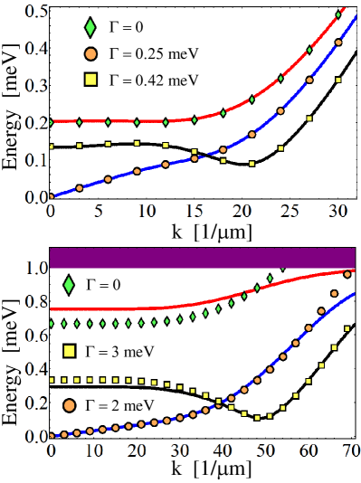
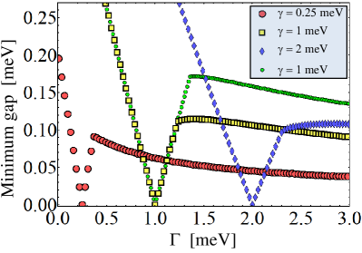
To evaluate the dynamical effects, we compare the BdG spectrum given by Eq. (17) with the full solution of Eq. (16). The results are shown in Fig. 1 for a weak coupling regime characterized by meV (top panel) and at large coupling, meV (bottom panel). Notice that, even for effective couplings larger than the gap, e.g., , Eq. (17) represents a very good approximation of the low energy spectrum. What about couplings that are much larger than ? To answer this question, let us consider the dependence of the low–energy spectrum on the coupling constant , and the Zeeman field . For the spectrum is gaped and the minimum of the gap is located at (see Fig. 1). Applying a Zeeman field reduces this minimum gap continuously and at the critical value the spectrum becomes gapless (see Fig. 1). For a gap opens again with a minimum at for and at a finite wave vector for large values of the Zeeman field. The dependence of the minimum gap on the Zeeman field is shown in Fig. 2 for three different values of the SM-SC coupling. The vanishing of the gap at the critical point marks a quantum phase transition from a normal SC at low Zeeman fields to a topological SC ( when ).Lutchyn et al. (2010); Sau et al. (2010c) The change in the location of the quasiparticle gap from to a finite wave vector is marked in Fig. 2 by a discontinuity in the slope at . The optimal value of the excitation gap in the topological phase is obtained for . This optimal value depends weakly on the effective coupling , but varies strongly with the spin–orbit coupling.
From the above analysis we conclude that the strong–coupling regime characterized by is not experimentally desirable, as it would require extremely high magnetic fields to reach the topologically nontrivial phase, i.e., . In addition, it would be difficult to tune the chemical potential and drive the system into a topological superconducting phase for a large SM-SC coupling. Also, as follows from Eq. (17), the quasiparticle excitation spectrum decays with increasing which leads to the reduced stability of the topological phase against thermal fluctuations. Hence, an experimentally useful interface should be characterized by an effective coupling of order or less, i.e., in the intermediate to weak–coupling regime. As shown above, in these regimes the BdG spectrum is accurately approximated by Eq. (17). Consequently, we can model the low–energy spin–orbit coupled semiconductor with proximity induced superconductivity using an effective tight–binding model given by the Hamiltonian
| (18) |
where the semiconductor term has the same form as the Hamiltonian for the nanowire given by Eq. (1) but with and and the Zeeman term is given by Eq. (5) with . In addition, all the energy scales are renormalized by a factor , i.e., , , etc. The physical meaning of the factor written as is intuitively clear - it corresponds to a probability to find an electron in the semiconductor. The induced superconductivity is induced by the effective pairing term
| (19) |
with an effective SC order parameter . With these choices, given by Eq. (18) has the same low energy spectrum as the one described by Eq. (17).
II.2.2 The multiband case
To account for the specific aspects that characterize the proximity effect in finite–size systems, we return to the details of deriving the effective low–energy Green’s function description, e.g., Eq. (II.2.1), starting with the microscopic Hamiltonian (7). After integrating out the SC degrees of freedom, the effective SM Green’s function acquires a self–energy
where are the orbital components of the eigenstates described by Eq. (2) and is the SC Green’s function, both evaluated at the interface. In Eq. (II.2.2) and are matrix elements that couple two sites with in–plane coordinates across the interface. In the discussion of the planar interface we implicitly assumed translational invariance for the coupling, i.e., . Here, we consider position–dependent couplings and argue that engineering interfaces with a transparency that varies across the wire, i.e., , generates off–diagonal components of the effective SC order parameter that help stabilize the Majorana modes.Lutchyn et al. (2011) We note that variations of the coupling matrix element along the wire, i.e., in the direction, act as an effective disorder potential. We will address this issue below in Sec.IV.3.
The SC Green’s function integrated over momenta can be written explicitly as (see Eq. (13))
| (21) |
where with being the half-bandwidth, being the Fermi energy and meV being the s-wave SC gap. In the numerical calculations we have , i.e., . Using the expression of the SC Green’s function given by Eq. (21), the self-energy (II.2.2) becomes
| (22) |
with the implicit assumption that the wire is very thin, , and . The coupling matrix in Eq. (22) is
| (24) |
We note that for position–independent SM–SC couplings, , the matrix is proportional to the unit matrix and the effective low–energy Hamiltonian can be obtained along the lines of Sec. II.2.1. However, for non–uniform couplings, acquires off–diagonal elements that generates normal and anomalous inter–sub–band terms in the effective Hamiltonian via the self–energy (22). The relative magnitude of the off–diagonal terms depends on the non-homogeneity of the SM–SC coupling. To quantify this property, we consider a fixed profile with the property and and the position–dependent tunneling , where is a parameter that measures the degree of non–uniformity of the coupling. Shown in Fig 3 (upper panel) is for .
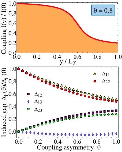
As we show below, the non–uniform coupling induces an effective pairing , where is given by Eq. (24). The dependence of on the coupling asymmetry parameter is shown in Fig 3 (lower panel). For uniform tunneling () the off–diagonal elements vanish and the diagonal elements become equal. By contrast, strongly non-homogeneous tunneling () generate off–diagonal terms that reach about of the diagonal contributions for neighboring sub–bands, , and are much smaller for .
The low–energy effective Hamiltonian for the nanowire can be derived following the scheme described in Sec. II.2.1. As before, at low energies () we can neglect the frequency dependence of the dynamically–generated terms, i.e., . However, due to the inter–sub–band coupling induced by non–homogeneous proximity effect, one cannot simply renormalize the energy by a factor . This is due to the fact that the Green’s function for the proximity–coupled nanowire, , contains a frequency–dependent term that is not proportional to the unit matrix. However, we notice that we can define a matrix with the property . Explicitly, we have
| (25) |
where is given by Eq. (24) and . Because , the renormalized Green’s function satisfies the same BdG equation as the original Green’s function, i.e., . We conclude that the low–energy physics of a nanowire proximity–coupled to an s–wave SC can be described by an effective Hamiltonian that can be conveniently characterized by its matrix elements in the Nambu basis provided by the eigenstates of given by Eq. (2). Considering only the lowest band, i.e., , we can write explicitly
where , , , and summation over the repeating indices , is implied. In Eq. (II.2.2) the matrix is given by Eq. (25), the Hamiltonian for the nanowire is , and the matrix elements of , , and are given by equations (3), (4), and (6), respectively. We note that for a homogeneous SM–SC interface the normal contribution proportional to becomes diagonal and can be absorbed in the chemical potential, but in general it generates inter–sub-band mixing. These induced off–diagonal terms can be significant in the strong–coupling limit. Finally, the effective SC order parameter is
| (27) |
where is given by Eq. (24) and has the same significance as in Eq. (25).
III Low–energy spectrum, Majorana bound states, and phase diagram
III.1 General properties of the BdG spectrum
The effective BdG Hamiltonian (II.2.2) can be written as
| (28) |
where and are renormalized nanowire and Zeeman Hamiltonians, respectively, and is the effective pairing with matrix elements . We note that the normal contribution proportional to from Eq. (II.2.2) is included in . As mentioned above, for homogeneous SM–SC coupling the only effect of this term is to generate an overall shift of the energy. For convenience, we eliminate this shift by adding a term to the effective Hamiltonian (II.2.2), where
| (29) |
is the “average” effective pairing. Note that for and the diagonal contribution to the energy–shifting term is partially canceled even in the non–homogeneous case. Finally, to be able to compare results corresponding to various degrees of inhomogeneity in the coupling, i.e., different parameters, we define the average coupling strength as
| (30) |
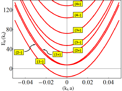
To obtain better insight into the properties of the BdG Hamiltonian, we start with a non-superconducting system described by the Hamiltonian and , i.e., an infinitely long renormalized nanowire placed into an effective magnetic field. The spectrum of the renormalized wire is shown in Fig. 4 for a chemical potential and a Zeeman field , where is the characteristic spin-orbit coupling energy. Here and below we systematically use as energy unit. The bare nanowire spectrum is renormalized due to a weak inhomogeneous coupling with a profile given in Fig. 3, , and . For the sub–bands with a given value of are double degenerate at , but this degeneracy is removed by the Zeeman field. However, for special values of , sub–bands corresponding to different values of may become degenerate at (see Fig. 4). If the chemical potential has a value such that the degeneracy point occurs at zero energy, represent a so–called “sweet spot”.Lutchyn et al. (2011) Adding superconductivity, will now open a gap in the spectrum near . In the weak–coupling limit, one can determine the topological nature of the induced superconductivity by simply counting the number of sub–bands crossed by the chemical potential: an odd number corresponds to a topologically non-trivial SC, while an even number results in a standard superconductor.Lutchyn et al. (2011) Within this simplified picture, the “sweet spots” represent critical points. As will be shown below, the properties of the system in the interesting parameter regimes near the “sweet spots” are determined by the effective inter–band pairing, i.e., by the non–homogeneity of the SM–SC proximity effect.
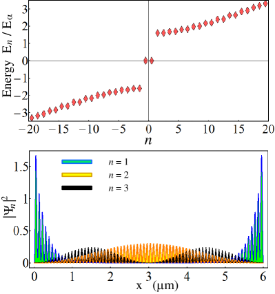
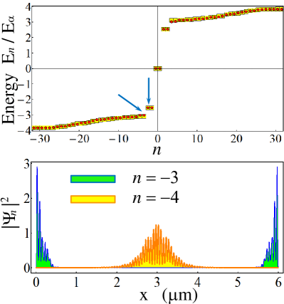
Next, we diagonalize numerically the full effective Hamiltonian (II.2.2) for a finite wire using the same set of control parameters, and . The corresponding low–energy spectrum is shown in the upper panel of Fig. 5. The eigenstates are labeled by an integer number n that has the same sign as the corresponding eigenvalue . The spectrum is characterized by a gap and a pair of zero–energy Majorana bound states. To prove the localized nature of these states, we calculate the wave function amplitude and show that the Majorana modes are localized near the ends of the wire (Fig. 5 lower panel). By contrast, finite energy states extend over the entire system. The oscillations of the wave function amplitudes is associated with the Fermi momentum , as shown in Fig. 4. We note that amplitudes shown in Fig. 5 represent the particle component of the BdG wave-functions, i.e., . For a finite-energy state, e.g., the corresponding total spectral weight is about , with the other half coming from from . The Majorana modes have a total weight of one, which corresponds to one physical particle, but this weight is spatially separated into two contributions localized near the ends of the wire. Removing the Majorana pair would require overlapping the two components, which cannot be done by local perturbations. This is, of course, the topological immunity of the Majorana modes, which is crucial for topological quantum computation. The characteristic length scale for the localized modes is controlled by the minimum value of the quasi–particle gap in a wire with no ends, e.g., with periodic boundary conditions, . As will be shown below (see Sec III.3), in a finite wire it is possible that bound states localized near the ends of the system have energies within the gap. When in–gap states are present, the lowest–energy localized state sets the value of the mini–gap, . We emphasize that for a set of control parameters corresponding to a non–vanishing minimum quasi–particle gap , the mini–gap is always nonzero. The characteristic length scale for the localized modes diverges in the limit . Hence, the topological phase is protected as long as the quasi–particle gap remains finite. Consequently, to determine the stability of the Majorana bound states, our key task is to determine the dependence of on various physical parameters and experimentally–relevant perturbations, e.g., chemical potential, Zeeeman field, SM–SC coupling, and charged impurity and coupling–induced disorder.
At this point in our analysis it is important to clarify the role played by the parameters that incorporate the SM–SC proximity effect into the low–energy effective theory. In particular, we address the following question: how does the low–energy spectrum depend on the strength of the SM–SC coupling (i.e., on ), on the non-homogeneity of the coupling (), and on the dynamical effects included in the effective description ()? The non-homogeneity of the coupling is responsible for generating inter sub–band pairing in Eq. (27). These off–diagonal contributions play a minor role away from the “sweet spots”, where they generate a small quantitative change of the quasi–particle gap. However, in the vicinity of the “sweet spots” vanishes in the absence of inter sub–band pairing and the non-homogeneity of the coupling (i.e., ) becomes crucial.
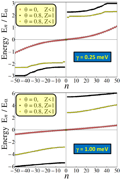
As expected, inclusion of dynamical effects through renormalizes the energy scales. Without these effects, the mini–gap would increase monotonically with the coupling strength, but dynamical effects limit its maximum value. The optimal quasi–particle gap obtains in the intermediate coupling regime . Further increase of the coupling leads to a decrease of the gap. To illustrate the features described above, we show in Fig. 6 low–energy spectra in the vicinity of the “sweet spot” (, ) at weak coupling (, top panel) and intermediate coupling (, bottom panel). Note that in the absence of inter–band pairing, i.e., for homogeneous SM–SC coupling, the gap near the “sweet spot” collapses. Also, inclusion of dynamical effects at intermediate and strong coupling is the key for obtaining the correct energy scales. Finally, the location of the “sweet spots” in the plane depends on the coupling strength and, more generally, the location of phase boundaries depends on the strength of the SC proximity effect.
III.2 Phase diagram for multi–band superconducting nanowires
Topological superconductivity and, implicitly, the Majorana bound states are protected by the quasi–particle gap , as discussed above. The vanishing of signals a transition between topologically nontrivial and topologically trivial superconductivity. In a multi–band system, such transitions can be caused, for example, by varying the Zeeman field while maintaining a fixed value of the chemical potential. The vanishing of at certain specific values of reveals a sequence of alternating SC phases with trivial and nontrivial topological properties. A natural question is whether different topologically nontrivial (or trivial) phases have exactly the same low–energy properties. While topologically identical, these phases may have have some distinct features, at least in certain parameter regimes.
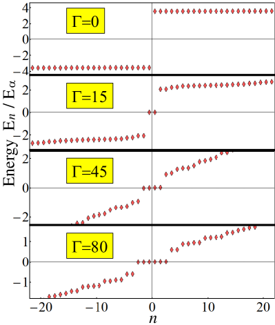
To address this question, we calculate the low-energy spectrum for a system with a fixed chemical potential, , and different values of , one from each of four intervals separated by points characterized by a vanishing gap. The results are shown in Fig. 7. The distinctive feature of the spectra in Fig. 7 is their number of zero–energy modes. In the presence of a very weak Zeeman field, the SC phase has trivial topology and no zero–energy modes. Increasing generates a transition to a topological SC phase characterized by one pair of Majorana bound states. The further increase of the applied Zeeman field produces alternating topologically trivial and nontrivial SC phases with increasing number of zero–energy bound states. Topological SC phases are characterized by an odd number of pairs of Majorana bound states, while trivial SC phases have an even number of pairs.
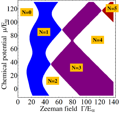
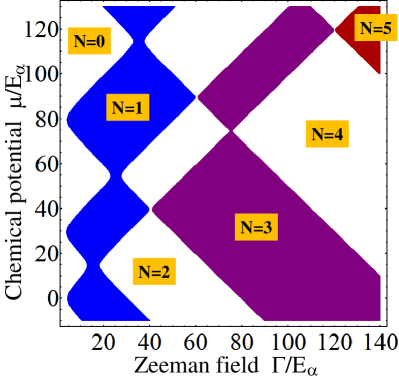
This type of sequence of alternating SC phases is independent of the chemical potential or the strength of the SM–SC coupling. As discussed above, in the weak–coupling limit this behavior can be directly related to the number of sub–bands of an infinite wire that cross the chemical potential: an odd (even) number corresponds to a nontrivial (trivial) topological superconductor. At the phase boundary between two SC phases with different topologies, two sub–bands become degenerate at . In addition, at certain special values of the control parameters and two different phase boundaries intersect leading to multicritical points. We will call these special crossing points x-points. The “sweet spots” mentioned above are examples of such x-points. The key question is how the phase boundaries evolve when we turn on the SM–SC coupling and, in particular, what the physics is in the vicinity of the x-points, see also Ref. Lutchyn and Fisher (2011). To obtain the global phase diagram in the plane, we determine the parameters that satisfy the condition , i.e., we identify the phase boundaries for transitions between topologically trivial and non–trivial phases by imposing the condition of a vanishing quasi–particle gap. We show below that this approach is consistent with the calculation of the topological index (Majorana number) which distinguishes topologically trivial and non-trivial SC phases Kitaev (2001); Lutchyn et al. (2011). The results are shown in Fig.8 for weak coupling () and in Fig.9 for intermediate coupling ().
For (see Fig. 8), the only significant difference as compared to the weak–coupling picture presented above is the disappearance of the phase boundary crossings at the x-points. Instead, the region in the vicinity of these points is occupied by the phase that is robust against variations of the chemical potential. Near the “sweet spots”, this phase is the nontrivial topological SC. We note that the disappearance of phase boundary crossings is a direct result of the off–diagonal pairing induced by a non-uniform SM–SC coupling. Uniform tunneling () does not eliminate the x-points, independent of the coupling strength, but pushes them to higher values of the Zeeman field as increases. Also, we note that the characteristic width of the stable phase in a given avoided crossing region is controlled by a specific off–diagonal component . For example, the “sweet spots” inside the phase characterized by (see Fig. 8) are controlled by the dominant matrix elements (see Fig. 3), while the avoided crossings within the topologically trivial phase are controlled by matrix elements , that are typically smaller. Hence, we expect the strongest effect within the topological phase characterized by one pair of Majorana bound states. As this phase also requires relatively low Zeeman fields, it is the experimentally relevant phase for realizing and observing Majorana fermions. At intermediate couplings, the phase is pushed to slightly higher fields (see Fig. 9). However, as a result of the effective phase space of the “sweet spots“ expanding significantly, this regime presents the remarkable possibility of being able to vary the chemical potential over energy scales of the order meV without crossing a phase boundary. As we will show below, this feature has major experimental implications in the sense that the elusive Majorana mode is most likely to be experimentally realized in the laboratory in this particular physically realistic parameter regime. We note that this interesting parameter regime exists for the multiband situation.
III.3 Dependence of the gap on the Zeeman field and the chemical potential
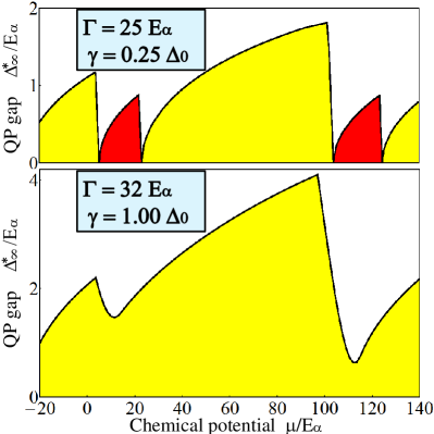
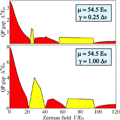
The phase diagram provides information about the topological nature of the phase characterized by given sets of control parameters . However, we are ultimately interested in the stability of the Majorana bound states that occur at the ends of a nanowire within the topologically nontrivial phase. As the Majorana zero–energy modes are protected by the quasi–particle gap, knowing the size of the gap and the dependence of on the control parameters is critical. To address this issue, we determine the dependence of the gap on both the Zeeman field at fixed chemical potential and on at fixed . The results are shown in figures 10 and 11. In general, the gap is non-zero everywhere except at points corresponding to phase boundaries. In the vicinity of a point with the minimum gap in an infinitely long wire occurs at . The dependence of this minimum on the Zeeman field is approximately linear in the deviation from the critical field, (see Fig. 10). This generalizes the single–band results shown in Fig. 2. Note that outside this linear regime, the minimum gap occurs at finite wave vectors. Finally, we note that, at intermediate couplings, the Zeeman field can be tuned so that the gap remains finite over a large range of chemical potentials (Fig. 11, bottom panel). Such regimes are extremely stable against fluctuations of the chemical potential produced by disorder or other perturbations, as we will show explicitly in the next section. We emphasize that the critical ingredients for realizing this regime are: i) the off-diagonal pairing obtained by a non–uniform SM–SC coupling, and ii) an effective average coupling of the order of the bare SC gap . Note that the coupling strength can be controlled by either modifying the tunneling , or by changing the width of the nanowire in the direction perpendicular to the interface with the superconductor.
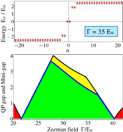
As we mentioned above, the value of the gap in a finite system is, in general, smaller that the minimum gap in a system with the same parameters but no ends, e.g., with periodic boundary conditions. We emphasize that this is not a finite size effect, but is due to the appearance of in–gap states that are localized near the ends of the wire. In the topologically non–trivial phase, the characteristic length scale for these states is the same as that of the Majorana zero modes and, for wires with lengths larger than this scale, their energy is independent of . To illustrate this behavior, we show in Fig. 12 (top panel) the spectrum of a system characterized by , , , and . We notice a pair of zero–energy Majorana modes and a number of states with almost the same energy that are extended over the entire length of the wire, as we checked explicitly. In addition, we notice pair of states with energy within the bulk gap. An analysis of the position dependence of reveals that these states are localized near the ends of the wire. The minimum energy of the extended states is equal to the quasi–particle gap , while the lowest energy of the bound states is equal to the mini–gap . We can understand these bound states as precursors of the extra–pair of Majorana zero–modes that characterize the topologically trivial phase that obtains for . Increasing the magnetic field pushes down the energy of the bound states until it vanishes at the transition, when . On the other side of the transition, an extra–pair of localized states will be characterized by zero energy (see Fig. 7). The evolution of the mini–gap with the Zeeman field is shown in the lower panel of Fig. 12. Note that in the vicinity of the transition points , while deep inside the topological phase . Similar behavior can be observed throughout the phase diagram, including the topologically trivial phases.
III.4 Phase diagram for an effective three–band model using the topological invariant.
In this section we consider an effective three-band toy model which allows one to qualitatively understand several features observed in the detailed numerical simulations discussed in the previous sections.
The topological phase diagram for the multiband nanowire can be obtained analytically using topological arguments due to Kitaev Kitaev (2001). Namely, the superconducting phase hosting Majorana fermions has an odd fermion parity whereas the non-topological phase has even fermion parity. Thus, the phase diagram can be obtained by calculating the topological index (Majorana number) defined as
| (31) |
The change of signals the transition between trivial () and non-trivial phases (). The antisymmetric matrix in Eq.(31) represents the Hamiltonian of the system in the Majorana basis Kitaev (2001) and can be constructed by the by the virtue of particle-hole symmetry Lutchyn et al. (2010); Ghosh et al. (2010). Specifically, the particle-hole symmetry of the BdG Hamiltonian is defined as
| (32) |
where is an anti-unitary operator with and representing unitary transformation and complex conjugation, respectively. One can check that the matrix calculated at the particle-hole invariant points where is indeed antisymmetric . In 1D there are two such points: with being the momentum at the end of the Brillouin zone and being the lattice spacing. The function in Eq. (31) denotes Pfaffian of the antisymmetric matrix . In the continuum approximation, where the lattice spacing and , the value of . Thus, the topological phase boundary given by the change in the topological index is determined by , and, thus, is accompanied by the gap closing at zero momentum. Note that the topological reconstruction of the spectrum is always accompanied by closing of the bulk gap Read and Green (2000) since . Our approach of calculating the TP invariant relies on translational symmetry. Recently, the expression for the TP invariant was generalized to spatially inhomogeneous case Akhmerov et al. (2011); Beenakker et al. (2011).
We now calculate for a simplified three-subband model and compare the phase diagram with the numerical one presented in the previous section. To make progress we assume that , and consider only diagonal in the subband index spin-orbit coupling terms in Eq. (4). With these approximations, becomes
| (33) |
Here represents the energy difference between first and second (third) subbands due to the transverse confinement. The superconducting gaps are related to the nominal bulk gap via relations and which take into account the dependence of the induced parameters on tunneling strength. Here we have chosen a reasonable ratio of . Similarly, all other energies are renormalized in the following way as explained in the previous sections.
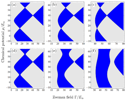
The phase diagram showing a sequence of topological phase transitions for the three sub-band toy model is shown in Fig. 13. The panels (a)-(c) represent the phase diagram with no interband mixing terms (i.e. ). One can clearly see crossings in the phase diagram which represent the “sweet spots”. One can also notice the effect of the renormalization due to SM-SC tunneling as we increase - the superconducting and normal terms are rescaled in a different way as explained above. In the weak-coupling regime , the normal terms are not significantly renormalized since whereas induced pairing is small and is entirely determined by the normal state level broadening . On the other hand, in the strong-coupling regime , the normal terms are decreasing with because whereas saturates at . Thus, strong SM-SC tunneling leads to important quantitative effect which should be taken into account in a realistic model for the proximity effect.
The panels (d)-(f) represent the phase diagram with finite interband mixing terms . Here we find qualitative agreement with the numerical results presented in the previous sections, compare Figs. 8 and 9 with 13 (d) and (e). Different renormalization of the normal and SC terms has a two-fold effect on the phase diagram: a) with the increase of tunneling the topological phase is effectively “pushed” towards higher magnetic fields; b) even small interband pairing term opens a large gap at the sweet spot leading to extended vertical topological regions. This insensitivity of the topological phase against chemical potential fluctuations can be exploited for the protection against disorder in the multisubband occupied nanowires with no such situation arising in the single channel case.
III.5 Phase diagram in the presence of a transverse external potential.
A key feature of the phase diagrams shown above is represented by the hot spots. In the presence of inter sub–band pairing, the topologically nontrivial phases expand in the vicinity of these hot spots, and, for certain values of the Zeeman field, become stable over a wide range of values for the chemical potential. As we show in the subsequent sections, this property is critical for stabilizing the topological superconducting phase and, ultimately, for realizing and observing the Majorana zero modes. The necessary ingredient for obtaining this expansion of the hot spots is a non–vanishing inter–sub–band pairing, which is obtained by a non–uniform SM–SC coupling characterized by a strong position dependence along the direction transverse to the wire (see Fig. 3). The natural question is whether this effect can be obtained by breaking the symmetry in the transverse direction using an external field, e.g., generated by a gate potential, instead of a non–uniform coupling. This would constitute an alternative to engineering non–uniform SM–SC interfaces that would be much simpler to implement and would allow better control. To investigate this possibility, we consider an external potential that varies linearly across the nanowire,
| (34) |
where is the amplitude of the transverse external potential. The matrix elements for the external potential are strictly off–diagonal and couple strongly the neighboring sub–bands, while other contributions are at least one order of magnitude smaller. Consequently, to a first approximation we have , . Even in the presence of this inter–band coupling, the Pfaffian for the effective three–band model can be determined analytically and it is given by an expression that generalizes Eq. (33). The corresponding phase diagrams for both uniform and non–uniform SM–SC couplings and different values of the external potential are shown in Fig. 14.
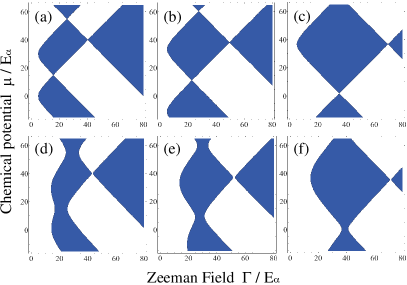
The key conclusion of this calculation is that inter–sub–band mixing due to an external transverse potential does not lead to an expansion of the topological phase in the vicinity of the sweet spots, but rather determine a shift in their position. This is illustrated by diagrams (a-c) in Fig. 14, which correspond to homogeneous SM-SC coupling, i.e., , and different values of the external field. Notice that, to a first approximation, the effect of the transverse potential is equivalent to increasing the inter–sub–band spacing . If the transverse potential is applied across a wire that is non–uniformly coupled to the SC, in addition to shifting the position of the sweet spots, it reduces the stability of the topological phase in their vicinity, as illustrated in panels (d-f) for . In addition, as a consequence of effectively increasing the inter–sub–band spacing, the regions between successive sweets spots occupied by the topological SC phase expands with increasing the transverse potential, as shown in panels (c) and (f). Note that, in the presence of non–uniform SM–SC coupling, the phase diagrams for and (not shown in Fig. 14 are slightly different. The strong dependence of the phase boundaries on the transverse potential, especially in the vicinity of the sweet spots, could be used experimentally for driving the system across the topological phase transition by tuning a gate potential, instead of changing the magnetic field.
IV Effect of disorder on the topological superconducting phase
In this section we consider the effect of disorder on the stability of the topological superconducting phase harboring Majorana fermions. In a realistic system, disorder comes in various ways that affect the topological phase very differently. In this paper we consider three types of disorder: impurities in the s–wave superconductor, short– and long–range disorder in the semiconductor wire, and random nonuniform coupling between the semiconductor wire and the superconductor, which mimics a rough interface and the imprecision in engineering inhomogeneous –dependent couplings. We begin by considering short–range impurities in the bulk superconductor, followed by the consideration of the other two types of disorder which are both more complex to treat theoretically and more detrimental to the existence of the Majorana modes.
IV.1 Short-range impurities in the bulk superconductor.
In order to understand the effect of non–magnetic impurities on the induced superconductivity in the semiconductor, we first review the results on the proximity effect for the infinite planar interface presented in the previous section. The basic idea is that the presence of short–range non–magnetic impurities in the metal modifies the bulk Green’s function, which then is used to derive the appropriate superconducting proximity effect.
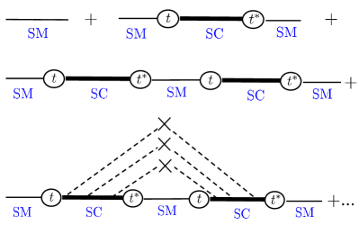
We begin our discussion by considering the perturbation theory in the tunneling , which is justified in the limit of low interface transparency. The lowest order contributions of the diagrammatic expansion in are shown in Fig. 15. One can notice that the self-energy at the second order in is determined by the disorder-averaged Green’s function in the superconductor. Since typical s-wave superconductors are disordered (i.e. with being momentum relaxation time), the effect of impurity scattering is non-perturbative. In general, this yields a non-trivial problem because of the self-consistency condition which now has to be solved in the presence of disorder. The problem, however, can be substantially simplified if we neglect the effect of the in-plane magnetic field on the s-wave superconductivity. This condition can be justified due to the vast difference of the -factors in the superconductor and semiconductor. We also assume here that the superconductor is thin enough so that we can neglect orbital effects. At this level of approximation, the problem reduces to understanding the effect of non-magnetic impurities on the bulk s-wave superconductivity, which has been investigated long time ago by Abrikosov and Gor’kov Abrikosov and Gor’kov (1961). The main result of Abrikosov-Gor’kov’s theory is that disorder does not affect s-wave superconductivity, i.e., the superconducting gap is not suppressed by non-magnetic impurities, in agreement with Anderson’s arguments invoking time-reversal symmetry. Specifically, the disorder at the single-particle Green’s function level merely leads to the renormalization of the parameters and :
| (35) | ||||
| (36) |
Here bar represents disorder–averaged Green’s function and the disorder strength is parameterized by the impurity scattering time defined as with , and being the density of states at the Fermi level, the impurity concentration, and the scattering potential, respectively. Thus, at this level of the perturbation theory, the proximity effect can be included using the formalism developed for the clean case, see Eq. (13). By integrating out the degrees of freedom corresponding to the superconductor, one obtains the interface self-energy:
| (37) | ||||
| (38) |
Finally, upon substituting the expressions for and , we find that proximity–induced superconductivity is not affected by disorder in the s–wave superconductor
| (39) |
Moreover, one can see that, unlike impurities in the semiconductor, the disorder in the superconductor does not lead to momentum relaxation in the semiconductor at this order of the perturbation theory.
As the interface transparency is increased, one needs to consider higher–order terms in tunneling. These terms involve reducible and irreducible contributions, see Fig. 15. The former depend only on the disorder–averaged Green’s function, and, in a sense, are easy to take into account, whereas the latter involve non–trivial higher-order correlation functions (i.e. diffusons and Cooperons) and lead to momentum relaxation in the semiconductor . In this work, we consider only reducible contributions and neglect higher order correlation functions with respect to disorder-averaging which, one can show, are much smaller than the reducible ones Potter_disorder . Therefore, our minimal treatment of the disorder in the superconductor is justified and we believe that the superconducting disorder is irrelevant for the topological superconductivity. However, the disorder in the semiconductor (and at the interface) is relevant, as we discuss next.
This conclusion holds as long as we neglect the effect of external magnetic field on the s–wave superconductivity, which is allowed as long as the field is not too large to destroy the superconducting state. This is realistic due to the large difference between the -factors in superconductors () and semiconductors (), allowing one to always find a parameter regime where the magnetic field opens a large spin gap in the spectrum without destroying superconductivity. Also, note that our conclusion regarding the short–range impurities in the superconductor is valid when the strength of the disorder is much larger than the superconducting gap: but is small enough not to affect the density of states. We have restricted our analysis to the experimentally relevant regime . In the opposite limit , electrons spend most of the time in the s-wave superconductor where their dynamics is not governed by the helical Hamiltonian required to have a topological phase and, thus, this limit is not experimentally desirable, see discussion in Sec. II.2.1.
We emphasize that our finding that short–range impurities in the bulk superconductor do not affect the topological superconducting phase emerging in the semiconductor is quite general since the electrons in the nanowire, being spatially separated from the bulk superconductor, simply do not interact directly with the short–range disorder in the bulk superconductor. Our use of the short–range impurity model to characterize the disorder in the bulk superconductor is justified, since strong metallic screening inside the bulk superconductor would render all bare long–range disorder into screened short–range one. Thus, as long as the applied magnetic field does not adversely affect the s–wave superconductivity, our conclusion regarding the validity of the Anderson theorem (i.e., no adverse effect from non–magnetic impurities) to the whole superconductor–semiconductor heterostructure system applies. In this context, we mention the recent theoretical analysis of Ref. Tewari et al. (2011), where it was explicitly established that, in the structure we are considering, the proximity–induced superconducting pair potential remains s–wave both in the topological and in the non–topological phase, in spite of the non–vanishing Zeeman field. The existence of the s–wave pairing potential, even in the presence of a parallel magnetic field (provided it is not too large), is the key reason for the short–range disorder in the superconductor not having any effect on the topological phase.
IV.2 Disorder in the semiconductor nanowire
In sharp contrast to disorder in the superconductor, disorder in the nanowire can have significant adverse effects on the stability of the topological SC phase. There are several different potential sources of disorder in the semiconductor. We focus on two sources that are the most relevant experimentally: random variations of the width of the SM nanowire and random potentials created by charged impurities. The first type of disorder is generally long–ranged, while the second type can be either long– or short–ranged. How to account for the effects of disorder depends crucially on the type of physical quantity that one is interested in. Here we focus on the low–energy spectrum, which carries information about the stability of the Majorana bound states, and on thermodynamic quantities such as the local density of states, which are experimentally relevant. The effect of disorder on these quantities is sample–dependent. We emphasize that averaging over different disorder realizations is equivalent in this case with sample averaging. As the goal is to observe stable Majorana fermions in a given nanowire, we investigate here the spectrum of the system for a given disorder realization and focus on establishing the general parameter regimes (e.g., amplitudes and length scales of the disorder potential) consistent with realistic experimental conditions that ensure the stability of the topological SC phase. More specifically, we study several different disorder realizations characterized by a given set of parameters and extract the generic features associated with that type of disorder.
For a single channel Majorana nanowire, one can obtain some analytical results by performing disorder averaging Motrunich et al. (2001); Gruzberg et al. (2005); Brouwer et al. (2011a). Specifically, for a model of the spinless p-wave superconductor it has been shown Motrunich et al. (2001); Gruzberg et al. (2005) that disorder drives the transition into non-topological phase when impurity scattering rate becomes comparable with the induced superconducting gap. In more realistic spinful models involving semiconductor nanowires, the physics is richer and depends on the strength of the magnetic field. We refer the reader to Ref. Brouwer et al. (2011a) for more details. The generalization of these results to the case of disordered multi-band semiconductor nanowires is an interesting open problem.
IV.2.1 Semiconductor nanowires with random edges
The dimensions of the nanowire in the transverse direction satisfy the relation . The small thickness is critical for the effectiveness of the superconducting proximity effect, as the SM–SC effective coupling scales, approximately, as . On the other hand, the much larger width is required by the multichannel condition. Atomic–scale variations of generate huge local potential variations (of the order ) that would effectively cut the wire in several disconnected pieces. Topological SC phases may exist inside each of these pieces, but the Majorana states will be localized at the boundaries separating different segments and, in general, tunneling between them will be nonzero. To realize a single pair of Majorana zero–energy states localized at the ends of the wire, should be uniform along the system. (We mention in passing that modern MBE growth is consistent with very small variations in as necessary for the realization for the Majorana. )
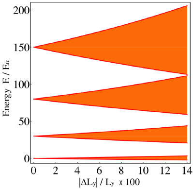
Engineering a long wire with constant width may be, on the other hand, extremely challenging and less relevant for the stability of the topological SC phase. We assume that varies along the wire randomly in atomic–size steps that extend along hundreds of lattice sites in the x–direction, resulting in a function that varies over length scales larger than the width of the wire. These fluctuations generate local variations of the bare sub–band energies given by Eq. (3) of the order of
| (40) |
where is the average width of the nanowire, the value of the local variation, and the lattice spacing. Note that different sub–bands are shifted differently, i.e., the random edge is not equivalent to long-range chemical potential fluctuations. To provide a quantitative measure of this effect, we show in Fig. 16 the evolution of the nanowire sub–bands with the size of the fluctuations . Note that the sub–bands loose their identity in the presence of fluctuations representing a few percent of the wire width, as the broadening becomes comparable with inter–sub-band gaps. The natural question is how this broadening affects the low–energy physics of the nanowire and, in particular, the topological SC phase. Intuition based on the weak–coupling picture would suggest that the topological phase might become unstable, as the parity of the number of sub–bands crossing the chemical potential becomes an ill defined quantity.
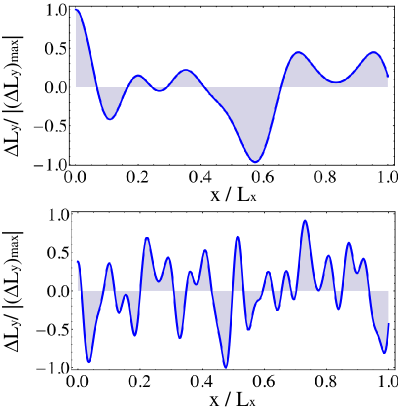
To quantify the effect of random edges on the low–energy physics, we first parametrize this type of disorder. We consider a nanowire of width , where is a random function characterized by by a certain maximum amplitude and a characteristic wavelength. Two examples of random edge profiles are shown in Fig. 17. We note that the actual width of the wire varies in atomic steps, i.e, and we assume that the characteristic length scale of these variations is much larger than the atomic scale. For example, for a nanowire with , a random edge profile like in the upper panel of Fig. 17 and a maximum amplitude of , the atomic edge steps extend over hundreds of unit cells. In the calculations we explore the effect of random edges with maximum amplitudes up to of and various characteristic wavelengths.
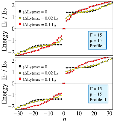
The mini–gap is reduced by the presence of random edges. However, for control parameters corresponding to points in the phase diagram away from phase boundaries, the amplitude of the variations of required for a complete collapse of the gap is well above . Examples of the spectra for systems with random edges are shown in figures 18 and 19. Based on a number of similar calculations for different disorder realizations and control parameters, we have established the following general conclusions:
i) The details of the low–energy spectrum of a disordered nanowire depend on the particular disorder realization. Nonetheless, different disorder profiles characterized by a given amplitude and having the same characteristic length scale are likely to generate similar values of the mini–gap , with the exception of a few “rare events”, which are characterized by significantly lower gap values. A calculation that involves averaging over disorder will capture these “rare events” and will predict a value of the gap much lower than the typical value. Such a calculation would be relevant for an extremely long wire, i.e., in the limit , or for systems with a very large density of states at the relevant energies (e.g., a metal). However, in a typical semiconductor wire the number of states that control the low-energy physics is of the order of . How the energies of these states are modified in the presence of disorder, depends on the specific details of the disorder profile. Hence, any experimentally relevant conclusion regarding the low–energy spectrum or the local density of states of a disordered nanowire should be based on calculations involving specific disorder realizations. A direct consequence of these considerations is that nominally identical samples with the same average disorder (e.g. same mobility) may have very different Majorana minigaps since they are likely to have different disorder configurations. The distribution of the minigaps was recently studied in Ref. Brouwer et al. (2011b).
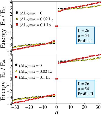
ii) Long range disorder has a stronger effect than short range disorder. This is general characteristic of disordered nanowires, regardless of the source of disorder, and will be studied in more detail in the next section. We note that the effects of variations of wire width at atomic length scales are negligible.
iii) Intermediate coupling represents the optimal SM–SC coupling regime. The large gap that characterizes the topological phase in this regime is robust against fluctuations of the wire width of the order for any set of parameters that are not in the immediate vicinity of a phase boundary. Most importantly, this condition can be satisfied for specific values of the Zeeman field (e.g., of the order for the parameters corresponding to the phase diagram in Fig. 9) over a large range of chemical potentials.
IV.2.2 Nanowires with charged impurities
A major source of disorder in the nanowire consists of charged impurities. Because the carrier density in the SM nanowire is small, charged impurities are not effectively screened and their presence can potentially have significant effects. The nature of these charged impurities, the values of their effective charge and their exact locations depend on the details of the nanowire engineering process and will have to be determined by future experimental studies. Here, we are interested in the fundamental question regarding the stability of the topological SC phase. In particular we address the following question: Is it possible to realize stable zero–energy Majorana modes in a nanowire with charged impurities within a realistic scenario? To answer this general question, we focus on four key aspects of the problem: a) The screening of charged impurities by the electron gas in the SM nanowire, b) The dependence of the low–energy physics on the concentration of impurities, c) The dependence of the low–energy spectrum on the Zeeman field, and d) The effect of long range random potentials.
Screening of charged impurities.
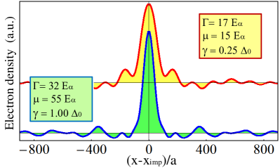
We start by considering a single charge inside or in the vicinity of the nanowire. For concreteness we assume that the charge is positioned near the middle of the wire and one lattice spacing away from its surface, i.e., for a wire that occupies the volume defined by , with , the position of the impurity is given by . This corresponds, for example, to a charged impurity localized at the interface between the SM and the SC. We consider the extreme case , where is the elementary charge, although in practice it is likely that the effective charge is only a fraction of this value due to screening by electrons in the SC. We neglect the screening due to the presence of the superconductor, which may significantly reduce the effective potential created by the charge. A simple estimate of the screening effects due to the electrons in the semiconductor within the Thomas-Fermi approximation is highly inaccurate due to the low carrier density. We checked this property explicitly by calculating numerically the carrier density induced by a given effective potential , e.g., a screened Coulomb potential. We find that the relationship between the induced local carrier density and the local effective potential is highly non-linear. In addition, the density is characterized by strong Friedel–type oscillations (see Fig. 20). Hence, solving quantitatively the screening problem for the nanowire would require a self-consistent calculation that includes electron–electron interactions at the Hartree-Fock level. This calculation is beyond the scope of the present study and will be addressed elsewhere. Here we address a more limited question: What is the characteristic length scale over which the external charge is screened? We define this length scale as the characteristic length of the volume that contains (i.e., a fraction equal to ) of the induced charge.
Specifically, the potential created by the charge at a point inside the semiconductor is
| (41) |
where is the position of the impurity and is the relative dielectric constant of the SM. For InAs . Next, we take into account the fact that the nanowire is extremely thin in the z direction (), hence the wave function profile along this direction is very little affected by the presence of the impurity. On the other hand, the induced charge has a strong dependence on x (the direction along the wire) and y (the transverse direction). As mentioned above, the impurity potential is screened by the induced charge outside a region with a characteristic length scale that contains a fraction equal to of the induced charge. We assume that the screened potential is qualitatively described by an expression of the form
| (42) |
The parameter from Eq. (42) is determined self–consistently by imposing the condition that of the induced charge be in a disk of radius and thickness centered at . The results for two different sets of parameters are shown in Fig. 20. As expected, nanowires with multiple occupied sub–bands provide a more effective screening, which is reflected in a lower value of the screening length . We emphasize that the present approach is not fully self–consistent and is therefore only of qualitative validity. An effective screened potential that includes exactly the contribution of the induced charge with details (e.g., oscillatory components) that are not captured by Eq. (42) should give results very similar to what we obtain here. Nonetheless, we expect these details to have a weak effect on the final results. We also note that the self–consistent calculation of the screening length is done for a non–superconducting nanowire, then the effective impurity potential is added to the total nanowire Hamiltonian before including the proximity effects due to the SM–SC coupling.
What is the effect of the charged impurity on the low-energy spectrum of the superconducting nanowire? The effective potential in the vicinity of the impurity is extremely large, e.g., meV (i.e., ), much larger than any other relevant energy scale in the problem, hence one would naively expect significant effects. However, the low-energy physics of the SM nanowire is controlled by single particle states with low wave numbers and the matrix elements of the impurity potential between these state are relatively small. In other words, the impurity will strongly affect the spectrum at intermediate and high energies, but will have a relatively small effect at low energies. To illustrate this property, we show in Fig. 21 a comparison between the low–energy spectra of a clean nanowire and of a nanowire with a charged impurity. We note that the presence of the external charge induces the formation of localized states in the vicinity of the impurity (see Fig. 21).
Charge impurities in one-dimensional quantum wires produce weakly long-range disorder since the Coulomb potential decays as in the momentum space for with being the short-distance cut-off associated with the transverse dimensions of the nanowire Das Sarma and Lai (1985). This is to be contrasted with the much stronger () long wavelength divergence of the bare Coulomb disorder in two (three) dimensions. The weakly long-range nature of 1D Coulomb potential suggests that any regularization of the long-range disorder would be a reasonable approximation in spite of the fact that Thomas-Fermi screening itself is weak in 1D. In particular, the presence of interband scattering in the multisubband situation would essentially lead to effective 2D screening in the system, which should suffice to regularize the singular Coulomb disorder. At very low densities, where the nanowire is strictly in 1D limit with only the lowest subband occupied, weak screening will lead to the formation of the inhomogeneous electron puddles in the system around the charge impurities due to the failure of screening. This situation is detrimental to the Majorana formation and must be avoided. It is clear that higher density and multisubband occupancy would be favorable for the experimental realization of the Majorana modes in the semiconductor nanowires.
Charged impurity disorder.
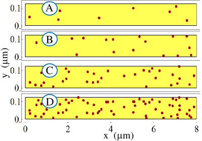
The next question that we address concerns the dependence of the low energy spectrum of a nanowire with charged disorder on the concentration of impurities. We emphasize that the details of the low–energy physics depend on the specific disorder realization. In particular, the low–energy states are localized in the vicinity of the impurities (see Fig. 21) and their energies depend on the specifics of the real–space disorder configuration. Hence, as discussed above, calculations of single-particle quantities, e.g., the local density of states, should involve specific disorder realizations, rather than disorder averaging. In Fig. 22 we show four different specific disorder realizations, corresponding to linear impurity densities ranging from to , which are reasonably realistic impurity densities ( cm-3) in high quality semiconductor structures. The impurities carry charge and are positioned at a distance of one lattice constant away from the SM surface. The effect of these impurities is incorporated through an impurity potential of the form
| (43) |
where is given by Eq. (42) and are the impurity position vectors. We note that in Eq. (43) the screened potential is characterized by a screening length determined as described above for a single impurity. This approximation does not take into account the impact of the dependence of the effective potential associated with a given charged impurity on the location of the charge and on the presence of other impurities. It also neglects the effect of screening by the SC itself which should strongly suppress the effective disorder.
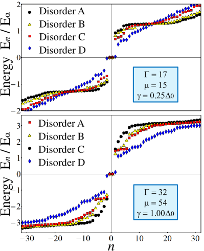
The low–energy spectra of a nanowire with random charged impurities distributed as in Fig. 22 are shown in Fig. 23 for two sets of control parameters. The general trend is that the mini–gap decreases with increasing impurity concentration. However, for a given concentration the exact value of the mini-gap depends on the specific disorder realization. As mentioned above, averaging over disorder includes rare configurations characterized by small mini-gaps, hence the averaged density of states is characterized at low energies by a small weight that does not correspond to any physical state in a typical disorder realization. The signature of a topological SC phase with (i.e., one pair of Majorana fermions) that distinguishes it from the trivial SC phase with is the presence of zero–energy quasiparticles separated by a finite gap from all other excitations. One key conclusion of our calculations is that the mini–gap that protects the topological SC phase remains finite for a significant range of realistic impurity concentrations.
Dependence of the low–energy spectrum on the Zeeman field.
As shown in Fig. 23, for certain high impurity concentrations (e.g., configuration D in fig. 22) it is possible that, in addition to the Majorana zero mode, another low–energy state has energy close to zero and is separated by a gap from the rest of the spectrum. How can one distinguish experimentally this state from a topological superconductor characterized by a finite mini–gap, on one hand, and from a trivial superconductor with , on the other? As the low–energy spectrum has a strong dependence on , the key is to vary the Zeeman field. Tuning may push the system into the topological SC phase and the energy of the additional state will increase. On the contrary, it is possible that varying the Zeeman field will lead to the appearance of more low–energy excitations. This is the characteristic signature of the transition zone between phases with different topologies. To address this problem more systematically, let us consider a nanowire with the same parameters as in the bottom panel of Fig. 10: , , and . The dependence of the quasiparticle gap on for the infinite clean system in shown in Fig. 10, and the dependence of the mini–gap on for a finite wire is shown in Fig. 12. The transition between the trivial SC phase with and the topological phase with is clearly marked by the vanishing of the gap at .
Let us now add disorder and follow the evolution of the lowest three energy levels with the Zeeman field. The results for two different values of the impurity concentration are shown in Fig. 24. First, we note that the main features are similar with those observed in a clean system: at low values of the Zeeman field the system is in a trivial SC phase characterized by finite gap to all excitations, while for above a certain critical value the system has a Majorana zero mode separated by a mini–gap from the rest of the spectrum. The major difference from the clean case consists of the transition zone, which extends over a finite range of values of the Zeeman field and is characterized by multiple low-energy excitations. This transition zone extends with increasing impurity concentration. Assuming that we probe the low-energy properties of the system with a certain finite resolution, e.g., , the topological phase can be unambiguously distinguished from the trivial SC provided the mini–gap is larger that the energy resolution. The trivial phase will be characterized by a finite gap and no zero–energy excitation, while the topological phase will have the characteristic zero–mode separated from the finite energy excitations by the mini–gap. In between the two phases there will be a transition zone characterized, within our finite energy resolution, by a continuum spectrum. Starting with low values of the Zeeman field, i.e., deep inside the phase, by increasing one first reaches the transition zone, the topological phase. We emphasize that for the topological phase becomes indistinguishable from the transition zone. In addition, at large impurity concentrations the mini–gap will collapse completely.
Long range disorder potential.
What is the effect of a long-range disorder potential on the stability of the topological SC phase? Are there qualitative differences from the short–range case discussed above? We are not interested here in the possible source of such long range disorder, but rather in identifying the magnitude of the amplitude of the random potential that would destroy the topological phase.
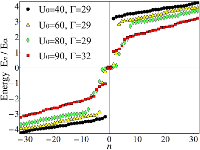
Let us consider a random potential with a characteristic length scale . Neglecting the dependence of the potential on and , we have
| (44) |
where is the amplitude of the potential and is a random profile. For concreteness we consider the profile shown in the lower panel of Fig. 17 and a nanowire with and . These parameters correspond to . The corresponding low–energy spectra for different values of the disorder amplitude are shown in Fig. 25. A striking feature is represented by the significant difference between the critical disorder amplitudes at which the mini–gap collapses for the two slightly different values of the Zeeman field. Note that both values are near the “center” of the topological phase, as one can see, for example, by inspecting the bottom panel of Fig. 12. What sets the scale for the critical amplitude? A hint can be obtained from the phase diagram shown in Fig. 9. In essence, in the presence of a smoothly varying random potential topological superconductivity is stable as long as the local chemical potential at any point within the nanowire has values within the topological phase. The permissible range of variation for the local chemical potential depends strongly on the Zeeman field. From the phase diagram in Fig. 9 and the chemical potential dependence in Fig. 11 it is clear that represents a value of the Zeeman field that allows for large amplitude chemical potential fluctuations.
We conclude that long range disorder can be treated as local chemical potential fluctuations. We emphasize that this is not the case for short range disorder. The topological phase is stable against chemical potential fluctuations up to a maximum amplitude that depends on the Zeeman field, on the average chemical potential, and on the SM–SC coupling. Single band occupancy necessarily limits the critical amplitude due to the close proximity of the phase boundary. Multi–band systems avoid this problem and provide a more efficient screening for the short range potentials created by charged impurities. In addition, a strongly non–uniform coupling between the nanowire and the s–wave SC (with ) with a coupling strength in the intermediate regime () provides the optimal shape of the phase diagram (see Figures 9 and 12).
IV.3 Disorder at the semiconductor–superconductor interface
The inhomogeneous random coupling at the semiconductor–superconductor interface is another significant source of disorder. In principle, the tunneling matrix elements between the nanowire and the s–wave SC are characterized by random real space variations due to inhomogeneities in the tunneling barrier. For example, realizing a nonuniform coupling , which is critical for generating off–diagonal pairing and for stabilizing the topological phase near the sweet spots, may require the growth at the interface of an insulating layer with variable thickness across the wire. Any growth imperfection will translate into variations of . While ultimately the details of these variations will have to be determined by a careful experimental study of the interface, it is reasonable to assume that a typical interface is characterized by atomic size variations with a characteristic length scale of a few lattice spacing, as well as longer range inhomogeneities with characteristic length scales comparable to the width of the wire, , or larger. The short range inhomogeneities could be generated by impurities or by point defects present at the interface, while longer range inhomogeneities could be due to extended defects. In the absence of a detailed microscopic description of the SM–SC interface, it is difficult to estimate the amplitude of these fluctuations. Here we consider a phenomenological model of the interface and we assume that the tunneling matrix is given by
| (45) |
where is the smooth component of the nonuniform coupling, e.g., the interface transparency with the profile shown in Fig. 3, and represents the random component. To model the short range disorder, we coarse grain the interface in square patches of side length and assume that is uniform within a patch, but varies randomly from patch to patch with an amplitude , i.e., with . In the numerical calculations we considered patches of sizes and and an amplitude , where is the maximum value of the smooth nonuniform tunneling component shown in Fig. 3. We note that these are extremely large fluctuations of , larger that the minimum value of the smooth tunneling component, , which result in significant variations of the local effective coupling . Examples of short–range random couplings within the patch model are shown in Fig. 26.
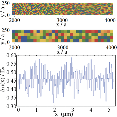
Before we present the results of the numerical calculations, we would like to emphasize the specific way that interface disorder enters the effective Hamiltonian. While the effect of charged impurities can be included through a random potential, variations in the SM-SC coupling generate randomness in the effective SC order parameter, , as well as fluctuations of the renormalization matrix . From equations (25) and (27) we notice that the short range fluctuations of and, implicitly, the short range fluctuations of , are significantly reduced when taking the matrix elements with the eigenstates . As we are mainly interested in systems with only a few occupied sub–bands, integration over effectively averages out fluctuations with characteristic length scales .
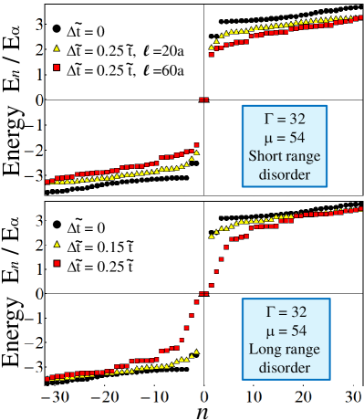
As an illustration of this property, we consider the case of random coupling with and for a nanowire with , , and . In spite of the relatively large length scale of the fluctuation, , the variations of the induced gap along the wire are only of the order of of the average value. The dependence of the induced gap on the position along the wire is shown in the lower panel of Fig. 20. The amplitude of the fluctuations is further reduced if we consider shorter range coupling fluctuations. A similar behavior characterizes the renormalization matrix . In addition, as the low–energy properties of the system are determined by single particle states with small wave vectors , we expect a further reduction of the effect of short range fluctuations as a result of the integration over . In particular, if the clean, infinite wire is characterized by a maximum Fermi wave vector , we expect the low-energy physics to be insensitive to random variations of the SM–SC coupling with characteristic length–scales .
The effects of a random SM–SC coupling on the low–energy spectrum of the nanowire are illustrated in Fig. 27. Remarkably, short range fluctuations with amplitudes up to of the average coupling at (i.e., the maximum value of the coupling in a nonuniform profile - see Fig. 3) do not destroy the topological SC phase. The relatively weak effect of these strong fluctuations is due to the implicit averaging involved in the calculation of the matrix elements between single particle states with low wave vectors. Increasing the characteristic length makes this type of disorder more effective, as evident from the upper panel of Fig. 27. Hence the natural question: what is the effect of long–range SM–SC coupling fluctuations? We consider a smooth variation of along the wire with a profile as shown in the upper panel of Fig. 17. An amplitude of these fluctuations equal to of results in the collapse of the gap (see Fig. 27, lower panel). However, the topological phase is robust against long range coupling fluctuations with amplitudes smaller than . We note that long range variations of the coupling strength could result from the engineering process of the nonuniform interface. Limiting the amplitude of these fluctuations below a certain limit of about of the maximum coupling strength should be a priority of the experimental effort for realizing a topological SC state using semiconductor nanowires.
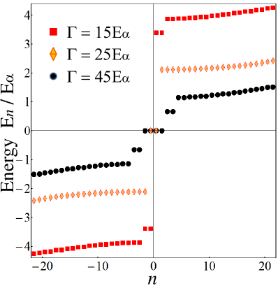
V Experimental signatures of Majorana bound states
Probing unambiguously the presence of Majorana bound states in the superconducting nanowire represents a critical task. In this section we show that local spectral measurements provide a simple and effective tool for accomplishing this task. We focus on the local density of states (LDOS), which could be measured using, for example, scanning tunneling spectroscopy (STS), and on the differential conductance associated with tunneling into the ends of the wire. We establish that these measurements should suffice in establishing the existence of the zero-energy Majorana edge modes in semiconductor nanowires.
V.1 Local density of states in superconducting nanowires
In the previous section we have shown that disorder generates low–energy states and reduces the mini–gap. Nonetheless, a small mini–gap does not implicitly mean that the Majorana bound state cannot be resolved in a spectroscopic measurement. The key observation is that the undesirable low–energy states are generally localized near impurities and defects (see, foe example, Fig. 21). A local measurement could easily distinguish between a zero–energy state localized at the end of the wire and a low–energy state localized somewhere inside the wire. To clarify the question regarding the real space distribution of the low–energy spectral weight, we calculate the local density of states (LDOS) for several relevant regimes and compare the LDOS of a clean ideal system with that of a disordered realistic nanowire.
We start with a clean nanowire with three occupied sub–bands ( ) coupled non–uniformly to an s-wave superconductor. The coupling parameter is characterized by a non–homogeneity factor and an intermediate coupling strength , where is the SC order parameter of the superconductor. In the absence of a Zeeman field (), the nanowire is a trivial superconductor. Increasing the Zeeman field above a critical value induces a transition from the trivial SC phase with (no Majorana modes) to a topological SC phase with (one pair of Majorana modes). Further increasing drives the system though a series of alternating phases with trivial ( even) and non-trivial ( odd) topologies (see the phase diagram in Fig. 9). Of major practical interest are the first two phases ( and ), as stronger Zeeman fields involve smaller gaps (see Fig. 10) or may destroy superconductivity altogether. Typical spectra from the first three phases () are shown in Fig. 28 and the corresponding LDOS is shown in Fig. 29.
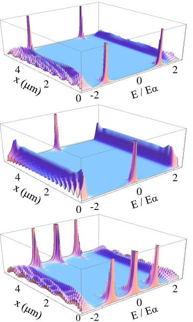
The main conclusion suggested by the results shown in Fig. 29 is that clear–cut evidence for the existence of the Majorana zero modes can be obtained by driving the system from a trivial SC phase with to a topological SC state with by tuning the Zeeman field. In the trivial SC phase there is a well–defined gap for all excitations, including states localized near the ends of the wire. By contrast, the topological SC phase is characterized by sharp zero–energy peaks localized near the ends of the wire and separated from all other excitations (including possible localized in–gap states) by a well–defined mini–gap.
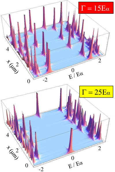
Is it possible to clearly distinguish the two phases with different topologies in the presence of disorder? The answer is provided by the results shown in Fig. 30 for a nanowire with charged impurities. In contrast with the clean case, all the low-energy states are strongly localized. Nonetheless, the signature features of the two phases (the gaps and the zero–energy peaks) are preserved. At this point we emphasize two critical properties:
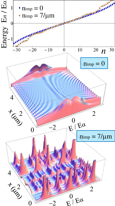
i) The features illustrated in Fig. 30 are generic, i.e., they do not depend on the type or the source of disorder. Similar LDOS can be generated using any other significant type of disorder discussed in the previous section, or combinations of different types of disorder. ii) Observing a zero–energy peak at a certain value of the Zeeman field does not by itself prove the realization of a topological SC phase. The trivial SC state with may also have a zero–energy peak separated from all other excitations by a mini-gap. To clearly identify the phase one must measure the LDOS as a function of the Zeeman field starting from , i.e., from the trivial SC phase with . Continuously increasing will generate a transition from a phase characterized by a well–defined gap to a phase with strong zero–energy peaks localized near the ends of the wire. But what is the signature of the transition?
Figure 31 shows the spectrum and the LDOS of a system with a Zeeman field . In a clean wire this corresponds to the transition between the and phases, which is marked by the vanishing of the quasi–particle gap, as shown in figures 10 and 12. The LDOS is characterized by a distribution of the spectral weight over the entire low–energy range of interest. This property holds at any position along the wire. Adding disorder induces localization, but does not change this key property. In fact, based on the analysis of the results shown in Fig. 24, we know that in disordered systems this type of critical behavior will characterize a finite range of Zeeman fields. Observing the transition between the topologically trivial and nontrivial phases, which is characterized by the closing of the gap and by a spectral weight distributed over a wide energy range, is the final ingredient necessary for unambiguously identifying the Majorana bound states using LDOS measurements.
V.2 Tunneling differential conductance
An ideal type of measurement that exploits the properties identified in the previous subsection consists of tunneling into the ends of the wire and measuring the differential conductance Yamashiro_PRB'97 ; Bolech_PRL'08 ; Tewari_PRL'08 ; Nilsson_PRL'08 ; Law_PRL'09 . To a first approximation, is proportional to the local density of states at the end of the wire, so the general discussion presented above should apply. Here, we focus on certain specific aspects of a tunneling experiment, e.g., the specific form of the tunneling matrix elements and the role of finite temperature, that may limit the applicability of our conclusions. We find that values of the parameters consistent with an unambiguous identification of the Majorana bound state in the semiconductor nanowire are well within a realistic parameter regime.
The tunneling current between a metallic tip and the nanowire can be evaluated within the Keldysh non-equilibrium formalism Berthod and Giamarchi (2011). In terms of real space Green’s functions we have
| (46) | ||||
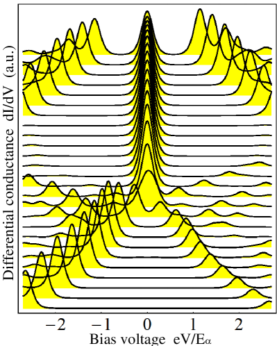
where is the bias voltage applied between the tip and the nanowire and is the Fermi-Dirac distribution function corresponding to a temperature . The retarded (advanced) Green’s function for the nanowire has the expression
| (47) |
where and are the particle and hole components of the wave function corresponding to the energy . The wave functions and the energies are obtained by diagonalizing the effective BdG Hamiltonian for the nanowire, including the contibution from disorder, as described in the previous sections. The matrices contain information about the tip and the tip–nanowire coupling. Specifically, we have
| (48) |
where represents the density of states of the metallic tip and depends on the tunneling matrix elements between the tip and the wire. We note that in Eq. (46) the trace is taken over the position vectors. We consider a tunneling model in which the amplitude of the tunneling matrix elements vary exponentially with the distance from the metallic tip. Specifically, we have , where gives the overall strength of the tip–nanowire coupling and the position–dependent factor is
| (49) |
with being the position vector for the tip and a characteristic length scale associated with the exponential decay of the tip–wire coupling. In the numerical calculations we take and , i.e., the tip is is at a distance equal with three lattice spacings away from the end of the wire. With these choices, the differential conductance becomes
| (50) |
where the matrix elements and involve summations over the lattice sites of the nanowire system and provide the amplitudes for tunneling into specific states. Finite temperature effects are incorporated through the derivatives of the Fermi–Dirac function, .
The dependence of the tunneling differential conductance on the bias voltage for a superconducting nanowire with disorder is shown in Fig. 32. Different curves correspond to different values of the Zeeman field between (bottom) and (top) and are shifted vertically for clarity. The temperature used in the calculation is , a value that can be easily reached experimentally. Lower temperature values will generate sharper features, but the overall picture remains qualitatively the same. Note that the closing of the gap in the critical region between the trivial SC phase and the topological SC phase can be clearly observed. In this region has features over the entire low-energy range, as discussed in the previous subsection. The Majorana bound state at is clearly marked by a sharp peak at , separated by a gap from other finite energy features. We conclude that measuring the tunneling differential conductance can provide a clear and unambiguous probe for Majorana bound states in semiconductor nanowires.
VI Conclusions
In conclusion, we have developed a comprehensive theory for the realization and the observation of the emergent non-Abelian Majorana mode in semiconductor (e.g., InAs, InSb) nanowires proximity coupled to an ordinary s–wave superconductor (e.g., Al, Nb) in the presence of a Zeeman splitting induced by an external magnetic field. The importance of our work lies in the thorough investigation of the experimental parameter space, which is required in order to predict the optimal parameter regime to search for the Majorana mode in nanowires. Since the number of possible physical parameters in the problem is large (e.g., electron density in the nanowire, geometric size of the wire, chemical potential, the strength of spin-orbit coupling, the superconducting gap, the hopping matrix elements between the semiconductor and the superconductor, the strengths of various disorder in the semiconductor, or in the superconductor, or at the interface between them), theoretical guidance, as provided in this work, is highly desirable for the success of the experimental search for the Majorana fermion in solid–state systems. Aside from the obvious conclusions (e.g., strong spin-orbit coupling and large Lande -factor in the semiconductor, large superconducting gap in the superconductor, and low disorder everywhere stabilize the topological phase), we have discovered several unexpected results. In particular, we find somewhat surprisingly that the strict one-dimensional limit with purely one–subband occupancy for the nanowire, as originally envisioned by Kitaev Kitaev (2001) and later used by many researchers Lutchyn et al. (2010); Oreg et al. (2010); Alicea et al. (2011), is not only unnecessary, but is in fact detrimental to creating Majorana modes. In the presence of disorder, the optimal system should have a few ( 3-5) occupied subbands in the nanowire for the creation of the Majorana modes with maximal stability. This is, of course, great news from the experimental perspective, because fabricating strictly 1D semiconductor nanowires with pure one subband occupancy is a challenging task. Another important result of our analysis is the relative immunity of the Majorana modes to the presence of disorder in the system. The most dangerous disorder mechanisms are due to charged impurity centers in the semiconductor and to inhomogeneous hopping across the semiconductor-superconductor interface. Our work suggests that the optimal nanowires for observing the Majorana mode should not only have as little charge impurity disorder as possible in the semiconductor, but they should also have a thin insulating layer separating the semiconductor and superconductor (so that the tunneling across the interface is not too strong), as well as some non–uniformity in the tunneling amplitude between the semiconductor and the superconductor across the width (but not the length) of the nanowire. Our detailed numerical calculations establish that the zero–energy Majorana modes should clearly show up in experiments, even in the presence of considerable disorder in the nanowires. In addition, we establish that the disorder in the superconductor has little effect on the Majorana mode in the nanowire. Another salient aspect of our work is the detailed calculation of the expected tunneling spectroscopy spectra for observing the Majorana mode in the nanowire using realistic physical parameters. Our results establish that the predicted topological quantum phase transition between the trivial phase with no Majorana mode to the topological phase with a well-defined zero energy Majorana bound state should be clearly observable as a striking zero-bias anomaly in the tunneling current when the Zeeman splitting is tuned through the quantum critical point separating the two phases. More importantly, we calculate realistic tunneling spectra in the presence of uncontrolled spurious bound states in the system which are invariably present in real samples due to the localized random impurities in the semiconductor environment, clearly showing how to discern the topological features associated with the Majorana bound states from the background of contributions due to trivial bound states caused by impurities in the system.
Our work emphasizes the tunneling measurements, which would directly establish the existence of a robust zero energy mode in the system, providing the necessary condition for the existence of the Majorana fermion. What we have done here is to develop a detailed theory for the existence of a topological phase in the semiconductor-superconductor heterostructure, by taking into account essentially all of the relevant physical effects. Once the presence of a robust zero energy mode is established, hence the necessary condition for the existence of the Majorana is realized, one must move on to establish the sufficient condition, which would obviously be a harder task. Several ideas for establishing definitively the existence of the Majorana mode (and its non-Abelian braiding statistics nature) have already been suggested in the literature, including experiments involving the fractional Josephson effect Lutchyn et al. (2010); Kitaev (2001); Fu and Kane (2009); Yakovenko'03 ; Alicea et al. (2011), the quantized differential conductance Law_PRL'09 ; Wimmer'11 , and Majorana interferometry FuKanePRL'11 ; Akhmerov_prl'09 ; Sau_prb'11 .
Our work establishes the realistic likelihood of the existence within laboratory conditions of the non-Abelian Majorana zero–energy mode in spin–orbit interacting semiconductor nanowires proximity–coupled to ordinary superconductors. We also establish that tunneling spectroscopy is one of the easiest techniques to directly observe the elusive Majorana in realistic solid–state systems. Greater challenges, such as carrying out topological quantum computation, lie ahead once the laboratory existence of the Majorana mode is established experimentally.
Acknowledgements.
We would like to thank Leonid Glazman, Matthew Fisher and Chetan Nayak for discussions. This work is supported by the DARPA QuEST, JQI-NSF-PFC, Microsoft Q (SDS) and WVU startup funds (TS).References
- Wilczek (2009) F. Wilczek, NATURE PHYSICS 5, 614 (2009).
- Stern (2010) A. Stern, Nature 464, 187 (2010).
- Franz (2010) M. Franz, Physics 3, 24 (2010).
- Nayak (2010) C. Nayak, Nature 464, 693 (2010).
- Majorana (1937) E. Majorana, Il Nuovo Cimento (1924-1942) 14, 171 (1937).
- Levi (2011) B. G. Levi, Physics Today 64, 20 (2011).
- Service (2011) R. F. Service, Science 332, 193 (2011).
- Nayak and Wilczek (1996) C. Nayak and F. Wilczek, Nucl. Phys. B 479, 529 (1996).
- Read and Green (2000) N. Read and D. Green, Phys. Rev. B 61, 10267 (2000).
- Ivanov (2001) D. A. Ivanov, Phys. Rev. Lett. 86, 268 (2001).
- Kitaev (2001) A. Y. Kitaev, Physics-Uspekhi 44, 131 (2001), eprint cond-mat/0010440.
- Stern et al. (2004) A. Stern, F. von Oppen, and E. Mariani, Phys. Rev. B 70, 205338 (2004).
- Nayak et al. (2008) C. Nayak, S. H. Simon, A. Stern, M. Freedman, and S. Das Sarma, Rev. Mod. Phys. 80, 1083 (2008), eprint arXiv:0707.1889.
- Alicea et al. (2011) J. Alicea, Y. Oreg, G. Refael, F. von Oppen, and M. P. A. Fisher, Nature Physics 7, 412 (2011), eprint 1006.4395.
- Kitaev (2003) A. Y. Kitaev, Ann. Phys.(N.Y.) 303, 2 (2003).
- Das Sarma et al. (2005) S. Das Sarma, M. Freedman, and C. Nayak, Phys. Rev. Lett. 94, 166802 (2005).
- Stern and Halperin (2006) A. Stern and B. I. Halperin, Phys. Rev. Lett. 96, 016802 (2006), eprint cond-mat/0508447.
- Bonderson et al. (2006) P. Bonderson, A. Kitaev, and K. Shtengel, Phys. Rev. Lett. 96, 016803 (2006), eprint cond-mat/0508616.
- Bravyi (2006) S. Bravyi, Phys. Rev. A 73, 042313 (2006).
- Tewari et al. (2008) S. Tewari, C. Zhang, S. Das Sarma, C. Nayak, and D.-H. Lee, Phys. Rev. Lett. 100, 027001 (2008).
- Bonderson et al. (2010) P. Bonderson, D. J. Clarke, C. Nayak, and K. Shtengel, Phys. Rev. Lett. 104, 180505 (2010), eprint arXiv:0911.2691.
- Hassler et al. (2010) F. Hassler, A. R. Akhmerov, C.-Y. Hou, and C. W. J. Beenakker, New Journal of Physics 12, 125002 (2010).
- Sau et al. (2010) J. D. Sau, S. Tewari, and S. Das Sarma (2010), eprint arXiv:1007.4204.
- Bonderson and Lutchyn (2011) P. Bonderson and R. M. Lutchyn, Phys. Rev. Lett. 106, 130505 (2011).
- Clarke et al. (2010) D. J. Clarke, J. D. Sau, and S. Tewari, ArXiv e-prints (2010), eprint 1012.0296.
- Flensberg (2011) K. Flensberg, Phys. Rev. Lett. 106, 090503 (2011).
- Hassler et al. (2011) F. Hassler, A. R. Akhmerov, and C. W. J. Beenakker, ArXiv e-prints (2011), eprint 1105.0315.
- Jiang et al. (2011) L. Jiang, C. L. Kane, and J. Preskill, Phys. Rev. Lett. 106, 130504 (2011).
- (29) O. Zilberberg, B. Braunecker, and D. Loss, Phys. Rev. A 77, 012327 (2008)
- Fu and Kane (2008) L. Fu and C. L. Kane, Phys. Rev. Lett. 100, 096407 (2008), eprint arXiv:0707.1692.
- Sau et al. (2010a) J. D. Sau, R. M. Lutchyn, S. Tewari, and S. Das Sarma, Phys. Rev. Lett. 104, 040502 (2010a).
- Das Sarma et al. (2006) S. Das Sarma, C. Nayak, and S. Tewari, Phys. Rev. B 73, 220502 (2006).
- Fu and Kane (2009) L. Fu and C. L. Kane, Phys. Rev. B 79, 161408 (2009).
- Wimmer et al. (2010) M. Wimmer, A. R. Akhmerov, M. V. Medvedyeva, J. Tworzydło, and C. W. J. Beenakker, Phys. Rev. Lett. 105, 046803 (2010).
- Lee (2009) P. A. Lee, ArXiv e-prints (2009), eprint 0907.2681.
- Alicea (2010) J. Alicea, Phys. Rev. B 81, 125318 (2010).
- Lutchyn et al. (2010) R. M. Lutchyn, J. D. Sau, and S. Das Sarma, Phys. Rev. Lett. 105, 077001 (2010), eprint arXiv:1002.4033.
- Oreg et al. (2010) Y. Oreg, G. Refael, and F. von Oppen, Phys. Rev. Lett. 105, 177002 (2010).
- Sau et al. (2010b) J. D. Sau, S. Tewari, R. M. Lutchyn, T. D. Stanescu, and S. Das Sarma, Phys. Rev. B 82, 214509 (2010b).
- Lutchyn et al. (2011) R. M. Lutchyn, T. D. Stanescu, and S. Das Sarma, Phys. Rev. Lett. 106, 127001 (2011).
- Mao et al. (2011) L. Mao, M. Gong, E. Dumitrescu, S. Tewari, and C. Zhang, ArXiv e-prints (2011), eprint 1105.3483.
- Potter and Lee (2010) A. C. Potter and P. A. Lee, Physical Review Letters 105, 227003 (2010), eprint 1007.4569.
- Potter and Lee (2011) A. C. Potter and P. A. Lee, Phys. Rev. B 83, 094525 (2011), eprint 1011.6371.
- Qi et al. (2010) X.-L. Qi, T. L. Hughes, and S.-C. Zhang, Phys. Rev. B 82, 184516 (2010).
- (45) J. Linder, Y. Tanaka, T. Yokoyama, A. Sudbo, and N. Nagaosa, Phys. Rev. Lett. 104, 067001 (2010)
- Nadj-Perge et al. (2010) S. Nadj-Perge, S. M. Frolov, E. P. A. M. Bakkers, and L. P. Kouwenhoven, NATURE 468, 1084 (2010).
- Nilsson et al. (2009) H. A. Nilsson, P. Caroff, C. Thelander, M. Larsson, J. B. Wagner, L.-E. Wernersson, L. Samuelson, and H. Q. Xu, Nano Letters 9, 3151 (2009).
- Aleshkin et al. (2008) V. Aleshkin, V. Gavrilenko, A. Ikonnikov, S. Krishtopenko, Y. Sadofyev, and K. Spirin, Semiconductors 42, 828 (2008), ISSN 1063-7826.
- (49) Y.-J. Doh, J. van Dam, A. Roest, E. Bakkers, L. Kouwenhoven, and S. D. Franceschi, Science 309, 272 (2005).
- (50) J. A. van Dam, Y. V. Nazarov, E. P. A. M. Bakkers, S. D. Franceschi, and L. P. Kouwenhoven, Nature 442, 667 (2006).
- Chrestin et al. (1997) A. Chrestin, T. Matsuyama, and U. Merkt, Phys. Rev. B 55, 8457 (1997).
- Lutchyn and Fisher (2011) R. M. Lutchyn and M. P. A. Fisher, ArXiv e-prints (2011), eprint 1104.2358.
- DE GENNES (1964) P. G. de Gennes, Rev. Mod. Phys. 36, 225 (1964).
- Alexandrov and Kabanov (2008) A. S. Alexandrov and V. V. Kabanov, Phys. Rev. B 78, 132510 (2008).
- McMillan (1968) W. L. McMillan, Phys. Rev. 175, 537 (1968).
- Gangadharaiah et al. (2011) S. Gangadharaiah, B. Braunecker, P. Simon, and D. Loss, ArXiv e-prints (2011), eprint 1101.0094.
- Sela et al. (2011) E. Sela, A. Altland, and A. Rosch, ArXiv e-prints (2011), eprint 1103.4969.
- Stoudenmire et al. (2011) E. M. Stoudenmire, J. Alicea, O. A. Starykh, and M. P. A. Fisher, ArXiv e-prints (2011), eprint 1104.5493.
- Sau et al. (2010c) J. D. Sau, S. Tewari, R. M. Lutchyn, T. D. Stanescu, and S. Das Sarma, Phys. Rev. B 82, 214509 (2010c).
- Stanescu et al. (2010) T. D. Stanescu, J. D. Sau, R. M. Lutchyn, and S. Das Sarma, Phys. Rev. B 81, 241310 (2010).
- Ghosh et al. (2010) P. Ghosh, J. D. Sau, S. Tewari, and S. Das Sarma, Phys. Rev. B 82, 184525 (2010).
- Akhmerov et al. (2011) A. R. Akhmerov, J. P. Dahlhaus, F. Hassler, M. Wimmer, and C. W. J. Beenakker, Phys. Rev. Lett. 106, 057001 (2011).
- Beenakker et al. (2011) C. W. J. Beenakker, J. P. Dahlhaus, M. Wimmer, and A. R. Akhmerov, Phys. Rev. B 83, 085413 (2011).
- Abrikosov and Gor’kov (1961) A. A. Abrikosov and L. P. Gor’kov, Soviet Phys. JETP 12, 1243 (1961).
- (65) A. C. Potter and P. A. Lee, Phys. Rev. B 84, 059906(E) (2011); R.M. Lutchyn, T. Stanescu and S. Das Sarma, arXiv:1110.5643 (2011).
- Tewari et al. (2011) S. Tewari, T. D. Stanescu, J. D. Sau, and S. D. Sarma, New Journal of Physics 13, 065004 (2011).
- Motrunich et al. (2001) O. Motrunich, K. Damle, and D. A. Huse, Phys. Rev. B 63, 224204 (2001).
- Gruzberg et al. (2005) I. A. Gruzberg, N. Read, and S. Vishveshwara, Phys. Rev. B 71, 245124 (2005).
- Brouwer et al. (2011a) P. W. Brouwer, M. Duckheim, A. Romito, and F. von Oppen, ArXiv e-prints (2011a), eprint 1103.2746.
- Brouwer et al. (2011b) P. W. Brouwer, M. Duckheim, A. Romito, and F. von Oppen, ArXiv e-prints (2011b), eprint 1104.1531.
- Das Sarma and Lai (1985) S. Das Sarma and W.-Y. Lai, Phys. Rev. B 32, 1401 (1985).
- (72) M. Yamashiro, Y. Tanaka, and S. Kashiwaya, Phys. Rev. B 56, 7847 (1997)
- (73) C. J. Bolech and E. Demler, Phys. Rev. Lett. 98, 237002 (2007)
- (74) S. Tewari, C. Zhang, S. Das Sarma, C. Nayak, and D.-H. Lee, Phys. Rev. Lett. 100, 027001 (2008)
- (75) J. Nilsson, A. R. Akhmerov, and C. W. J. Beenakker, Phys. Rev. Lett. 101, 120403 (2008)
- (76) K. T. Law, P. A. Lee, and T. K. Ng, Phys. Rev. Lett. 103, 237001 (2009)
- Berthod and Giamarchi (2011) C. Berthod and T. Giamarchi, ArXiv e-prints (2011), eprint 1102.3895.
- (78) H. J. Kwon, K. Sengupta, and V. M. Yakovenko, Eur. Phys. J. B 37, 349 (2003).
- (79) M. Wimmer, A.R. Akhmerov, J.P. Dahlhaus, C.W.J. Beenakker, New J. Phys. 13, 053016 (2011)
- (80) L. Fu and C. L. Kane , Phys. Rev. Lett. 102, 216403 (2009)
- (81) A. R. Akhmerov, J. Nilsson, and C. W. J. Beenakker, Phys. Rev. Lett. 102, 216404 (2009)
- (82) J. D. Sau, S. Tewari, and S. Das Sarma, Phys. Rev. B 84, 085109 (2011)