Strain effects on the thermal properties of ultra-scaled Si nanowires
Abstract
The impact of uniaxial and hydrostatic stress on the ballistic thermal conductance () and the specific heat () of [100] and [110] Si nanowires are explored using a Modified Valence Force Field phonon model. An anisotropic behavior of and isotropic nature of under strain are predicted for the two wire orientations. Compressive (tensile) strain decreases (increases) . The trend with strain is controlled by the high energy phonon sub-bands. Dominant contribution of the low/mid (low/high) energy bands in [100] ([110]) wire and their variation under strain governs the behavior of .
The wide application of Silicon nanowires (SiNWs) in areas ranging from Complementary-Metal-Oxide-Semiconductor (CMOS) transistors Sinwfet ; sinwfet2 to thermoelectric (TE) devices Hochbaum2008 , non-volatile memories sinw_nvm and, solar cells sinw_solar_cells has made SiNWs an extremely useful nano-electronics device concept. Device properties can be engineered sinw_electron_strain_1 ; sinw_electron_strain_2 through the introduction of built-in stress by process engineering and by external forces like wafer bending strain_size_sinw . Tuning thermal properties using strain can be beneficial for cooling and increasing gain of lasers strain_size_sinw ; strain_effect_1 or improving the efficiency of TE devices strain_effect_1 .
Prior Work: Strain/stress effects on the thermal conductivity of doped bulk zinc-blende (ZB) semiconductors at low temperatures has been well studied phonon_uniax ; Stress_phonon_GaAs . Most of the bulk studies in ZB semiconductors found decrease in thermal conductivity with tensile strain which is qualitatively attributed to (i) a decrease in the phonon mean free path thermal_inc_quality , (ii) an increase in the Debye temperature strain_size_sinw ; thermal_inc_quality , and (iii) a change in the material stiffness shape_depend_theory . The few experimental sige_strain_measure and theoretical strain_size_sinw ; strain_effect_1 ; strain_effect_2 ; shape_depend_theory efforts that have focused on the strain effects on the thermal properties in nanostructures, are either limited to single crystal orientation (mostly [100]) or diffusive phonon transport even in small nanostructures. This work investigates the external strain effects on the thermal properties in ultra-scaled SiNWs in the coherent phonon transport regime where the wire cross-section sizes are comparable to the phonon wavelengths coherent_phonon ( at = 6.5 km/sec for a 3nm X 3nm [100] SiNW vff_iwce_paper , where and h are the Boltzmann constant and Planck’s constant, respectively).
Free-standing SiNWs’ phonon dispersion are studied using the modified valence force (MVFF) model VFF_mod_herman ; vff_own_paper ; vff_iwce_paper . The MVFF model has been shown to correctly reproduce the strain effects like the Gruneisen parameters VFF_mod_herman ; vff_own_paper and third order elastic constants in bulk Si and Ge VFF_mod_herman . The same set of Si MVFF parameters VFF_mod_herman ; vff_own_paper are used in this work to model the SiNW phonon dispersion under hydrostatic and uniaxial stress.
The ballistic thermal conductance () across a semiconductor wire maintained under a small temperature gradient , can be calculated from the calculated phonon dispersion, using the Landauer’s formula Land using Eq.(1) jauho_method ; mingo_ph ,
| (1) |
| (2) |
where N is the number of energy bins in the entire phonon dispersion energy range.The terms , M(E), T, and are the strain percentage, the number of modes at phonon energy E, the temperature, and the electronic charge, respectively. The term is the contribution to the total of SiNW for E . This energy resolved representation in Eq. (1) allows for better understanding of the variation in due to strain.
From the calculated phonon dispersion the constant volume specific heat () at a given T, can be calculated Fph_1 as,
| (3) |
where is the mass of the SiNW unitcell in kg. The quantity is the phonon eigen energy associated with the branch ‘n’ and crystal momentum vector ‘q’.
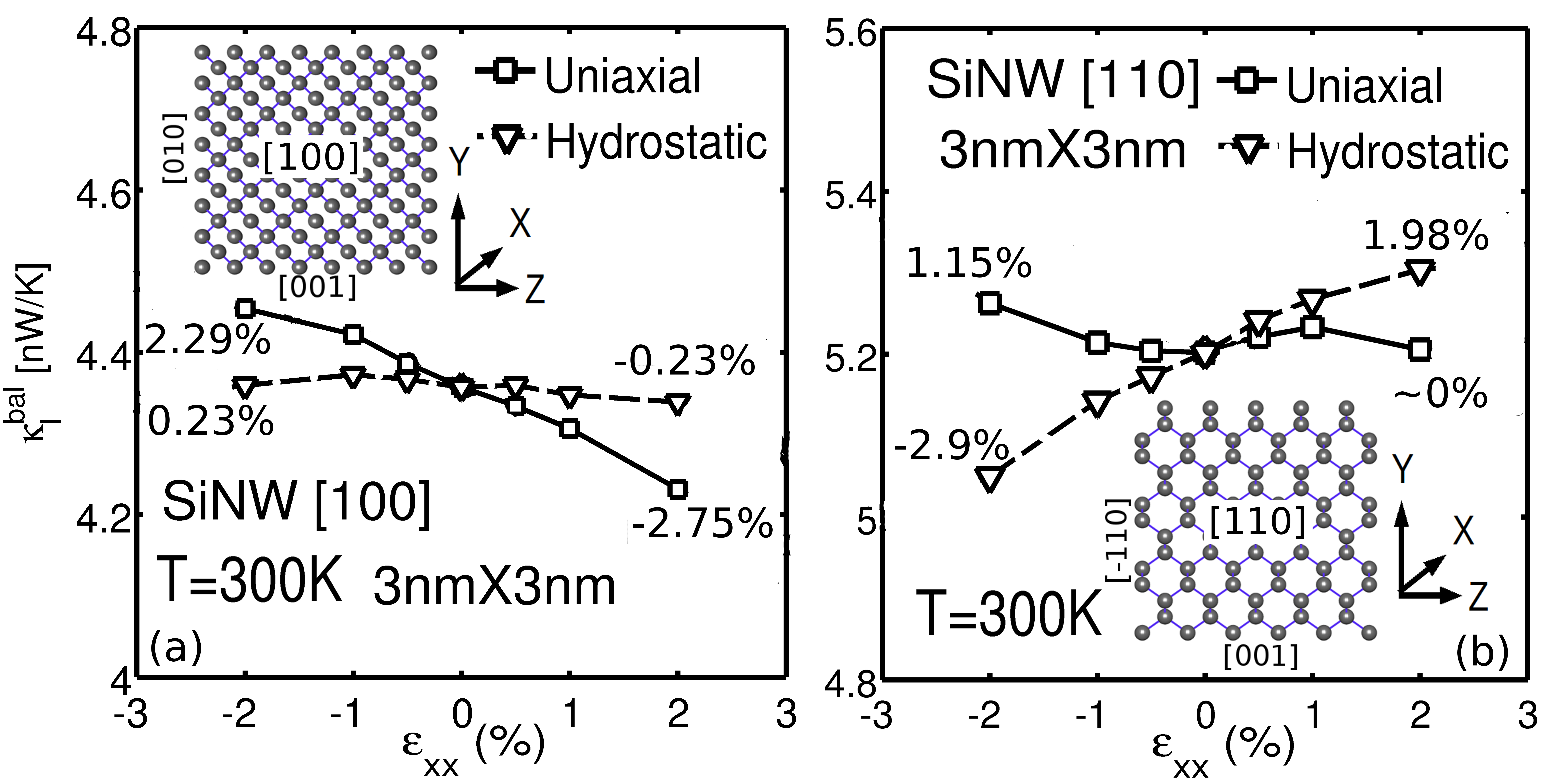
SiNW details: Square NWs with width (W) and height (H) = 3nm with two channel orientations of 100 and 110 are studied (inset of Fig. 1a,b). Hydrostatic deformation (equal deformation along all the directions) and uniaxial deformation (along the wire axis) are applied to these wires varying up to 2%. The outer surface atoms in these NWs are allowed to vibrate freely. Extremely small SiNWs may show significant surface and internal atomic reconstruction Amrit ; strain_effect_1 or phase change strain_effect_1 under strain leading to larger changes in and , are outside the scope of the present study.
Ballistic thermal conductance : In all the SiNWs is calculated using Eq.(1) at 300K. increases (decreases) under uniaxial compression (tension) for both the wire orientations. Similar variations in for [100] SiNWs are also observed by Li. et alstrain_effect_1 using non-equilibrium molecular dynamics (NEMD) calculations. The [100] SiNW shows larger variation in under tensile uniaxial deformation compared to the [110] SiNW (Fig. 1a,b). shows a weak hydrostatic stress dependence in [100] SiNW in contrast to the [110] SiNW which shows a decrease (increase) of 2.9% (1.98%) in under 2% compressive (tensile) strain from the unstrained value (Fig. 1a,b). Similar strain behavior is obtained in SiNWs with W=H up to 5nm, which are not shown here for the sake of brevity. Thus, ultra-scaled SiNWs show an anisotropic variation in under hydrostatic deformation.
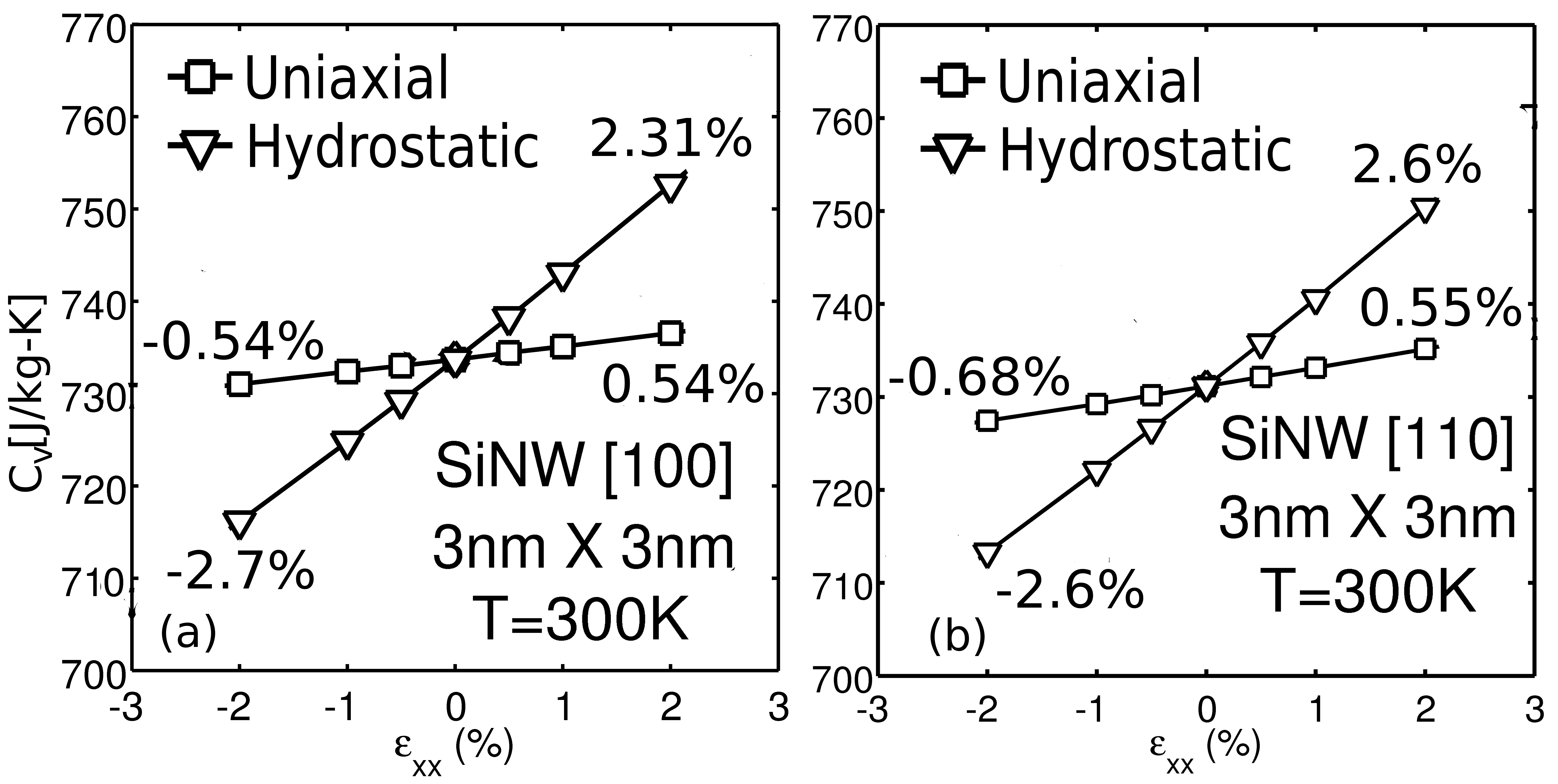
Specific heat (): Variation in the phonon dispersion under strain also changes the of SiNWs. Compressive (tensile) strain decreases (increases) the in both types of SiNWs (Fig. 2a,b)). This variation in is similar to the bulk Si behavior as reported in Refs.strain_effect_2 ; shape_depend_theory . Under hydrostatic stress the decreases by at 2% compression and increases to at 2% expansion compared to the unstrained value for both the SiNW orientations. Under uniaxial deformation the variation is for 2% strain for both wire orientations (Fig. 2a,b). Hence, variation is isotropic under strain in ultra-scaled SiNWs.
| Strain, [Or] | Dom. | Cm to | |||
|---|---|---|---|---|---|
| (meV) | (0-22) | (22-44) | (44-65) | band | Tn |
| U, [100] | 36%-34% | 52%-50% | 13%-13% | L,M | |
| H, [100] | 32%-37% | 56%-45% | 11%-16% | M | |
| U, [110] | 49%-46% | 42%-46% | 10%-8% | L,H | |
| H, [110] | 45%-48% | 45%-44% | 7%-10% | L,H |
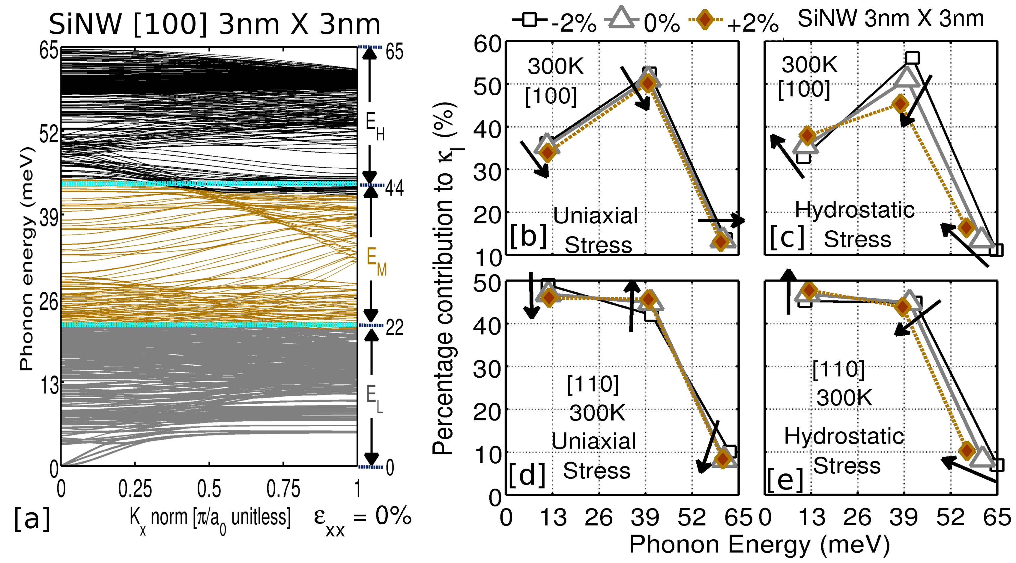
Reason for the variation in : To understand the variation in with strain, the energy dependent contributions are analyzed using Eq. (1). The entire phonon spectrum is grouped into three energy ranges, (i) (‘low’ bands), (ii) (‘mid’ bands) and, (iii) (‘high’ bands) (see Fig. 3 a). These bands show variable contributions under strain which determine the overall effect on (Table 1).
Under uniaxial strain, in [100] SiNW contribution to is mainly from , which decreases from 88% under compression (Cm) to 84% under tension (Tn) (Fig. 3b), whereas in [110] SiNW the contribution to is mainly from , which reduces from 59% (Cm) to 54% (Tn) (Fig. 3d). Under hydrostatic strain, in [100] SiNW main contribution to is from , which reduces from 56% (Cm) to 45% (Tn) (Fig. 3c), while in [110] SiNW main contribution to is from , which increases from 52% (Cm) to 58% (Fig. 3e). These details are also summarized in Table 1. Thus, low/mid energy contribution for [100] SiNW and low/high energy contribution for [110] SiNW explains the anisotropic nature of .
Reason for variation: Under the action of strain the contribution of the phonon bands in range varies considerably as shown in Fig. 4. Under uniaxial stress, both [100] and [110] SiNWs show almost no variation in the and range, and minute variation in the range(Fig. 4a,c). The contribution increases from Cm to Tn in the range which governs the trend under uniaxial strain (Fig. 2). Under hydrostatic stress, contribution from the range increases from Cm to Tn, but in a much larger magnitude compared to uniaxial stress, for both the wire orientations (Fig. 4b,d). This explains the larger variation in under hydrostatic stress (Fig. 2). Thus, the higher energy bands decide the strain behavior of under strain, for ultra-scaled SiNWs.
Conclusions and Outlook: The impact of strain on the thermal properties of ultra-scaled SiNWs has been provided. The ballistic thermal conductance behaves an-isotropically under strain, however, shows an isotropic behavior. The observed trends in the thermal properties can be understood by the different types of contribution of phonon modes in different energy ranges. The behavior of in SiNWs is similar to bulk Si however, variation is very different from bulk Si. Under the low stress condition hydrostatic strain can be beneficial in engineering and uniaxial stress for engineering for cooling lasers. However, high external strain ( ) field may be needed to engineer to improve the efficiency of TE devices zhang_2005 .
The authors acknowledge financial support from MSD and FCRP under SRC, NRI under MIND, NSF and Purdue University and computational support from nanoHUB.org, an NCN operated and NSF funded project.
References
- (1) N. Singh, A. Agarwal, L. K. Bera, T. Y. Liow, R. Yang, S. C. Rustagi, C. H. Tung, R. Kumar, G. Q. Lo, N. Balasubramanian, and D. L. Kwong, IEEE Electron Dev. Lett. 27, 383 (2006)
- (2) K. H. Yeo, S. D. Suk, M. Li, Y. Y. Teoh, K. H. Cho, K. H. Hong, S. K. Yun, M. S. Lee, N. M. Cho, K. H. Lee, D. Y. Hwang, B. K. Park, D. W. Kim, D. G. Park, and B. I. Ryu, IEEE IEDM Tech. Dig., 539(2006)
- (3) A. I. Hochbaum, R. Chen, R. D. Delgado, W. Liang, E. C. Garnett, M. Najarian, A. Majumdar, and P. Yang, Nature 451, 163 (2008)
- (4) Q. Li, X. Zhu, H. D. Xiong, S.-M. Koo, D. E. Ioannou, J. J. Kopanski, J. S. Suehle, and C. A. Richter, Nanotechnology 18, 235204 (2007)
- (5) E. Garnett and P. Yang, Nano Letters 10, 1082 (2010)
- (6) P. Hashemi, L. Gomez, M. Canonico, and J. Hoyt, IEEE Int. Elec. Dev. Meeting, doi:10.1109/IEDM.2008.4796835, 1(2008)
- (7) O. Bonno, S. Barraud, D. Mariolle, and F. Andrieu, Journal of Applied Physics 103, 063715 (2008)
- (8) R. C. Picu, T. Borca-Tasciuc, and M. C. Pavel, Journal of applied Physics 93, 3535 (2003)
- (9) X. Li, K. Maute, M. L. Dunn, and R. Yang, Phys. Rev. B 81, 245318 (Jun 2010)
- (10) K. C. Sood and M. K. Roy, Phys. Rev. B 46, 7486 (1992)
- (11) A. Ramdane, B. Salce, and L. J. Challis, Phys. Rev. B 27, 2554 (1983)
- (12) M. Roufosse and P. G. Klemens, Phys. Rev. B 7, 5379 (1973)
- (13) Y. Xu and G. Li, Journal of Applied Physics 106 (2009)
- (14) T. Borca et. al, Superlattices and Microstructures 28, 199 (2000)
- (15) H. Zhao, Z. Tang, G. Li, and N. R. Aluru, Journal of Applied Physics 99, 064314 (2006)
- (16) C. Dames and G. Chen, Journal of Applied Physics 95, 682 (2004)
- (17) A. Paul, M. Luisier, and G. Klimeck, 14th Int. Workshop on Compt. Elect. (IWCE)(2010)
- (18) Z. Sui and I. P. Herman, Phys. Rev. B 48, 17938 (1993)
- (19) A. Paul, M. Luisier, and G. Klimeck, Journal of Computational Electronics 9, 160 (2010)
- (20) R. Landauer, IBM J. Res. Dev. 1, 223 (1957)
- (21) T. Markussen, A.-P. Jauho, and M. Brandbyge, Nano Letters 8, 3771 (2008)
- (22) N. Mingo, L. Yang, D. Li, and A. Majumdar, Nano Letters 3, 1713 (2003)
- (23) D. C. Wallace, Dover Publications, 190(1998)
- (24) A. Palaria, G. Klimeck, and A. Strachan, Phys. Rev. B 78, 205315 (2008)
- (25) W. Zhang, T. S. Fisher, ASME Conf. Proceedings 2005, 683-689 (2005)


