Experimental and Atomistic Theoretical Study of Degree of Polarization
from Multi-layer InAs/GaAs Quantum Dot Stacks
Abstract
Recent experimental measurements, without any theoretical guidance, showed that isotropic polarization response can be achieved by increasing the number of QD layers in a QD stack. Here we analyse the polarization response of multi-layer quantum dot stacks containing up to nine quantum dot layers by linearly polarized PL measurements and by carrying out a systematic set of multi-million atom simulations. The atomistic modeling and simulations allow us to include correct symmetry properties in the calculations of the optical spectra: a factor critical to explain the experimental evidence. The values of the degree of polarization (DOP) calculated from our model follows the trends of the experimental data. We also present detailed physical insight by examining strain profiles, band edges diagrams and wave function plots. Multi-directional PL measurements and calculations of the DOP reveal a unique property of InAs quantum dot stacks that the TE response is anisotropic in the plane of the stacks. Therefore a single value of the DOP is not sufficient to fully characterize the polarization response. We explain this anisotropy of the TE-modes by orientation of hole wave functions along the [] direction. Our results provide a new insight that isotropic polarization response measured in the experimental PL spectra is due to two factors: (i) TM001-mode contributions increase due to enhanced intermixing of HH and LH bands, and (ii) TE110-mode contributions reduce significantly due to hole wave function alignment along the [] direction. We also present optical spectra for various geometry configurations of quantum dot stacks to provide a guide to experimentalists for the design of multi-layer QD stacks for optical devices. Our results predict that the QD stacks with identical layers will exhibit lower values of the DOP than the stacks with non-identical layers.
pacs:
78.67.Hc, 73.22.DjIntroduction and Problem Background: The design of optical devices such as semiconductor optical amplifiers requires polarization insensitive optical emissions. The polarization response of quantum dots is measured in terms of degree of polarization (DOP), defined as:
| (1) |
Here TE⊥-growth refers to traverse electric mode in a direction perpendicular to the growth direction ([001]) and TM∥-growth refers to traverse magnetic mode along the growth direction ([001]). The value of DOP depends on the chosen direction for the TE-mode in the plane of quantum dot. While the previous studies of polarization response of quantum dots provide only one value of DOP corresponding to a chosen direction for the TE-modeRidha_1 ; Ridha_2 ; Inoue_1 ; Saito_1 , we associate DOP with the direction of TE-mode, for example TE110 DOP110 and TE DOP, and show that the DOP depends highly on the chosen direction. Only one DOP value is not sufficient to fully characterize the polarization response of quantum dots systems.
The InAs quantum dots obtained from the Stranski-Krastanov self-assembly growth process typically have a flat shape i.e. base diameter is typically 4-5 times larger than the height. In such quantum dots, compressive biaxial strain splits the heavy hole HH and light hole LH bands by more than 100meV. As a result, only the TE-mode can couple and the TM-mode is very weakSingh_1 . The polarization response of such systems is highly anisotropic, TE-mode TM-mode and DOP1.0. To achieve the desired isotropic response (DOP=0) for the design of optical devices, significant tuning of QD geometry, band structure manipulation, and/or strain engineering are required.
During the last few years, several techniques have been explored to achieve polarization insensitive optical emission from InAs quantum dot (QD) samples. These methods include overgrowing the InAs QD samples by an InGaAs strain relaxing capping layer (SRCL)Usman_1 ; Tatebayashi_1 , growing large stacks of QDs in the form of columnar QDsRidha_1 ; Saito_1 ; Kita_1 ; Kita_2 , bi-layer Usman_2 , tri-layer QDFortunato_1 , multi-layer stacksKojima_1 ; Kojima_2 ; Inoue_1 , and band gap engineering by including dilute nitrogen NRichter_1 , phosphorous PJiang_1 , and antimony SbLiu_1 impurities. T. Kita et al.Kita_2 and T. Saito et al.Saito_1 demonstrated that an isotropic polarization response can be obtained by growing columnar QDs consisting of nine QD layers.
Recent experiments by T. Inoue et al.Inoue_1 ; Inoue_2 ; Inoue_4 showed, without any theoretical guidance, that similar tuning of polarization properties is possible in regular InAs QD stacks where the QD layers are geometrically separated by thin GaAs spacers. Such multi-layer QD stacks have a twofold advantage over columnar QDs: (i) a moderately thick GaAs spacer between the QD layers allows a precise control of overall QD shape and size, (ii) a reduced strain accumulation results in isotropic polarization response with fewer number of QD layers in the stack. The experimental results are provided for QD stacks containing three, six, and nine QD layers. The results indicate that the DOP110 takes up the values of +0.46 and -0.60 for the samples containing six and nine QD layers, respectively. A change of sign for the DOP110 implies that an isotropic polarization response (DOP0) can be achieved by engineering the number of QD layers in the stack.
The previous experimental measurementsInoue_1 indicated a prospect to achieve polarization insensitive response, however no theoretical study is available to-date to provide physical insight for the design of these complex multi-million atom nano-structures. Furthermore the experiments only analyse TE110-mode whereas PL measurements along multiple in-plane directions are required to fully characterize the polarization properties of these QD systems.
This article aims to thoroughly investigate the optical spectra of multi-layer QD stacks by in-plane polarization measurements and atomistic theoretical analysis. Our PL measurements reveal unique properties of these QD stacks containing strongly coupled electronic states and the atomistic theory explains the experimental evidence very well. The modeling and simulations also provide data for DOP for different geometry configurations and in-plane directions for the TE-mode to explore the design space and provide a guide for future experiments.
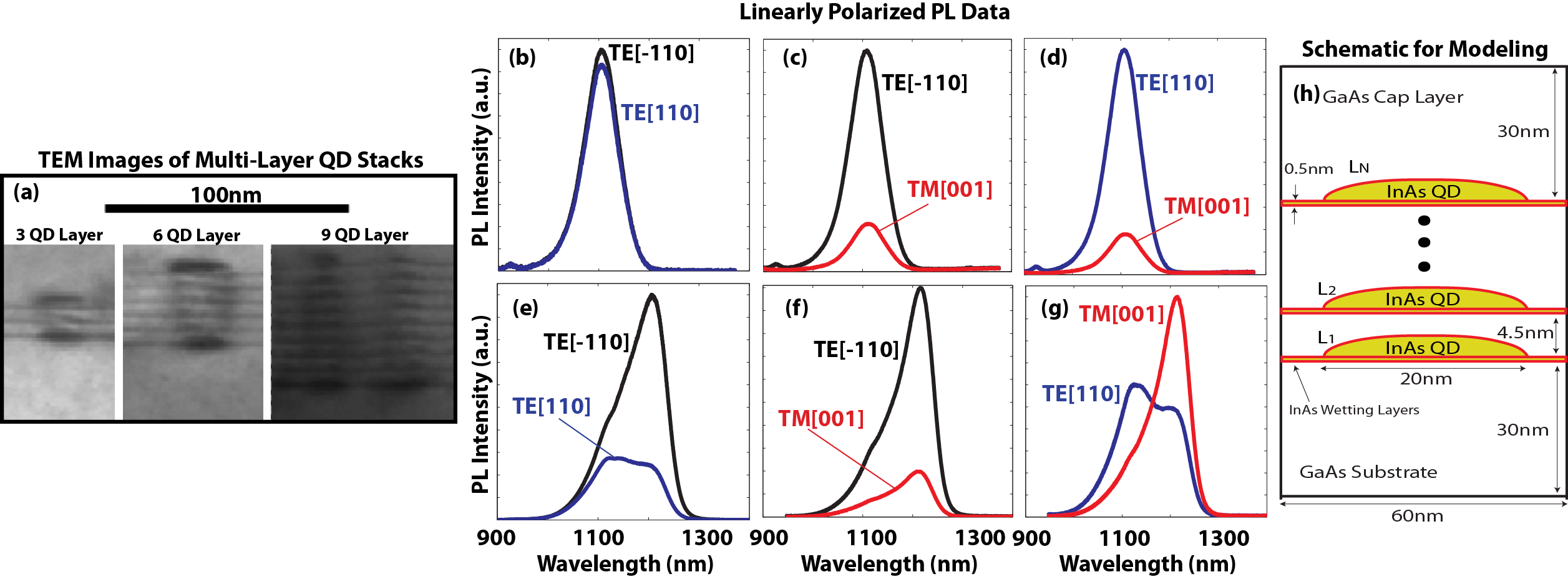
Experimental Procedure: The QD samples are grown on an undoped [001] GaAs subtrate using solid-source molecular-beam epitaxy. First a thick layer of GaAs buffer layer is grown at C, followed by repetitions of the InAs QD layers and GaAs spacer layers with growth interruptions of 10s after each GaAs spacer layer reached a thickness of 16MLs. The nominal thickness of the InAs is kept 1.9ML. Finally the QD layers are capped with a 100nm thick GaAs layer. Further details of our growth process can be found in earlier publicationsInoue_1 ; Inoue_2 ; Inoue_3 ; Inoue_4 . The crystallographic properties of the stacked QDs are examined using a cross-sectional transmission electron microscope (TEM). The TEM images of the samples containing three, six, and nine QD layers are shown in Fig. 1(a)Inoue_1 .
Next, we perform linearly polarized PL measurements at room temperature to investigate the polarization dependent optical spectra. The laser diode excitation is at 659nm wavelength. The detailed set up and measurement procedure is described by T. Inoue et alInoue_2 . The polarization dependent PL spectra are shown in Fig. 1 for a single QD layer (b, c, d) and nine QD layers (e, f, g).
Fig. 1(b, c, d) indicate for a single quantum dot that TE110 and TE show a similar magnitude, and that TM001 has a much smaller response than both in-plane TE-modes. This is typical for InAs QDs and is due to the compressive biaxial strain that splits the HH-LH band edges resulting in HH-type valence band states close to band gap. Previous theoretical and experimental studies on single QDs have shown similar properties.
The PL spectra in the Fig. 1(e, f, g) on contrary reveal an interesting and unique property of the InAs/GaAs QD stacks that the TE110 response is significantly less than the TE response. No previous evidence exists for such TE-mode anisotropy in InAs/GaAs QDs, though Podemski et al.Podemski_1 have reported similar results for InP-based columnar quantum dash structures. The measured difference between the two TE-modes is such that even the DOP for the same QD stack could have different signs when measured along the [110] and [] directions. The reason for such TE-mode anisotropy is highly non-intuitive and requires modeling and simulations of these large QD structures. The modeling must include the correct symmetry properties because the long range strain effects the room temperature material properties and atomistic structure resolution. The multi-million atom simulations presented in this article explains the experimental measurements in terms of hole wave function alignments along the [10] direction.
Theoretical Model: The theoretical modeling of QD stacks containing up to nine QD layers posses a twofold challenge: first it requires an atomistic model that can calculate electronic and optical properties including correct symmetry and interfaces. Secondly the large size of QD stacks requires calculations to be done over millions of atoms to properly include the long-range effects of strain. We use NEMO 3-DKlimeck_1 ; Klimeck_2 to analyse the electronic and optical properties of multi-layer QD stacks. NEMO 3-D is based on fully atomistic calculations of strain and electronic structure: the strain is calculated by using atomistic valence force field (VFF) modelKeating_1 , including anharmonic correctionsLazarenkova_1 to the Keating potential and the electronic structure is calculated by solving a Hamiltonian inside twenty band basisBoykin_1 .
NEMO 3-D has been designed and optimized to be scalable from single CPU to large number of processors on most advanced supercomputing clusters. Excellent MPI based scaling to 8192 cores/CPU has been demonstratedAhmed_1 . The atomistic modeling techniques and parallel coding scheme implemented in NEMO 3-D allows it to simulate large QD stacks with realistic geometry extension and symmetry properties. Past NEMO 3-D based studies of nano-structures include (i) single InAs QD with InGaAs SRCLUsman_1 , InAs bilayer QDsUsman_2 ; Usman_4 , and InAs multi-layer QD stacksMarek_1 , (ii) valley splitting in miscut Si quantum wells on SiGe substrateKharche_1 , (iii) Stark effect of single P impurities in SiRahman_1 , and (iv) dilute Bi impurities in GaAs and GaP materialsUsman_5 .
Simulated System: The theoretical analysis of the multi-layer QD stacks containing up to nine layers is carried out through a set of systematic simulations. The geometry parameters of the QD samples are extracted from the TEM images shown in the Fig. 1(a) which indicates that all the QDs in the stacks are of nearly identical size. Some top most layers in the nine quantum dot stack appears to be relatively small and are only partially grownInoue_1 . The schematic diagram of the system modelled in our simulations is shown in Fig. 1(h). Multiple QD layers separated by 4.5nm thick GaAs buffer are embedded inside a large GaAs matrix. This wetting layer-to-layer separation is experimentally optimized to obtain uniform vertical QD stacks from the self-assembly growth processInoue_2 . Each QD layer consists of a dome-shaped InAs QD with circular base, lying on top of a 1.0ML InAs wetting layer. The QD systems with single, three, six, and nine QD layers will be labelled as L1, L3, L6, and L9, respectively.
The size of QDs extracted from the TEM images indicates a base diameter of 20nm and height of 4nm. Since the height of the quantum dots in the TEM images is not very clear, we choose to simulate three different QD geometries in our theoretical study: (i) All QD layers are identical with 20nm base diameter and 4nm height of the QD in each layer. All the results presented are for this system unless other dimensions are specified. (ii) All QD layers are identical with 20nm base diameter and 3.5nm height of the QD in each layer and (iii) the size of QDs increases from the lower to the upper layers: the base diameter increases by 1nm and the height increases by 0.25nm. We choose this last system (iii) because past experiments of multi-layer QD stacksXie_1 ; Usman_2 have indicated an increasing size of QDs when multi-layer QD stacks are grown by the self-assembly process, so it is interesting to theoretical investigate this geometry. We also simulate a system L9 in which the height of QDs in each layer is 4.5nm. This would mean that the top of each quantum dot will be touching its upper adjacent wetting layer, approaching columnar QD limit. The theoretical results presented here for various QD geometries provide a guide for the experimentalists to understand the dependence of DOP on the QD geometry since experimental investigations of QD stacks for polarization response are still under way.
The QD layers are embedded inside a sufficiently large GaAs buffer to ensure proper relaxation of atoms and to accommodate the long-range effects of strain. The size of the largest GaAs buffer for the system containing nine QD layers L9 is 60x60x106, consisting of 24.4 million atoms. Mixed boundary conditions are applied in the strain minimization: the substrate is fixed at the bottom, the GaAs matrix is periodic in lateral dimensions, and the capping layer is free to relax from the top. The electronic structure calculations use a separate subdomain with closed boundary conditions to reduce the computational burden Klimeck_2 , with a surface passivation Lee_1 which avoids artificial surface states in the atomistic representation.
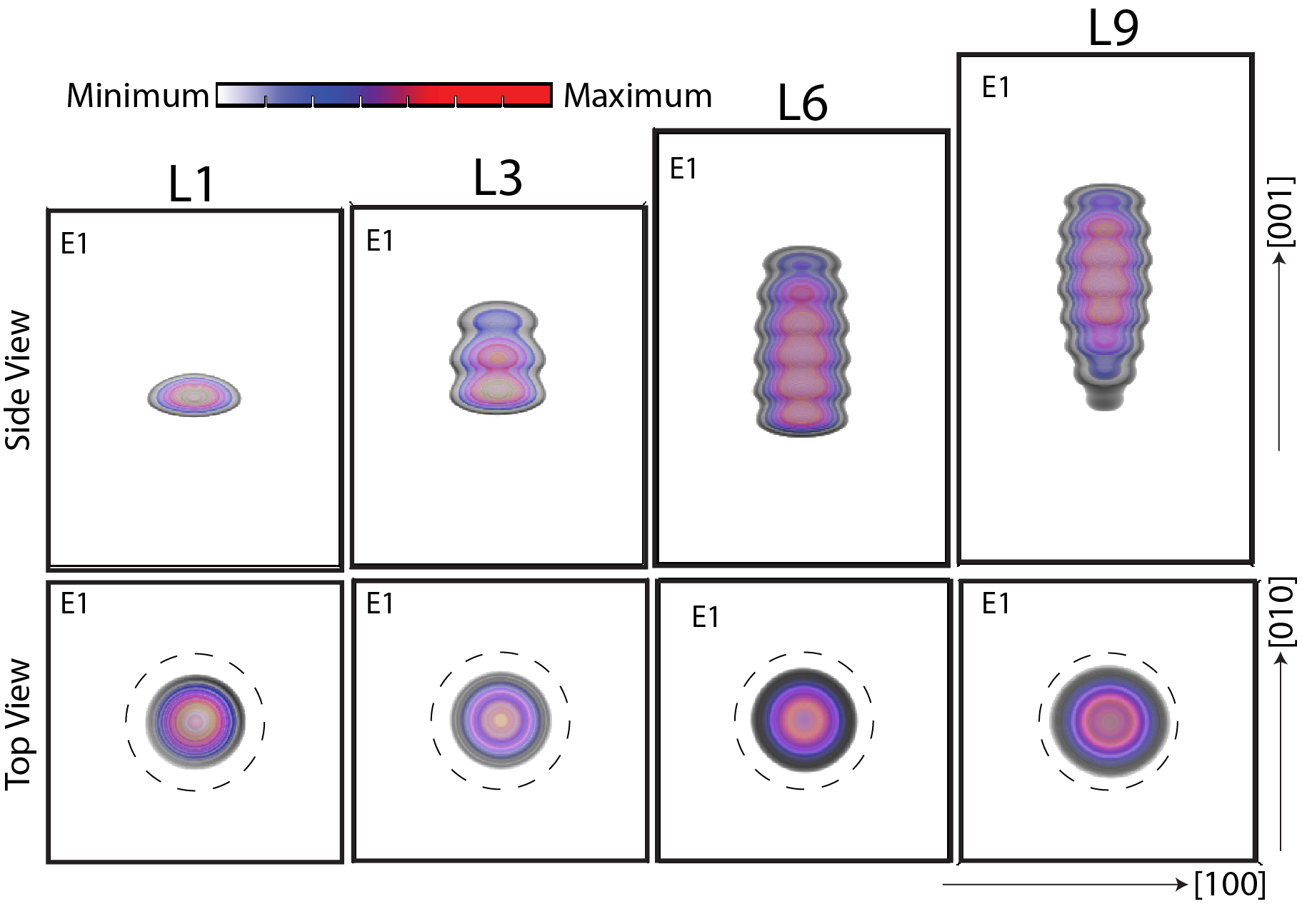
Electron Wave functions form molecular states: Figure 2 shows the plots of the lowest conduction band state E1 for all of the four QD systems under study. From the top views of the wave functions (second row), it is evident that the lowest electron state is of s-type symmetry. The side views of the wave functions (first row) show that the electron state forms a hybridized (molecular) state in L3, L6, and L9 stacks, and is spread over all of the quantum dots. This is due to strong coupling of quantum dots at 4.5nm separation. The presence of the s-like electron wave function in all of the quantum dots implies that only the details of hole wave functions inside the quantum dot stack will determine the optical activity of a particular quantum dot inside the stack. This is different from the previous study of bilayers Usman_2 , where a weak coupling of quantum dots at 10nm separation resulted in atomic like electron wave functions. In the bilayer system, both the electron and the hole wave functions determined the optical activity of the quantum dots. Previous studies on the identical bilayerUsman_4 and stacks with seven identical QDsMarek_1 showed that the strain tends to push the electron states towards the lower QDs in such systems. The electron wave functions for L3 and L6 systems follow this trend. Here we find that this trend is no longer true for stacks with nine QD layers, L9, where the electron wave function E1 vanishes around the edges of the stack due to the larger strain magnitude there (see Fig. 2 first row for L9).
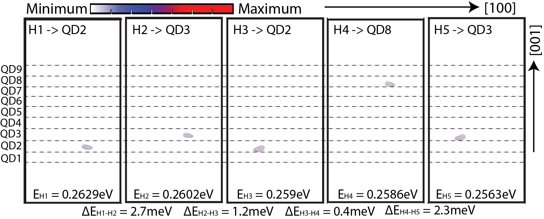
Hole wave functions exhibit atomic character: Although the electrons (lighter-mass particles) are strongly influenced by the inter-dot electronic and strain couplings of QDs and exhibit tunnelling across the quantum dots forming molecular like hybridized states, the holes due to their heavier mass remain well confined inside the individual dots and do not show any hybridization Bester_1 . For example, Fig. 3 show the side views of the lowest five valence band wave functions in the L9 system. The horizontal dotted lines are plotted to mark the positions of the base of the QDs and helps to determine the location of a particular hole wave function inside the stack. In this system, H1 and H3 are inside QD2, H2 and H5 are in QD3, and H4 is in QD8. The location of a hole state inside a QD stack is relatively hard to determine and is strongly influenced by geometry of the QD stack i.e. QD base diameter, QD height, QD layer separation etc. Ultimately the strain profile that controls the strength of the coupling between the QD layers inside the stack determines the position of the hole states inside the stacks.
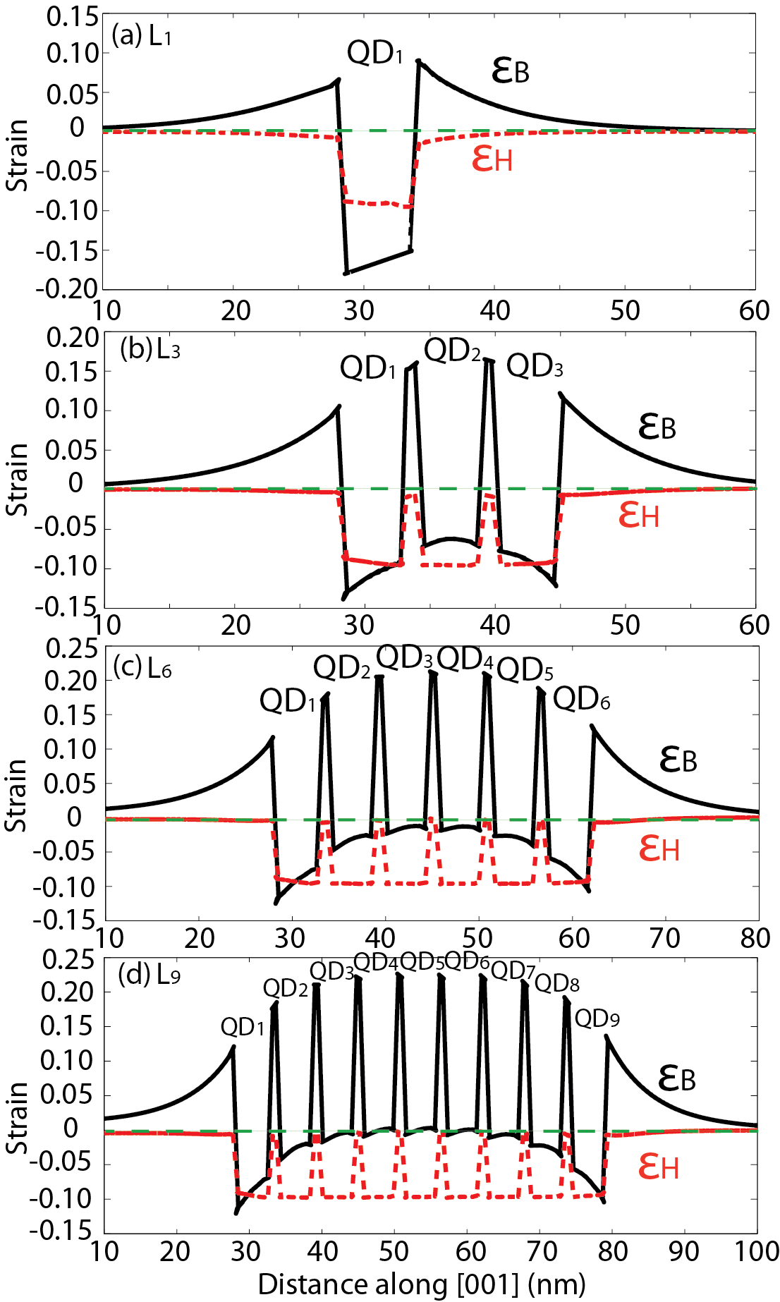
Hydrostatic and Biaxial Strains: Figure 4 plots the hydrostatic (dotted lines) and biaxial strain (solid lines) profiles along the [001] direction through the center of the quantum dots. The hydrostatic strain exhibit a very slight change from L1 to L9. The biaxial strain however significantly changes as the QD stack height increases. For a single QD, L1, the biaxial strain is highly negative inside the QD region. As the vertical size of the QD stack is increased by adding QD layers, the biaxial strain at the center of the stack reduces. For the L9 stack in the Fig. 4(d), the biaxial strain at the center of the stack approaches zero. The reason for such behaviour of the biaxial strain is that in general the InAs unit cells inside the QD region tend to fit over the GaAs matrix by an in-plane compression and an elongation along the [001] direction. This results in highly negative biaxial strain as can be observed for a single QD in the Fig. 4(a). However, when the size of the stack increases, the unit cells of InAs around the center of the stack feel lesser and lesser compressive force from the surrounding GaAs. As a result, the vertical lattice constant of the InAs starts matching with the GaAs and hence the biaxial strain tends to change its sign around the middle of the QD stack. Similar strain profiles were calculated in an earlier study about columnar QDs by T. Saito et al.Saito_1 .
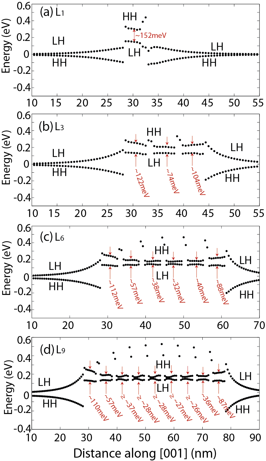
Increased HH-LH Mixing: The minor change in the magnitude of the hydrostatic strain (as L1 L9) implies that the lowest conduction band edge will experience very small change as they are only effected by the hydrostatic componentUsman_1 . The valence band edges are affected by both the hydrostatic strain as well as the biaxial strain. The impact of strain on the highest two valence band edges, HH and LH, is analytically expressed as:
| (2) |
| (3) |
Here and are deformation potential constants for HH and LH band edges. The values for these constants for InAs systems are = 1.0eV and = -1.8eV, respectivelyUsman_1 . From the equations 2 and 3, it is evident that the magnitude of the determines the HH-LH splitting. For a single QD layer, due to large negative value of , the HH and LH band edges will be considerably separated inside the QD region. This will induce dominant HH character in the highest few valence band states which will be closer to the HH band edge. As the magnitude of decreases, the HH-LH splitting reduces, increasing LH component in the valence band states. For the L9 system, the nearly zero magnitude of the around the center of the stack implies that the HH and LH bands will be nearly degenerate around the center of the QD stack. The valence band states will therefore be of highly mixed character, consisting of contributions from both the HH and the LH bands.
Figure 5(a-d) plots the highest two local valence band edges, HH and LH, for all of the QD systems under study along the [001] direction through the center of the QDs. Highly negative biaxial strain in L1 results in 152meV splitting of HH and LH bands within the QD region. As the biaxial strain around the center of QD stack decreases (approaching towards zero), the HH-LH splitting around the center of the stack also decreases to 74meV, 32meV, and 28meV for the L3, L6, and L9 systems, respectively.
The HH and LH character of a particular valence band state in the tight binding formulation can be estimated as follows: If the amplitudes of the px, py, and pz orbitals at any atomic site are ax,u/d, ay,u/d, and az,u/d respectively (where the subscripts and refer to up and down spin), then the HH contribution is approximately proportional to + summed over all the atomic sites. The LH contribution is approximately proportional to + summed over all the atomic sites. By using these expressions, we estimate that the ratio for the highest valence band state (H1) decreases from 108 for the L1 to 15.8, 12.3, and 10.6 for the L3, L6, and L9 systems, respectively. This clearly points towards an increasing LH character in the valence band states as the height of the QD stack increases.
HH/LH intermixing implies TM001-mode increases: In a QD system, the HH states consist of contributions from px and py orbitals and the LH states consist of contributions from px, py, and pz orbitalsSingh_1 . These configurations imply that the TM-mode (which is along the z-direction) will only couple to the LH states. The large splitting of the HH-LH bands (see Fig. 5(a)) resulting in a weak LH contribution in the L1 system will result in very weak TM001-mode for this system. Thus from Eq. (1), the DOP will be nearly 1.0 and the polarization response will be highly anisotropic. As the size of the QD stack increases, the larger intermixing of HH and LH bands increases LH contribution in the valence band states. This will result in increase of TM001-mode of optical transitions reducing the anisotropy of DOP bringing it closer to 0.
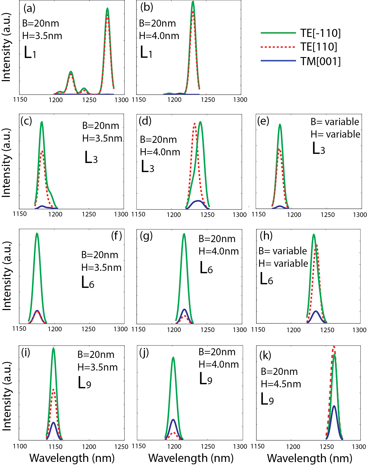
Optical intensity functions, f(): Figure 6 plots the optical intensity functions computed from our model as a function of the optical wavelength for various quantum dot systems. The calculation of the optical intensity function is done as follows: first we calculate optical transition strengths by using Fermi’s golden ruleUsman_2 for TE110-, TE-, and TM001-modes between the lowest conduction band state E1 and the highest five valence band states H1, H2, H3, H4, and H5 for a particular QD system. Next each optical transition strength is artificially broadened by multiplication with a Gaussian distribution centred at the wavelength of the transitionStier_1 ; Singh_2 . Finally we add all of the five Gaussian functions to calculate the total optical intensity function, f(). The complete expression for the optical intensity function, plotted in the Fig. 6(a-k), is given by equations 4 and 5:
| (4) |
where,
| (5) |
The examination of the optical intensity plots in the Fig. 6 reveals that the TM001-mode indeed increases as the size of QD stack is increased: L1 L9. This is in general true for all of the geometry configurations considered and is a direct consequence of the change in the biaxial strain component that increases HH and LH intermixing as discussed earlier.
Increase in TM001 only partially contributes towards isotropic polarization: Fig. 6 shows that the increase in the TM001-mode only partially helps towards an isotropic polarization response. This is in contrast to a general notion where it is described that the increase in the TM001-mode is mainly responsible for the isotropic polarization.The reason for such understanding is that the previous theoreticalSaito_1 or the experimental studiesInoue_1 ; Ridha_1 ; Fortunato_1 of the DOP have assumed only one direction for the TE-mode. However, our PL measurements in the Fig. 1(e-g) show that the TE-modes along the [110] and [] have significant anisotropy in the plane of the QD stack. The theoretical model shows that in fact a major contribution to achieve isotropic polarization response in these systems stems from a suppressed TE110-mode rather than an increased TM001-mode. Fig. 6 shows that irrespective of QD geometry, the increase in the TM001-mode is insufficient to reverse the sign of the DOP (+ -).
The TE-mode is highly anisotropic in the plane of the QD with the magnitudes of the TE110- and TE-modes becoming very different as the QD stack size increases. For a single QD system, L1, TE TE and TM001 is very weak. Hence the measured and calculated DOP is highly anisotropic (close to 1.0) irrespective of the direction for the TE-mode. As the QD stack size increases, the TM001-mode also increases partially contributing to reduction in the DOP. However, at the same time, the TE110-mode decreases considerably such that for L6 and L9, it becomes smaller than the TM001-mode. The reason for such a drastic decrease in the TE110-mode is the orientation of hole wave functions along the [10] direction for the L6 and L9 systems.
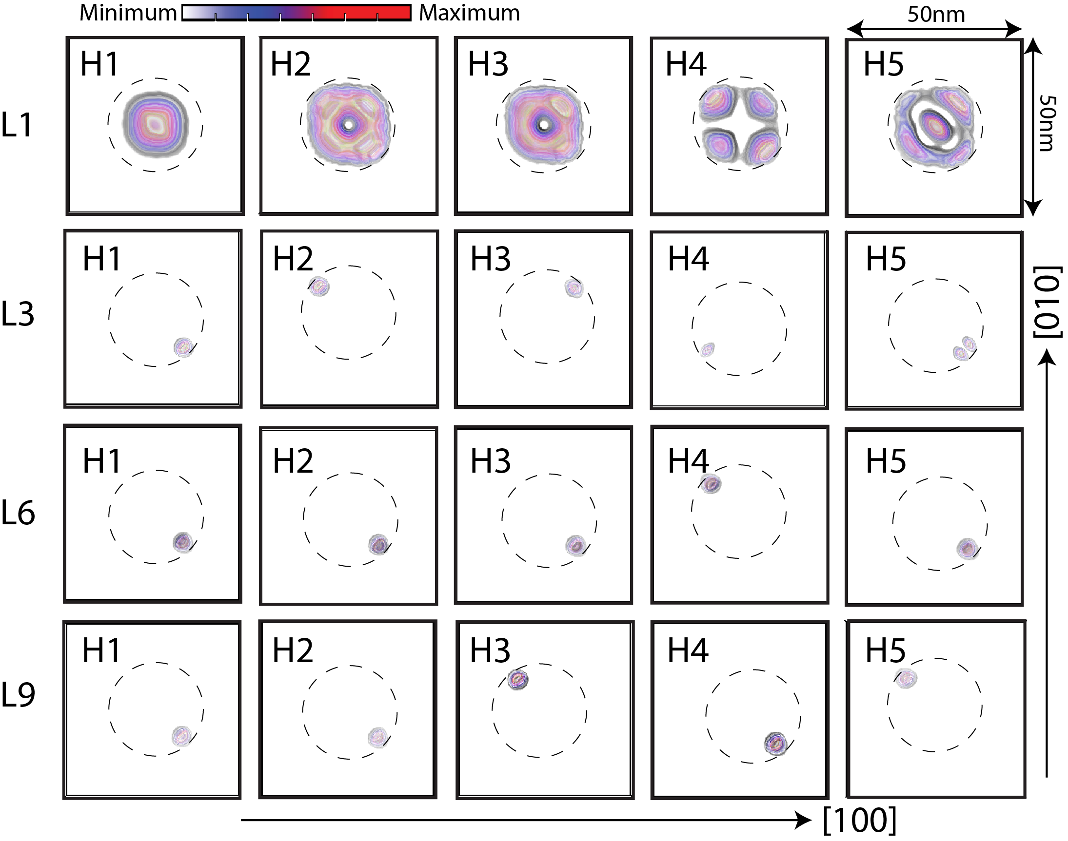
Hole wave functions are oriented along [110] and resulting in : Figure 7 plots the top views of the highest five valence band states H1, H2, H3, H4, and H5 for the QD systems L1, L3, L6, and L9. The five hole wave functions for the L1 system have an almost uniform distribution inside the QD region with nearly symmetric shape. Such symmetry will result in approximately equal magnitude of TE-mode along the [110] and directions, as evident in the first row of the Fig. 7. For the stacks with three, six, and nine QD layers, the distribution of the hole wave functions is oriented along the [110] or [10] directions. This [110]/-symmetry is mainly due to the strain and piezoelectric potentials that lowers the overall symmetry of the QD system and favours these two directionsBester_1 ; Usman_1 . To verify the impact of the strain and piezoelectricity, if we conduct a numerical experiment and switch off their contributions in the electronic structure calculations, the TE/TE110 ratio for the L6 system decreases from 10.92 to 0.85 and it decreases from 10.73 to 3.2 for the L9 system. Similar distributions of the hole wave functions are observed for bilayersUsman_2 and a single QD layer with aspect ratioUsman_3 (H/B) 0.25.
The orientation of the hole wave functions determines the magnitude of the TE110- and TE-modes since the lowest electron wave function (see Fig. 2) is symmetrically distributed. For L3, the hole wave functions H1, H2, and H5 are oriented along the [10] direction, while the other two hole wave functions H3 and H4 are oriented along the [110] direction. The orthogonal distributions of the hole wave functions in L3 will result in similar [110] and [10] TE-modes. The cumulative summations for the TE110 and TE-modes arising from these five hole states are indeed nearly equal, with TE magnitude being slightly larger as can be seen in the Fig. 6(d).
All of the highest five hole wave functions are oriented along the [] direction in case of the L6 and L9 systems. This results in a strong reduction of the TE110-mode. The significant reduction in the TE110-mode turns out to be even smaller than the magnitude of TM001-mode as can be seen in the Fig. 6(f, g, j). This change in relative magnitude results in a flip of sign (+ -) for DOP110 as indeed measured in the experimentInoue_1 . Hence we conclude that the isotropic polarization response demonstrated by the experiment is a result of two factors: (i) increase in the TM001-mode due to enhanced HH-LH intermixing and (ii) the reduction of TE110-mode due to orientation of holes along the [] direction.
Here we want to point out that the relative magnitude of the TE-mode does not reduce as the size of the QD stack is increased. Even for the largest system under study, L9, the TE-mode is much stronger than the TM001-mode. That means if the experimental measurements are performed for DOP, they should still show anisotropy. This is verified by our PL measurements on L9 system shown in Fig. 1(f). These PL measurements on L9 system indicate a positive value for the DOP (TE TM001) and a negative value for the DOP110 (TE110 TM001).
Comparison with experimental PL data: Table 1 summarizes the calculated values of DOP from our model along different directions and compares it with the experimental PL measurements. Here we provide theoretically calculated values of DOP along [100] and [010] directions for comparison purpose because some recent experimental studies have chosen these directions for investigation of the DOP and characterization of the polarization response of the QD systemsFortunato_1 ; Saito_1 ; Ridha_2 .
| QD Geometry | Theoretical Calculations | Experiment | |||||
| LN | (B, H) (nm) | DOP100 | DOP010 | DOP110 | DOP | DOP110 | DOP |
| L1 | (20, 3.5) | 0.995 | 0.996 | 0.996 | 0.996 | 0.7 | 0.71 |
| (20, 4.0) | 0.999 | 0.999 | 0.999 | 0.999 | |||
| L3 | (20, 3.5) | 0.922 | 0.884 | 0.9046 | 0.933 | 0.67Inoue_1 | |
| (20, 4.0) | 0.77 | 0.77 | 0.833 | 0.836 | |||
| (V, V) | 0.929 | 0.929 | 0.916 | 0.94 | |||
| L6 | (20, 3.5) | 0.594 | 0.594 | 0 | 0.747 | 0.46Inoue_1 | |
| (20, 4.0) | 0.548 | 0.46 | -0.244 | 0.72 | |||
| (V, V) | 0.733 | 0.733 | 0.73 | 0.76 | |||
| L9 | (20, 3.5) | 0.6 | 0.6 | 0.445 | 0.652 | -0.6Inoue_1 , -0.36 | 0.66 |
| (20, 4.0) | 0.38 | 0.371 | -0.45 | 0.603 | |||
| (20, 4.5) | 0.45 | 0.446 | -0.47 | 0.43 | |||
The hole state symmetries shown in the Fig. 7 show strong alignment in the [110] and [] directions indicating that symmetries to the [100] and [010] directions will be almost equivalent. Therefore the values of the DOP are nearly equal for the [100] and [010] directions as mentioned in the table 1. The PL measurements along these two directions will not exhibit isotropic polarization even for the L9 system. Similar results were found in an earlier experimental study by P. Ridha et al.Ridha_2 . In their study of the polarization properties of multi-layer stacks based on TE010-mode, they conclude that such systems can not provide isotropic polarization and columnar QDs are the only choice.
For the system L1 containing only a single QD layer, our calculated DOP values in all the directions are very close to 1.0, exhibiting a very strong polarization anisotropy (TE-mode TM-mode). The experimentally measured values for this system are relatively low (0.7), but they also show that the value of the DOP remains nearly the same irrespective of the measurement direction. While the reason for difference between our calculated value and the measured value for this QD system is not very clear, other theoretical studies using k.p methodSaito_1 ; Sheng_1 on single QD layers with similar dimensions have also presented the values of the DOP close to 1.0.
Sensitivity of the DOP with the QD stack geometry parameters: Since the heights of the QDs in the experimental TEM images are not very clear (see 1(a)), so we simulate various geometry configurations of the QD stacks and provide the values of the DOP in the table 1. This data serve as a measure of the sensitivity of the DOP with respect to the QD stack geometry parameters and provide a guide to experimentalists to explore the design space of such complex multi-million atom systems. From the table 1, as the QD stack height increases in the L1 L3 L6 L9, the value of the degree of polarization reduces. The reduction in the value of the DOP is larger for the stacks with H=4.0nm as compared to the stacks with H=3.5nm. This is due to the fact that the larger height of QDs in the stack results in stronger coupling between the QDs. This implies a stronger HH-LH intermixing resulting in larger magnitude of the TM001-mode.
The dependence of the DOP on the height (H) of the QDs inside the stacks is an unknown factor. The calculated values of the DOP in the table 1 shows that the DOP becomes very sensitive to the height of the QDs inside the stack as the size of the stack grows larger. For the systems L1 and L3, the increase in the height (H) from 3.5nm to 4.0nm results in a small decrease in the values of the DOP. However, for a same change in the value of H, the DOP110 significantly decreases from 0 to -0.244 and from 0.445 to -0.45 for the L6 and L9 systems, respectively. This implies that an isotropic polarization response (DOP 0) can either be achieved from the L6 stack with H=3.5nm, or from a stack with fewer number of QD layers and H=4.0nm. We therefore propose that the polarization response of the QD stacks can be tuned by not only increasing the number of QD layers (a parameter tuned in the past experimental studiesInoue_1 ; Ridha_1 ; Ridha_2 ; Saito_1 ; Kita_1 ), but also by controlling the height (H) of the individual QDs inside the stacks.
The calculations on the L3 and L6 systems, where the size of QDs is increased as the stack size increases, indicate that such stacks with non-identical QD layers will exhibit relatively higher values of the DOP and hence will not be suitable for isotropic polarization response. The same is true for the case when the height of the QDs in the L9 system is increased to 4.5nm such that the adjacent QD layers touch each other (approaches columnar QD limit). Based on the comparison of the calculated and the measured values of the DOP for the L9 system in the table 1, we estimate that the dimensions of the QDs inside the stacks are approximately B=20nm and H=4nm.
Conclusions: This article presents a detailed analysis of the polarization response of the multi-layer QD stacks by PL measurements and through a set of systematic multi-million atom tight binding electronic structure calculations. Our theoretical results follow the trends of the experimental measurements on quantum dot stacks containing single, three, six and nine QD layers and provide significant physical insight of the complex physics involved by analysing the strain profiles, the band edge diagrams, and the wave function plots. The experimentally measured PL data for the nine quantum dot stack reveals a unique property by indicating a significant difference in the DOP for the [110] and [] directions. We explain here that this difference is due to the orientation of the hole wave functions along the [] direction that results in significant reduction of the TE-mode along the [110] direction. We suggest that the isotropic polarization response from the multi-layer QD stacks is due to two factors: (i) the reduction of the TE110-mode direction and (ii) the increase in the TM001-mode due to enhanced LH-HH intermixing. Our result presented in this paper for various geometry configurations serve as guidance for the experimentalists to design future QD based optical devices. A flip of sign for the DOP in our PL measurements and theoretical calculations as the size of QD stack increases indicates significant potential to achieve polarization insensitive response from multi-layer QD stack systems.
Acknowledgements: Muhammad Usman gratefully thanks Dr. Susannah Heck (OCLARO, UK) for useful discussions about the polarization response of the QD samples. Computational resources accessed through the nanoHUB.org application ”Workspace” operated by the NSF funded Network for Computational Nanotechnology are acknowledged. The back-end supercomputers are operated by the Rosen Center for Advanced Computing (RCAC), Purdue University.
References
- (1) M. Usman et al., IEEE Trans. Nanotechnology, 8, 330-344 (2009)
- (2) J. Tatebayashi et al., Applied Physics Lett. 78, 3469 (2001)
- (3) P. Ridha et al., IEEE Journal of Quantum Electronics, 46, 197-204 (2010)
- (4) T. Saito et al., Phys. Rev B 77, 195318 (2008)
- (5) T. Kita et al., Jpn. J. Appl. Phys., Part 2 41, L1143 (2002)
- (6) T. Kita et al., Appl. Phys. Lett. 88, 211106 (2006)
- (7) O. Kojima et al., J. Appl. Phys. 103, 113504 (2008)
- (8) O. Kojima et al., J. Appl. Phys. 107, 073506 (2010)
- (9) M. Usman, et al., J. of Appl. Phys., 109, 104510 (2011)
- (10) L. Fortunato et al., Superlattices and Micsostructures 47, 72-77 (2010)
- (11) P. Podemski et al., Applied Phys. Letters 93, 171910 (2008)
- (12) T. Inoue et al., Appl. Phys. Lett. 96, 211906 (2010)
- (13) G. Klimeck et al., IEEE Trans. on Electron Devices 54, 2079-2089 (2007)
- (14) G. Klimeck et al., IEEE Trans. on Electron Devices 54, 2090-2099 (2007)
- (15) P. Keating et al., Phys. Rev. 145, 637 (1966)
- (16) L.O. Lazarenkova et al., Appl. Phys. Lett. 85, 4193-4195 (2004)
- (17) T.B. Boykin et al., Phys. Rev. B 66, 125207 (2002)
- (18) Q. Xie et al., Phys. Rev. Lett. 75, 2542-2545 (1995)
- (19) T. Inoue et al., Proceedings of SPIE, vol. 7597, 75971J-1 (2010)
- (20) M. Korkusinski et al., J. of Physics: Conference Series, 38, pg. 75-78 (2006)
- (21) S. Lee et al., Phys. Rev B 66, 235307 (2002)
- (22) M. Usman et al., under review with J. of Appl. Phys., arXiv:1012.3489 (2010)
- (23) Y. Ikeuchi et al., accepted for publication in Appl. Phys. Express, 2011
- (24) J. Singh, Semiconductor Optoelectronics, McGraw-Hill, New York, 1995
- (25) M. Richter et al., Appl. Phy. Lett., 88, 231902 (2006)
- (26) H. Liu et al., Appl. Phy. Lett., 86, 143108 (2005)
- (27) J. Jiang et al., Appl. Phy. Lett., 84, 2166 (2004)
- (28) M. Usman et al., proc. of IEEE Nano, Arlington TX, pg. 541-544, (2008)
- (29) S. Ahmed et al., Springer Encyclopaedia of Complexity, 2008, arXiv:0901-1890v1
- (30) R. Rahman et al., Phys. Rev Lett., 99, 036403 (2007)
- (31) N. Kharche et al., Appl. Phy. Lett., 90, 092109 (2007)
- (32) M. Usman et al., under preparation, 2011
- (33) P. Ridha et al., Opt. Quant. Electron, 40, pg. 239-248 (2008)
- (34) G. Bester et al., Phys. Rev B 72, 165334 (2005)
- (35) G. Bester et al., Phys. Rev B 71, 045318 (2005)
- (36) T. Inoue et al., J. of Physics: Conference Series, 245, (2010) 0120761
- (37) W. Sheng et al., Appl. Phys. Lett. 80, 2755 (2002)
- (38) O. Stier et al., Phys. Rev B, 59, 5688 (1999-II)
- (39) Y.-Y. Lin et al., J. of Appl. Phys. 92, 6205 (2002)