Transmission enhancement in three-dimensional rolled-up plasmonic metamaterials containing optically active quantum wells
Abstract
We investigate three-dimensional rolled-up metamaterials containing optically active quantum wells and metal gratings supporting surface plasmon polarition resonances. Finite-difference time-domain simulations show that by matching the surface plasmon polarition resonance with the active wavelength regime of the quantum well a strong transmission enhancement is observed when illuminating the sample with p-polarized radiation. This transmission enhancement is further increased by taking advantage of the Fabry-Perot resonances of the structure.
pacs:
81.05.Xj, 78.67.Pt,73.20.MfI Introduction
The emerging field of metamaterials and the realization of materials exhibiting a negative index of refraction (NIM) in the past ten years opened the way for various fascinating applications. With these novel materials physical applications like cloaking devices Schurig et al. (2006); Cai et al. (2007); Ergin et al. (2010) and optical imaging beyond the diffraction limit Liu et al. (2007a); Zhang and Liu (2008); Kawata et al. (2009) have become possible. A metamaterial consists of artificial structures which are much smaller than the wavelength of the operating incident radiation. NIMs have been realized by metal-dielectric structures e.g. split-ring resonators deposited on dielectrics Shelby et al. (2001); Katsarakis et al. (2005) or fishnet structures Zhang et al. (2005); Dolling et al. (2006); Xiao et al. (2009). However, due to the electron-beam lithography fabrication process of these structures, the realization of three-dimensional metamaterials requires a sequentially stacking of single layers Dolling et al. (2007); Liu et al. (2007b); Valentine et al. (2008). Three-dimensional metamaterials consisting of multistacks of metal-dielectric layers can also be obtained by rolling-up strained layers into microrolls Prinz et al. (2000); Schumacher et al. (2005). That opens up the application of such microrolls for example as hyperlenses Schwaiger et al. (2009).
The efficiency of metamaterials suffers from the absorption of radiation in the metal, caused by the finite imaginary part of the metals dielectric function. This causes strong energy dissipation and a rapid field decay. A possible solution to overcome this problem would be the incorporation of gain materials. Different approaches in the recent literature include dyes Xiao et al. (2010), quantum dots Plum et al. (2009) and optically-pumped quantum wells that have been brought in close proximity to split-ring resonators Meinzer et al. (2010). Semiconductor quantum wells show no bleaching and electrical pumping is well established for these structures. Recently it was demonstrated that the self-rolling process offers the possibility to easily include active quantum-wells in the semiconductor layer of three-dimensional metamaterials. It was found that such a novel structure shows enhanced light transmission upon optical pumping Schwaiger et al. . In the next step the concept of rolled-up nanotech allows the realization of three-dimensional metamaterials with sophisticated metallic nanostructures instead of planar metal layers which enables us to profit from plasmonic resonances.

In this letter we investigate alternating layers of amplifying quantum wells and metal gratings supporting surface plasmon polaritions (SPPs). Such structures can be realized in the walls of rolled-up metamaterials as sketched in Fig. 1. Experimentally one can prepare different type of layered systems rolling along or perpendicular to the grating stripes. Here we are interested in the fundamental effect of grating coupler enhanced gain and concentrate on a microroll with rolling direction along the grating stripes where we can precisely align the stripes on top of each other. Whereas in the case of a perpendicular rolling direction commensurability effects between the microroll perimeter and the grating period can occur. We present finite-difference time-domain (FDTD) simulations which show a transmission enhancement in the structures with metallic gratings much larger than observed for samples with flat silver surfaces.
II Structures and Simulation Method
In Fig. 1 a sketch of a microroll is shown. The preparation of this structures is based on strain relaxation of pseudomorphically grown (AlIn)GaAs heterostructures, which roll up into a tube when released from the substrate by etching away an AlAs sacrificial layer (for details see Schwaiger et al. (2009)). The important ingredients for our investigation here is that in addition (i) an InGaAs gain layer and (ii) a grating is etched into the semiconductor layer and covered with Ag before the rolling-up process. As a result one obtains alternating layers of quantum wells and Ag gratings.

We performed finite-difference time-domain simulations on the metamaterials by using the commercial software Lumerical FDTD Solutions Lumerical Solutions . For the simulations we neglected the curvature of the actual structure and investigate flat structures in two dimensions. We simulated a grating unit cell (lattice constant and filling factor where denotes the width of the etched region) with three layers where we used periodic boundary conditions in x direction and perfectly matched layer boundary conditions in y direction (Fig. 2). We irradiated the investigated structures with a plane wave with zero incident angle. To fulfill the criterion for SPP excitation we assume that this plane wave has the H field and the E field . Due to the periodic corrugation also y components of the electric field are induced. In the frequency spectrum the plane wave pulse has a Gaussian-shaped distribution with a maximum at THz and a full-width-half-maximum (FWHM) of THz. This corresponds to broadband excitation with a center wavelength of nm and a FWHM of nm. Inside the simulation volume we used an appropriate non-uniform mesh which has been optimized by convergence testing. The transmission spectrum was recorded in a distance of m in y direction behind the structure. For the dielectric functions we take polynomial fits on experimental data from Palik Palik (1985). The dielectric functions of the AlGaAs, the InGaAs and the AlInGaAs used in the simulations are based on the dielectric function of GaAs and were adjusted as follows: The percentage of In and Al in the semiconductor layer decreases and increases the bandgap of the composite semiconductor which we assume to be Al26Ga74As, In16Ga84As and Al20In16Ga64As. In first approximation this shift of the bandgap is linear causing the dielectric function to change slightly. This effect was taken into account by dislocating the dielectric function of GaAs linearly,
where and are the percentages of In and Al in the semiconductor, respectively. The difference of the bandgap of GaAs and In53Ga47As Goetz et al. (1983) is eV and the difference of the bandgap of Al30Ga70As and GaAs Monemar et al. (1976) is eV.
The amplification effect of the InGaAs quantum well can be described by a negative imaginary part of the refractive index. In the simulations the dielectric function of this gain layer was modelled qualitatively as a Lorentz oscillator according to Govyadinov et al. (2007):
with as the Lorentz oscillator strength, the damping frequency and as the resonant frequency of the quantum well.
III Parameter calibration
The beneficial exploitation of the SPP excitations on the transmission requires that the lattice constant of the metallic grating is chosen appropriately to adjust the energy of the SPP resonance to the active wavelength regime of the of the quantum well. Furthermore it is favorable to tune the SPP resonance energy to the Fabry-Perot transmission peak of the system arising from the layered semiconductor/metal system with its high index of refraction.

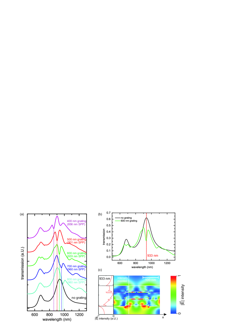
The optically active wavelength regime of the quantum well can in fact be tailored by the amount of Indium used during sample preparation. In the simulations presented in this letter we consider a quantum well emitting at nm. The Fabry-Perot resonance peaks can be shifted by varying the individual layer thicknesses. The black line in Fig. 3(a) shows the simulated transmission spectrum for a three-layer structure with each layer consisting of nm Ag, nm AlInGaAs, nm InGaAs and nm AlGaAs. We see that, for this dimensions, the structure exhibits a pronounced Fabry-Perot peak at the desired wavelength of nm. The appropriate grating was examined by performing simulations with various lattice constants. In Fig. 3(a) we display the transmission spectra for different gratings in comparison with the spectrum of unstructured layers. We first choose a grating filling factor , a depth nm and an Ag thickness nm. One can see that for an nm grating a deep SPP resonance is located at the desired wavelength of nm. For smaller grating periods the SPP resonance shifts to shorter wavelengths (nm for an nm grating and nm for an nm grating) whereas for larger grating periods the SPP-resonance wavelength is longer (nm for an nm grating and nm for an nm grating). Variations in the lattice depth do not affect the position of the SPP resonance but a smaller lattice depth causes less pronounced resonances. Moreover, several other SPP excitations can be observed, however, they are considerably less pronounced. From the observed resonance positions we can reconstruct a dispersion relation where is the diffraction order. We find that the pronounced minima, starting for nm at nm, follow a dispersion with . The minima in the regime between to nm follow the same dispersion with , thus they represent a higher diffraction order. This dispersion lies inbetween the SPP dispersion of a flat-Ag/vacuum interface and a flat-Ag/GaAs interface. This is what we actually expect for our complex semiconductor/metal structures including vacuum gaps. We further expect even different SPP branches due to the asymmetric arrangement and coupling between the three metal layers. Indeed, the resonances starting for nm at nm follow a dispersion that lies energetically below . Our studies showed that the variation of the lattice filling factor (we simulated filling factors between and ) does effect the position of the SPP resonance only slightly by about nm. In Fig. 3(b) we independently show the transmission spectra for the above structure without and with an nm grating. It can be seen clearly that the SPP resonance and the Fabry-Perot resonance peak are matched to the active wavelength regime of the quantum well (nm). In Fig. 3(c) we plot the two-dimensional electric-field distribution of the nm SPP mode (adjacent we show the one-dimensional intensity profile corresponding to the white dashed line). We recognize that the intensity profile exhibits a large intensity inside the structure in particular at the quantum well locations. We note that in two-dimensional metamaterials the gain material has to be brought in very close proximity to the metallic structure (see, e.g., reference Meinzer et al. (2010)) which can cause manufacturing problems. In our three-dimensional case the mode pattern allows us to use thick barrier layers which are necessary to maintain the optical quality of the quantum well and still have a strong field-coupling to the quantum well.


IV Results and Discussion
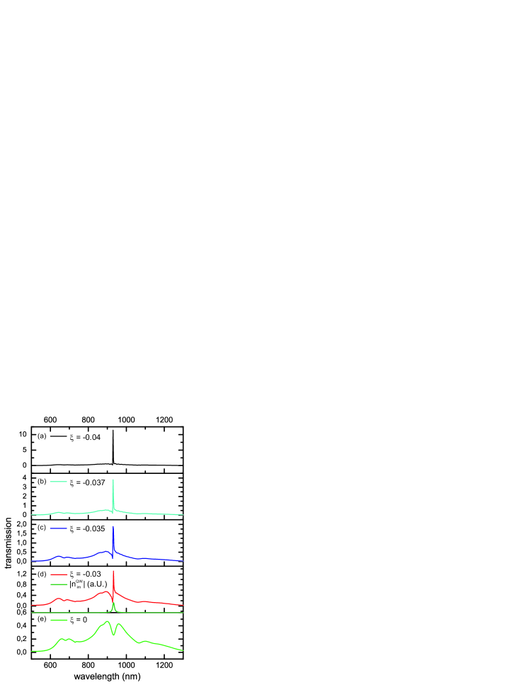
The Lorentz oscillator strength in the gain layer was adjusted by investigating the transmission enhancement on a single layer: In previous experiments without grating it was shown, that for single layers with and without a gain layer, which exhibit transmissions and , respectively, a transmission enhancement of about is easily realizable Schwaiger et al. . We performed simulations where we adjusted the Lorentz-oscillator strength to . This corresponds to single layer transmission enhancements of and imaginary parts of the Lorentz-oscillators refractive index of and at nm, respectively. The results are plotted in Fig. 4. Figure 4(e) shows the transmission spectrum with no gain as a reference. Figures 4(a)-(d) depicts the transmission versus wavelength spectra for the above mentioned values of . It is observed that the transmission at the SPP resonance is drastically enhanced with increasing gain. For (corresponding to and for an unstructured single layer film) we already obtain a transmission of more than at the wavelength of nm. With increasing gain the transmission at this wavelength increases up to 10 for (, ). Figure 3(c) shows that there is a high intensity in all three layers. This indicates that the multilayered systems that we can realize with the microroll technique is indeed quite helpful. We have actually performed simulations, where we selectively turn on the gain in different layers and it turned out that the effects on the transmission are considerably smaller. It is therefore advantageous to use a structure with three or even more layers. We like to note that, as observed in Fig. 4, the transmission enhancement has actually a Fano-type shape with a minimum at the low wavelength side. This indicates that the negative imaginary part of the gain material shifts the SPP resonance position, i.e. there is an increasing interaction between the SPP and the gain layer.
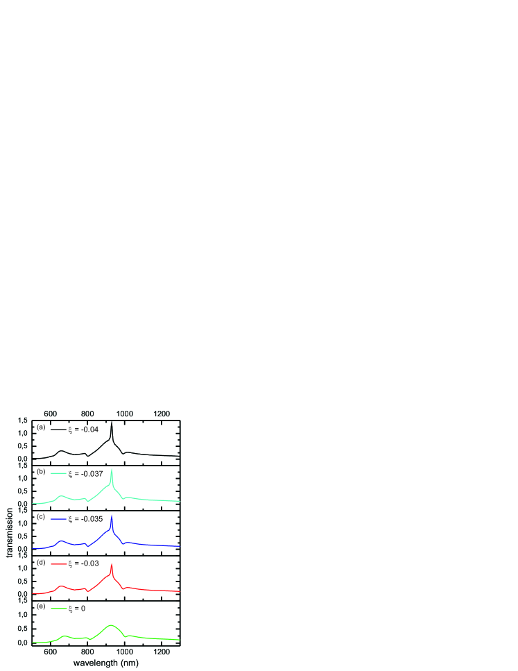
While the excitation of SPPs is linked to illumination with p-polarized light we also performed for comparison simulations in s polarization. The transmission versus wavelength spectra of this run are presented in Fig. 5. Figures 5(a)-(d) show the spectra for Lorentz-oscillator strengths corresponding to and , respectively. Figure 5(e) depicts the transmission spectrum without gain. As expected, there are no SPP resonances. Turning on the gain leads to an increasing transmission at the resonant frequency of the quantum well. However, in the s-polarized case a strong transmission enhancement as in Fig. 4(a)-(d) is not observed. Our simulations show that the increased transmission for s polarization is comparable to simulations with flat layers instead of a grating. This observation supports that the SPP resonances are crucial for the extraordinary transmission. Further simulations show that the strength of the transmission enhancement as seen in Fig. 4 is strongly dependent on the interplay of the Fabry-Perot resonance, the SPP resonance and the active wavelength regime of the quantum well.
V Conclusions
In conclusion we demonstrated that SPP resonances on metallic gratings embedded into three-dimensional metamaterials containing quantum structures can lead to a strong transmission enhancement. The dimensions of the structures and the grating period have to be chosen such that the wavelength of the SPP resonance spectrally and spatially matches the emission of the quantum well. Moreover our simulations show that it is desirable to also shift the Fabry-Perot resonance peak to the SPP resonance.
Acknowledgements.
The authors thank Markus Bröll and Jens Ehlermann for fruitful discussions and gratefully acknowledge financial support of the Deutsche Forschungsgemeinschaft via the Graduiertenkolleg 1286 “Functional Metal-Semiconductor Hybrid Systems”.References
- Schurig et al. (2006) D. Schurig, J. J. Mock, B. J. Justice, S. A. Cummer, J. B. Pendry, A. F. Starr, and D. R. Smith, Science 314, 977 (2006).
- Cai et al. (2007) W. Cai, U. K. Chettiar, A. V. Kildishev, and V. M. Shalaev, Nat Photon 1, 224 (2007).
- Ergin et al. (2010) T. Ergin, N. Stenger, P. Brenner, J. B. Pendry, and M. Wegener, Science 328, 337 (2010).
- Liu et al. (2007a) Z. Liu, H. Lee, Y. Xiong, C. Sun, and X. Zhang, Science 315, 1686 (2007a).
- Zhang and Liu (2008) X. Zhang and Z. Liu, Nature Materials 7, 435 (2008).
- Kawata et al. (2009) S. Kawata, Y. Inouye, and P. Verma, Nat Photon 3, 388 (2009).
- Shelby et al. (2001) R. A. Shelby, D. R. Smith, and S. Schultz, Science 292, 77 (2001).
- Katsarakis et al. (2005) N. Katsarakis, G. Konstantinidis, A. Kostopoulos, R. S. Penciu, T. F. Gundogdu, M. Kafesaki, E. N. Economou, T. Koschny, and C. M. Soukoulis, Opt. Lett. 30, 1348 (2005).
- Zhang et al. (2005) S. Zhang, W. Fan, N. C. Panoiu, K. J. Malloy, R. M. Osgood, and S. R. J. Brueck, Phys. Rev. Lett. 95, 137404 (2005).
- Dolling et al. (2006) G. Dolling, C. Enkrich, M. Wegener, C. M. Soukoulis, and S. Linden, Optics Letters 31, 1800 (2006).
- Xiao et al. (2009) S. Xiao, U. K. Chettiar, A. V. Kildishev, V. P. Drachev, and V. M. Shalaev, Opt. Lett. 34, 3478 (2009).
- Dolling et al. (2007) G. Dolling, M. Wegener, and S. Linden, Opt. Lett. 32, 551 (2007).
- Liu et al. (2007b) N. Liu, H. Guo, L. Fu, S. Kaiser, H. Schweizer, and H. Giessen, Nature Materials 7, 31 (2007b).
- Valentine et al. (2008) J. Valentine, S. Zhang, T. Zentgraf, E. Ulin-Avila, D. A. Genov, G. Bartal, and X. Zhang, Nature 455, 376 (2008).
- Prinz et al. (2000) V. Y. Prinz, V. A. Seleznev, A. K. Gutakovsky, A. V. Chehovskiy, V. V. Preobrazhenskii, M. A. Putyato, and T. A. Gavrilova, Physica E 6, 828 (2000).
- Schumacher et al. (2005) O. Schumacher, S. Mendach, H. Welsch, A. Schramm, C. Heyn, and W. Hansen, Applied Physics Letters 86, 143109 (2005).
- Schwaiger et al. (2009) S. Schwaiger, M. Bröll, A. Krohn, A. Stemmann, C. Heyn, Y. Stark, D. Stickler, D. Heitmann, and S. Mendach, Physical Review Letters 102, 163903 (2009).
- Xiao et al. (2010) S. Xiao, V. P. Drachev, A. V. Kildishev, X. Ni, U. K. Chettiar, H.-K. Yuan, and V. M. Shalaev, Nature 466, 735 (2010).
- Plum et al. (2009) E. Plum, V. A. Fedotov, P. Kuo, D. P. Tsai, and N. I. Zheludev, Opt. Express 17, 8548 (2009).
- Meinzer et al. (2010) N. Meinzer, M. Ruther, S. Linden, C. M. Soukoulis, G. Khitrova, J. Hendrickson, J. D. Olitzky, H. M. Gibbs, and M. Wegener, Opt. Express 18, 24140 (2010).
- (21) S. Schwaiger, M. Klingbeil, J. Kerbst, A. Rottler, R. Costa, A. Koitmäe, M. Bröll, C. Heyn, Y. Stark, D. Heitmann, and S. Mendach, arXiv:1104.2208v1 .
- (22) I. Lumerical Solutions, http://www.lumerical.com/fdtd.php, Lumerical FDTD solutions homepage.
- Palik (1985) E. Palik, Handbook of Optical Constants of Solids (Academic Press Inc, 1985).
- Goetz et al. (1983) K.-H. Goetz, D. Bimberg, H. Jürgensen, J. Selders, A. V. Solomonov, G. F. Glinskii, and M. Razeghi, Journal of Applied Physics 54, 4543 (1983).
- Monemar et al. (1976) B. Monemar, K. K. Shih, and G. D. Pettit, Journal of Applied Physics 47, 2604 (1976).
- Govyadinov et al. (2007) A. A. Govyadinov, V. A. Podolskiy, and M. A. Noginov, Applied Physics Letters 91, 191103 (2007).