Induced superconductivity in 2D electronic systems
Abstract
The approach applicable for spatially inhomogeneous and time-dependent problems associated with the induced superconductivity in low dimensional electronic systems is developed. This approach is based on the Fano–Anderson model which describes the decay of a resonance state coupled to a continuum. We consider two types of junctions made of a ballistic 2D electron gas placed in a tunnel finite-length contact with a bulk superconducting leads. We calculate the spectrum of the bound states, supercurrent, and the current-voltage curve which show a rich structure due to the presence of induced gap and dimensional quantization.
pacs:
74.45.+c, 74.50.+r, 74.78.-wI Introduction
Recent progress in studies of transport in graphene that followed the seminal work of Ref. Novoselov05 has boosted the interest in properties of contacts between the graphene sheets and various types of electrodes attached to them. Of special interest are contacts between graphene and superconducting electrodes due to the specific nature of the Andreev reflection in graphene Beenakker06 . In practical devices, such type of contacts has the form of a superconducting lead placed on top of the graphene layer which partially overlaps with the lead. Following Ref. Beenakker06 , the model most commonly used for description of such contacts assumes that the superconductor simply introduces certain pairing potential in the part of layer which is immediately under the superconductor as well as shifts its Fermi level away from the Dirac point. As a result, the contact is treated as being formed between the usual normal graphene layer and such piece of graphene where both the induced pairing potential and the high doping level are present. Various modifications of this model have been extensively used for studying transport properties of graphene contacts Tworzylo06 ; CuevasYeyati06 ; LevyYeyati08 ; LevyYeyati09 ; BlackShafferDoniach08 ; Linder09 ; Rainis09 .
Though this model is a significant step forward in understanding the induced superconductivity in graphene, it still oversimplifies the proximity effects which the bulk superconductor has on the underlying normal sheet. To study these effects more carefully one can look at other models used for contacts between superconductors and low-dimensional electronic systems. For example, in Refs. AVolkov95 ; Fagas-etal-05 the proximity effect in a two-dimensional (2D) electron gas was modelled by a uniform plane contact between a bulk superconductor and a thin normal conducting layer. Such model correctly catches the main physics of the proximity effect in spatially homogeneous structures in equilibrium. In particular, it accounts for the induced energy gap that depends on the contact resistance. However, it cannot describe spatially-dependent problems in 2D systems nor can it be easily extended to time-dependent or non-equilibrium phenomena.
In the present paper we develop an approach which is suitable for spatially inhomogeneous and/or time-dependent problems associated with the induced superconductivity in 2D systems placed in a contact with a bulk superconductor. Our model is similar to that used in Refs. Shiba ; ArseevVolkov91 for impurities in a superconductor and is based on the so-called Fano–Anderson model which describes the decay of a localized state coupled to a continuum FanoAnderson . Our model can be applied to various 2D electronic systems, including simple 2D gas, graphene layer, etc. In this paper we consider two particular examples of junctions made of a 2D ballistic electron gas placed under the superconducting electrodes. The application of our model to the induced superconductivity in graphene will be considered elsewhere.
The paper is organized as follows. In the next Section we describe our proximity model in its general formulation suitable for various applications. The particular example of a junction between two proximity-induced superconductors is considered in Section III. We solve equations for the Green functions, find the energies of the bound states, and calculate the supercurrent through such junction. In Section IV we calculate the current-voltage curve for a contact between the semi-infinite normal and the proximity-induced superconducting regions. Our results are summarized in Section V.
II Model
Consider a 2D electron layer placed under a bulk superconductor and coupled to it via tunnelling through a thin insulator coating, Fig. 1. The Hamiltonian of the system has the form
| (1) |
In the superconductor
| (2) |
where is the chemical potential in the superconductor, is the kinetic energy operator. For parabolic spectrum it is . The coordinate is a 3D vector which belongs to the superconductor. In the 2D layer
| (3) |
where is the layer thickness, is the kinetic energy operator in the 2D layer. The coordinate is a 2D vector which belongs to the layer. The creation and annihilation operators in the layer , are normalized to the layer volume, such that the anti-commutator . The tunnel Hamiltonian has the form
| (4) |
Here the coordinate refers to the layer while coordinate refers to the superconductor; the matrix element describes tunnelling between the layer and the superconductor, . This model is similar to the model used in Refs. Shiba ; ArseevVolkov91 for an impurity in superconductor.
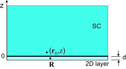
The Matsubara Green functions are
and
etc. We introduce the Nambu matrixes
and denote
the inverse operator in the superconductor. If needed, it can also include the impurity self energy. Neglecting the back-action of the thin 2D layer on the superconductor, we have for the superconducting Green function
Equations for the mixed Green functions can be written in the form
where
This gives
| (5) |
Equations for the Green functions in the layer can be written as
where the inverse operator in the layer is introduced,
| (6) |
Here the kinetic energy operator is
while is the shift of the bottom of the 2D conduction band measured from that in the superconductor.
We assume a site-to-site tunnelling which does not conserve momentum, , etc., where is real and does not depend on . Here selects an average value of a function at a distance of the order of inter-atomic scale near the surface. As a result,
| (8) |
where means that and .
The coordinate dependence of the Green functions has the form GorkovKopnin73
| (9) |
Here is the mean free path is the superconductor, is a unit vector, , and is the quasiclassical superconducting Green function integrated over the energy variable, Eq. (10),
| (10) |
which depends only on the direction of the momentum .
The self-energy in Eq. (8) oscillates as while the Green function contains where is close to the Fermi momentum in the 2D layer. If , the integral in Eq. (7) converges at where is the interatomic distance. Therefore, one can invoke the approximation
The first term in Eq. (9) diverges for , but it does not depend on the superconducting state. It is real and has the form of an effective potential. We can include it into the shift of the bottom of the conduction band or into the chemical potential assuming that already accounts for it. The remaining term for gives
| (11) |
Here we introduce the tunnelling rate where is the 3D density of states, is of the order of the area of the unit cell in the layer; the overall order of magnitude is . Angular brackets denote averaging over momentum directions. The quasiclassical Green function taken at the superconductor/2D-layer interface is the only characteristic which is needed in our model to account of the properties of the bulk superconductor. Since the quasiclassical function varies over distances of the order of superconducting coherence length, the exact atomic-scale boundary conditions at the interface for the microscopic wave functions are not critical for our model.
We write the final equation in 2D layer for the real-time Green functions making the analytical continuation of the Matsubara functions onto the real-frequency axis. We introduce the Keldysh matrixes
The equations become (the index is dropped)
| (12) |
where
III S/2D/S structure
III.1 Green functions

In this paper we restrict ourselves to stationary problems and put . In the following Sections we apply our model to the S/2D/S structures which are made of a ballistic 2D electron gas placed in a contact with bulk superconducting leads (S). One of the examples is shown in Fig. 2. A generic structure of this type consists of a layer of 2D electron gas which is infinite in direction and has boundaries at certain where . Transforming to the plane waves along the direction,
we observe that, as functions of for , the retarded Green functions and satisfy the set of 2 linear homogeneous second-order differential equations which follow from Eq. (12),
| (13) | |||
| (14) |
where is the chemical potential in the 2D gas measured from the bottom of the conduction band, , and
| (15) |
Eqs. (13), (14) have 4 independent solutions,
Using the standard method in the theory of differential equations, one can write the Green functions as sums
The functions are chosen such that the retarded Green functions are regular in the upper half-plane, . The coefficients do not depend on but can be functions of . We find from Eq. (12)
Let us define the vectors
and the matrix where
The upper index numerates columns, while the lower numerates rows. Equations take the form . The solution is
| (18) |
Here is the Wronskian and where is a minor of . The Wronskian is independent of coordinates.
III.2 Reflection coefficients
Consider structure shown in Fig. 2. The right superconductor has the phase while the left one has . The four independent functions needed for the Green functions can be constructed as follows. The first two wave functions inside the 2D layer contain waves incident from the left and reflected from the right boundary,
| (19) | |||||
| (20) | |||||
Here , while and are the components of the Fermi wave vector and Fermi velocity in the 2D gas, ; the particle and hole Nambu vectors are
The set of two other functions is obtained using reflection from the left boundary,
| (21) | |||||
| (22) | |||||
In the right induced-superconductivity region , the four functions satisfying Eqs. (13) - (14) are linear combinations of
The functions in the left superconducting region are obtained by replacing with and with . Note that the momentum in the induced-superconductivity region,
| (25) |
has the same Fermi-momentum projection on the coordinate as in the normal region. Thus the normal reflection at does not occur. The coherence factors are
| (26) |
Here
| (27) |
since . Moreover
The square roots are defined as analytic functions in the plane of complex with cuts from to and from to taken at the upper bank of the cut for . The usual BCS formulas are recovered if one uses such that the BCS gap is replaced with .
The boundary conditions require that at together with continuity of at . This yields
| (28) | |||||
| (29) | |||||
| (30) | |||||
| (31) |
where
Here we denote and , while
| (32) |
One can check that the Green functions defined according to Eq. (18) with the basis functions Eqs. (19)–(22) are regular in the upper half-plane of complex . For the coefficients satisfy
| (33) |
because there is no quasiparticle flux into the superconductor.
As in Ref. KM-etal-05 one can define an equivalent barrier hight associated with the end of the conduction layer,
| (34) |
such that the coefficients have their standard form BTK82 ; KMV2006
| (35) |
The limit corresponds to strong normal reflection, and , while . With this definition of effective barriers, the problems of the bound-state spectrum and of the supercurrent in many respects reduce to the corresponding problems in double-barrier superconductor/normal/superconductor (SINIS) structures.
Let us denote the energy at which the square root in Eq. (25) vanishes, i.e., at which defined by Eq. (27) turns to zero,
| (36) |
The energy is the induced gap in the 2D layer. For we have ; if one has . The induced gap as a function of is shown in Fig. 3. For a 2D gas in a direct contact with a superconductor, the induced gap was obtained in Ref.AVolkov95 .
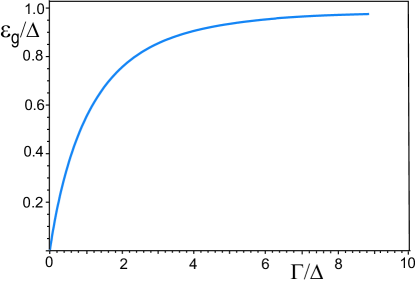
If , both the square root in Eq. (25) and are imaginary. The value is real and satisfies
| (37) |
For large we have ; the particles do not feel the dead end of the superconducting region, such that the normal reflection is absent, while . This limit is realized when where
is the coherence length of the induced superconductivity, is the Fermi velocity in the 2D system . The limit of long leads is rather hard to realize because is considerably longer than in a bulk superconductor. On the contrary, for short leads, , there exists only normal reflection, , and .
If both the phases and the coherence factors , are real, while is complex. The Andreev reflection vanishes while if .
III.3 Bound states. Supercurrent
Using the functions Eqs. (19) – (22) and Eqs. (28)–(31), we find the Wronskian
where , , while is the phase of the reflection coefficient , i.e., . The spectrum is determined by , which gives
| (38) |
where . This agrees with the previous calculations of Ref. KMV2006 for ballistic SINIS contacts. Here we concentrate on short contacts such that . Neglecting and keeping finite implies that one has to assume .
If the energy is above the induced gap, , the combination , as well as and are real. For energies below the induced gap, , the barrier strength , Eq. (34), is real, while . Therefore, Eq. (38) yields for the bound state energy
| (39) |
where
| (40) | |||||
| (41) |
Equation (40) goes into Eq. (41) if one continues analytically the phase difference as a function of around the induced gap .
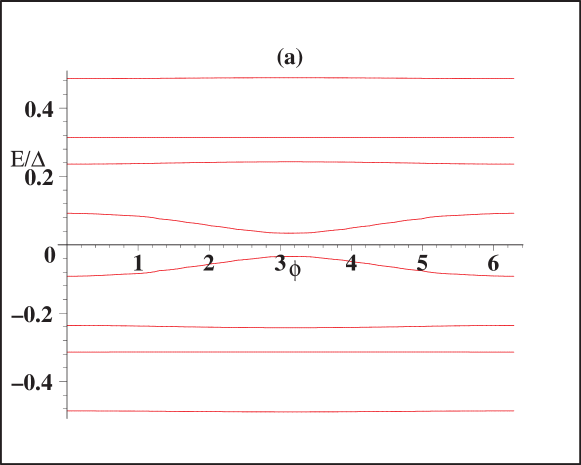
For energies below qusiparticles cannot escape into the superconductors and form the bound states as a result of two processes: the Andreev reflection at the boundary between the normal region and the region with induced-superconductivity plus the normal reflection at the ends of the 2D layer. The spectrum is determined by Eq. (39); it consists of a series of levels for each and spaced with a distance and filling the interval . The lowest energy level lies below the induced gap if . For short leads, , the energies are close to the levels of geometrical quantization in a potential well of length , i.e., they satisfy . If , there is only one bound state with energy .
The supercurrent isBeenakker91
| (42) |
Here
is the Sharvin conductance of the contact, is the conductance quantum, is the Fermi momentum in the layer, and is the normal density of states in the 2D gas. The conductance is proportional to the number of modes in the 2D channel of width in the direction. The sum collects all bound states with energies for given . The continuum states with give the contribution proportional to the length and can thus be neglected.
III.3.1 Short leads
Consider the case of short leads, for . This is the most practical situation in the experimental devices. If , there is a series of bound states with energies . As discussed above, they are close to the levels of dimensional quantization. Putting we observe that where
| (43) |
and
| (44) |
which follows from Eqs. (39), (40). Equation (43) gives
| (45) |
Here is the smallest root, , of Eq. (43). This solution holds as long as , i.e., for all states with . It also holds for the lowest energy state, as long as the level is not very close to the resonance, .
Close to the resonance, , the lowest level can also be obtained by expanding the sine functions in Eqs. (40), (41). Putting we find
| (46) | |||||
where . Close to the resonance, ,
| (47) |
This goes over into Eqs. (45), (44) when . The typical spectrum is shown in Fig. 4(a).
If the leads are very short, then there exists only one level. Except for a very narrow vicinity of resonance, one has , thus the level is close to the superconducting gap ,
| (48) |
To calculate the supercurrent Eq. (42) we integrate the contribution from each level over the incident angle defined according to . Since the resonance form of the level, Eq. (47), holds only in a very narrow region of angles, its contribution to the current is small. The current is thus mostly determined by the off-resonance levels, Eqs. (45), (44), or (48) with . For , there is a series of levels defined by Eqs. (45), (44). The current is
| (49) | |||||
where
Due to a large argument in , the level oscillates rapidly assuming values within the interval many times as the incident angle varies from to . Let us consider a function of the rapidly oscillating variable and a slow variable and define the average function where the integral is taken over the full variation range of putting . Since the range corresponds to a small variation , one can keep the slow variable constant during integration over ,
The integral of the rapid function can now be replaced with the integral of the average function .
For low temperatures, one can simplify the expression (49) for the current. We note that for the integral in diverges logarithmically at ; it should be cut off when , i.e., at . Therefore, within the logarithmic accuracy,
For the integral diverges logarithmically at . At the lower limit, , the function under the integral should be replaced with that containing the resonance level taken from Eq. (47). Therefore, we find
where
Here and . For low temperatures,
It is independent of within the logarithmic accuracy. Performing the summation we find for
| (50) |
The current-phase relation is sinusoidal; this corresponds to the limit of low transparency junctions realized in short-lead contacts with . The supercurrent increases with lowering the temperature and saturates for . For temperatures higher than , the logarithm decreases to a value of order unity, and our approximation breaks down. Note that the current-phase relation, Eq. (50), is similar to that obtained for a double barrier SINIS structure with resonant transmission (see, e.g., Ref. galaktionov, ).
If the leads are very short, , there exists only one level, Eq. (46). The estimates show that, within the logarithmic approximation, the current is dominated by the spectrum close to the resonance, Eq. (47), and still has the form of Eq. (50).
III.3.2 Long leads
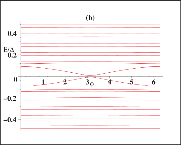
Here we again restrict ourselves to the limit . For the contact with long leads, the spectrum consists of one level with satisfying Eqs. (39), (41) and a series of levels with satisfying Eqs. (39), (40). Typical spectrum of bound states for a contact with long leads is plotted in Fig. 4(b).
For we find from Eqs. (39), (41)
| (51) |
where . If we have thus , i.e., this energy state is as in a ballistic junction with a gap ,
This level gives the usual expression for the supercurrent as in a ballistic contactKulik78 with an induced gap AVolkov95 ,
| (52) |
One also needs to consider the contribution of levels with energies above the induced gap. For Eqs. (39) and (40) yield where and
| (53) |
Here we denote . Expanding in we find . For we have
The terms in proportional to disappear. The number of terms in the sum is , being determined by the condition . Therefore, the sum over the states with is of the order of , and can thus be neglected. As a result, Eq. (52) is the full expression for supercurrent through a contact with long leads. In this sense, the contact with long leads behaves as a contact without normal reflection, , when the bound states would only exist for . This limit was considered in Ref.AVolkov95 .
IV The I-V curve in a 2D/S junction

The results obtained in the previous section can be used to describe the transport in a 2D/S junction shown in Fig. 5. The junction consists of a semi-infinite normal 2D layer a part of which (with a length L) is covered by a bulk superconducting lead. The current through such contact can be written in terms of reflection coefficients obtained in Sec. III.2. Using the results of Ref. BTK82 , we have
where is the Fermi function. For the differential conductance is
| (54) |
where .
IV.1 Long leads. Andreev reflection
Consider the case such that the length is longer than the electronic mean free path, . In this limit one can neglect the effect of the dead end and assume that .
For we have zero normal reflection amplitude and the Andreev reflection coefficient which is independent of . For the Andreev reflection coefficients becomes
For we have
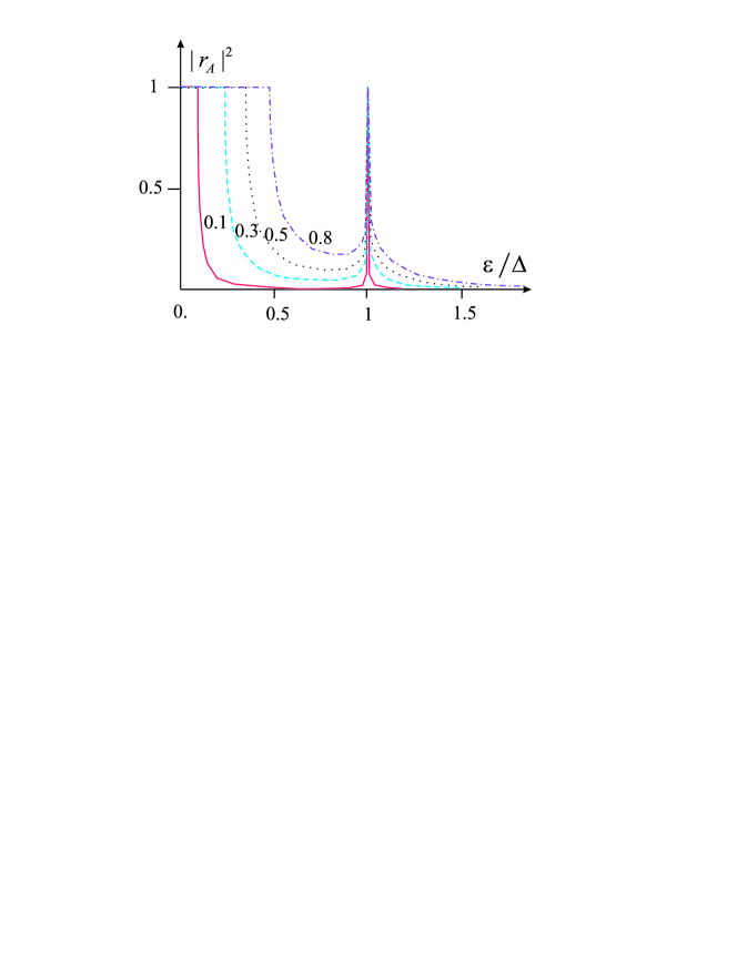
If , one has and . If we also have . If then for we have . Since the Andreev reflection does not depend on , Eq. (54) yields for
where . The Andreev reflection coefficient for a long contact is shown in Fig. 6. The limit of a long contact with zero normal reflection was considered in Ref. Fagas-etal-05 using a direct-contact model.
IV.2 Finite-length leads. Oscillations of the resistance
Here we discuss contacts with finite-length leads in the weak coupling limit, . For when quasiparticles cannot escape into the leads, Eq. (33) gives . Equation (54) yields
In the low-voltage region, , we have while is real. Therefore,
In the weak coupling case and
The differential conductance becomes
It does not depend on voltage. For short leads , the conductance is determined by the incident angles close to where the Andreev reflection is of the order of unity. For long leads the Andreev reflection is complete as in the previous Section IV.1.
For energies , the Andreev coefficient is
If the energy is not very close to the superconducting gap, , we have , while . Therefore
and . Therefore, for ,
where . The conductance exhibits oscillations as a function of the bias voltage due to the geometrical quantization.
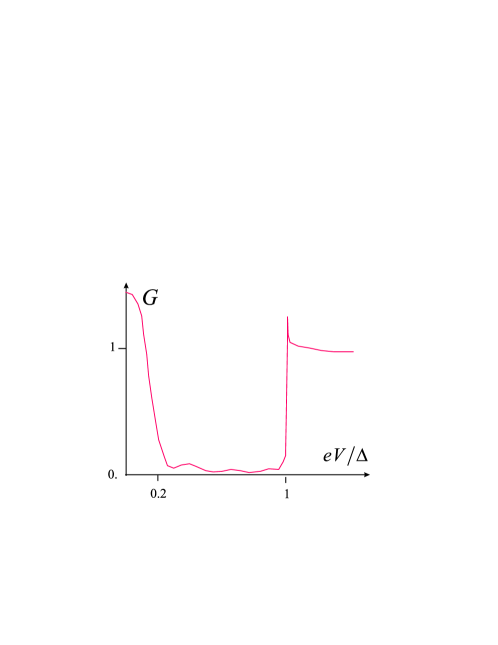
Consider now the energies . Not very close to the gap edge the Andreev reflection is small, while
For short contacts we find
| (55) |
Region close to the gap edge, needs a special consideration. Here , so that the normal reflection vanishes while the Andreev reflection grows up to , and the conductance has a sharp peak as in the case of long contacts considered in Sec. IV.1. The differential conductance is plotted in Fig. 7.
As was mentioned in Sec. III.2, short leads are equivalent to the limit of low transmission tunnel contact. The differential conductance Eq. (55) at voltages is proportional to the superconducting density of states, as it is usually the case for tunnel contacts. However, in addition to the peak at the superconducting gap edge, the differential conductance has a low-energy peak which characterizes the induced superconducting gap in the 2D layer. In the voltage interval , the conductance oscillates as a function of voltage due to the geometrical quantization in the regions where the leads overlap with the 2D layer. The contacts with long leads, , for have an exponentially small normal reflection due to almost complete escape of quasiparticles into the superconductors, and thus their conductance coincides with that obtained in Sec. IV.1.
V Discussion
We formulate the approach which can be used for spatially inhomogeneous and/or time-dependent problems associated with the induced superconductivity in low dimensional electronic systems including a 2D electron gas, graphene layer, etc. This approach is based on the so-called Fano–Anderson model which describes the decay of a resonance state coupled to a continuum FanoAnderson . We consider a 2D system placed in a contact with a bulk superconductor and use the tunnel approximation for coupling between the superconductor and the 2D electron layer in a way similar to that used in Refs. Shiba ; ArseevVolkov91 for impurities in a superconductor. We consider two particular examples of junctions made of a ballistic 2D electron gas placed under the superconducting electrodes of a finite length. For the case of a short symmetric S/2D/S junction we find the bound states localized in the junction and calculate the supercurrent as a function of the lead length. Next we consider the 2D/S junction and find the IV curve for various lead lengths. We show that the differential conductance as a function of the bias voltage exhibits peaks which correspond to the induced and bulk superconducting gaps. The differential conductance also shows oscillations as a function of voltage due to geometrical quantization in the regions with the induced superconductivity.
Acknowledgements.
We thank A. Ioselevich and S. Sharov for stimulating discussions. This work was supported in part by the Academy of Finland, Centers of excellence program 2006–2011, by the Russian Foundation for Basic Research under grant 09-02-00573-a, by Russian Agency of Education under the Federal Program “Scientific and educational personnel of innovative Russia in 2009-2013” and by the Program “Quantum Physics of Condensed Matter” of the Russian Academy of Sciences.References
- (1) K. S. Novoselov, A. K. Geim, S. V. Morozov, D. Jiang, M. I. Katsnelson, I. V. Grigorieva, S. V. Dubonos, and A. A. Firsov, Nature 438, 197 (2005).
- (2) C.W.J. Beenakker, Phys. Rev. Lett. 97, 067007 (2006); M. Titov and C.W.J. Beenakker, Phys. Rev. B 74, 041401 (2006).
- (3) J. Tworzydło, B. Trauzettel, M. Titov, A. Rycerz, and C.W.J. Beenakker, Phys. Rev. Lett. 96, 246802 (2006).
- (4) J.C. Cuevas and A. Levy Yeyati, Phys. Rev. B 74, 180501 (2006).
- (5) P. Burset, A. Levy Yeyati, and Martín-Rodero, Phys. Rev. B 77, 205425 (2008).
- (6) P. Burset, W. Herrera, and A. Levy Yeyati, Phys. Rev. B 80, 041402 (2009).
- (7) A.M. Black-Schaffer and S. Doniach, Phys. Rev. B 78, 024504 (2008).
- (8) J. Linder, A.M. Black-Schaffer, T. Yokoyama, S. Doniach, and A. Sudbø, Phys. Rev. B 80, 094522 (2009).
- (9) D. Rainis, F. Taddei, F. Dolcini, M. Polini, and R. Fazio, Phys. Rev. B 79, 115131 (2009).
- (10) A.F. Volkov, P.H.C. Magnée, B.J. van Wees, and T.M. Klapwijk, Physica C 242, 261 (1995).
- (11) G. Fagas, G. Tkachov, A. Pfund, and K. Richter, Phys. Rev. B, 71, 224510 (2005).
- (12) H. Shiba, Progr. Theor. Phys. 50, 50 (1973).
- (13) P.I. Arseev and B.A. Volkov, Zh. Eksp. Teor Fiz. 100, 334 (1991) [Sov. Phys. JETP 73, 185 (1991)].
- (14) U. Fano, Phys. Rev. 124, 1866 (1961); P.W. Andreson, Rev. 164, 41 (1961).
- (15) L.P. Gorkov and N.B. Kopnin, ZhETF, 64, 356 (1973) [Sov.Phys. JETP 37, 183 (1973)].
- (16) N.B. Kopnin, A.S. Melnikov, V.I. Pozdnyakova, D.A. Ryzhov, I.A. Shereshevskii, and V.M. Vinokur, Phys. Rev. Lett. 95, 197002 (2005).
- (17) G.E. Blonder, M. Tinkham, and T.M. Klapwijk, Phys. Rev. B 25, 4515 (1982).
- (18) N.B. Kopnin, A.S. Mel’nikov, and V.M. Vinokur, Phys.Rev. Lett. 96, 146802 (2006).
- (19) C.W.J. Beenakker and H. van Houten, Phys. Rev. Lett. 66, 3056 (1991).
- (20) A.V. Galaktionov and A.D.Zaikin, Phys. Rev. B 65, 184507 (2002).
- (21) I.O Kulik and A.N. Omel’yanchuk, Fiz. Nizk. Temp. 4, 296 (1978) [Sov. J. Low Temp. Phys. 4, 142 (1978)]