Evidence for Helical Edge Modes in Inverted InAs/GaSb Quantum Wells
Abstract
We present an experimental study of low temperature electronic transport in the hybridization gap of inverted InAs/GaSb composite quantum wells. Electrostatic gate is used to push the Fermi level into the gap regime, where the conductance as a function of sample length and width is measured. Our analysis shows strong evidence for the existence of helical edge modes proposed by Liu et al [Phys. Rev. Lett., 100, 236601 (2008)]. Edge modes persist inspite of sizable bulk conduction and show only a weak magnetic field dependence - a direct consequence of gap opening away from zone center.
Topological insulators (TI) are a novel phase of matter,(1, 1, 2) originally predicted to manifest in 2D structures(3, 3) as a superposition of two quantum Hall systems,(4, 4) where the role of the spin-dependent magnetic field is played by the spin-orbital interactions. In extension of the paradigm to 3D, TI surfaces emerge as "half-graphene" with an odd number of Dirac cones.(5, 5) In 2D, the TI phase is also known as quantum spin Hall insulator (QSHI) and is characterized by an energy gap in the bulk and topologically protected helical edge states. Quantized conductance, taken as the evidence for the QSHI phase, has been experimentally observed in the inverted HgTe/CdTe quantum wells (QWs).(6, 6, 7) Liu et al(8, 8) have proposed that QSHI should arise in another semiconductor system, the hybridized InAs/GaSb QWs, where a rich phase diagram including band insulator and QSHI can be continuously tuned via gate voltages. Here we present a systematic transport study of high quality InAs/GaSb devices tuned into the QSHI state, where we observe slowly-propagating helical edge modes that are largely immune to a conductive bulk. Exploring this system should have a far-reaching impact, since InAs makes a good interface with superconductors,(9, 9) a prerequisite for fabricating TI/superconductor hybrid structures;(10, 10) the latter are predicted to host exotic Majorana fermion modes and are viable for fault-tolerant quantum computing.
A common characteristic to all TIs is band inversion, which in InAs/GaSb is achieved by tuning energy levels in two neighboring electron and hole QWs. Hybridization of electron-hole bands leads to a gap opening, which has been experimentally well established, albeit always with a non-zero residual conductivity.(11, 11, 12) In an early theoretical study,(13, 13) the origin of the residual conductivity has been ascribed to the level-broadening due to scattering. Interestingly, in the “clean limit”, the gap conductivity is finite, yet independent of scattering parameters, such as sample mobility. Motivated by the QSHI proposal,(8, 8) Knez et al(14, 14) revisited the issue of gap conduction in micro-size samples. They found a bulk conductivity on the order of , consistent with(13, 13) and a few times larger than the expected contribution from the edge. Nevertheless, bulk conductivity diminishes as the band inversion is reduced,(14, 14) promoting the QSHI. In this Letter we study the length and width dependence of conductance in the hybridization regime and find direct evidence for the existence of helical edge modes proposed by Liu et al.(8, 8) Surprisingly, edge modes persist alongside the conductive bulk and show only weak magnetic field dependence. This apparent decoupling between the edge and bulk is a direct consequence of gap opening away from the zone center, which leads to a large disparity in Fermi wave-vectors between bulk and edge states, and results in a qualitatively different QSHI phase than in HgTe/CdTe where the gap opens at the zone center.
InAs/GaSb has a broken gap band alignment allowing for the coexistence of closely separated electron (in InAs) and hole (in GaSb) two-dimensional gases and confined by neighboring AlSb barriers as shown in Fig. 1a.(15, 15) For wider wells the band structure is inverted with the ground conduction subband (E1) lower than the ground heavy-hole subband (H1). Relative position of the E1 and H1 bands can be tuned by an external electric field(15, 15) applied via front and back gates. In inverted regime the E1 and H1 bands anti-cross for some finite wave-vector , where electron and hole densities are approximately matched, . Due to the tunneling between the wells, electron and hole states are mixed and a hybridization gap Δ opens in the otherwise semi-metallic band dispersion as shown in Fig. 1b.(15, 15) Matching of the inverted bands to the corresponding vacuum states leads to an inevitable gap closing at the sample perimeter and results in linearly dispersing edge modes.(8, 8) Time reversal symmetry of the governing Hamiltonian requires the edge modes to be helical, i.e. counter-propagating spin up and spin down channels with conserved helicity. As a result, particles on time-reversed paths around a non-magnetic impurity in the helical edge destructively interfere, resulting in zero backscattering probability.(2, 2) For Fermi energy in the gap, expected edge conductance in a six-terminal configuration for mesoscopic samples will be .(7, 7) Here we use a four-terminal configuration where expected edge conductance is doubled to .
Longer samples can be modeled by inserting phase breaking probes(16, 16) and applying the Landauer-Buttiker formula yielding four-terminal conductance as:
| (1) |
where is the phase coherence length and is the device length. Thus, for macroscopic QSH samples the edge contribution to the conductance will be negligible. Note that due to the level broadening the hybridization gap exhibits a sizable bulk conductivity, which for small level broadening , scales as ,(13, 13, 14) where is the relative separation between H1 and E1 bands. While helical edge transport manifests itself only in the mesoscopic regime, macroscopic samples can be used as an important diagnostic of bulk gap conduction, allowing us to separate edge from bulk contributions which coexist in mesoscopic samples.


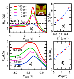
The experiments are performed on high quality 125Å InAs/50Å GaSb quantum wells, in inverted regime. Sample fabrication and measurement details are given in Ref. (14, 14, 22). Here the data were taken from eight devices made from the same wafer. Fig. 1c shows longitudinal resistance (in red) vs. front gate bias of a Hall bar with width and length , at , As is swept from to , is pushed from purely electron to two-carrier hole dominated regime. When , a strong resistance peak of is observed, which for this macroscopic sample reflects only the bulk transport, with bulk gap conductivity of , where . Entry into hybridization gap is also signaled by non-linearity in (taken at ) shown in Fig. 1c in blue. Negative values of indicate hole-dominated regime although in two-carrier regime direct correspondence to carrier density no longer exists. The size of the mini-gap can be determined from the relative position in of the resistance dip, which corresponds to the Van Hove singularity at the gap edge, and the resistance peak which corresponds to the middle of the gap:(11, 11, 14) where is the rate of carrier density change with and is density of states, with carrier masses and (in units of free electron mass),(11, 11) giving . From the minimum in which corresponds to an anti-crossing density of , we can estimate , where is the reduced mass. The expected bulk conductivity is then(13, 13) , consistent with the observed value.

Fig. 2a shows resistance peaks for and with . The resistance peak of the device is used to estimate the bulk gap resistance . Surprisingly, a parallel combination of and the expected edge resistance gives a resistance value of (dashed black line in Fig. 2a) which is just slightly above the measured valued of for the device. A plot of the gap conductance vs. in Fig. 2b can be fitted with Eq. 1, obtaining and giving further evidence for the existence of helical edge conduction channels in mesoscopic samples. In fact, the difference in conductance between the mesoscopic and the macroscopic samples is just slightly above , as expected for helical edge modes.(17, 17)
In width dependence experiment we fix , while is varied from to . While the resistance peaks shown in Fig. 2c increase as is decreased, plot of vs. in Fig. 2d reveals a reasonably linear relationship with an intercept of the linear fit of , in support of helical edge transport. As an important check, the slope of the same fit gives a bulk conductivity of which is consistent with the value estimated earlier. Thus, both the length and the width dependence of the gap conductance consistently confirm the existence of helical edge channels in inverted InAs/GaSb QWs.

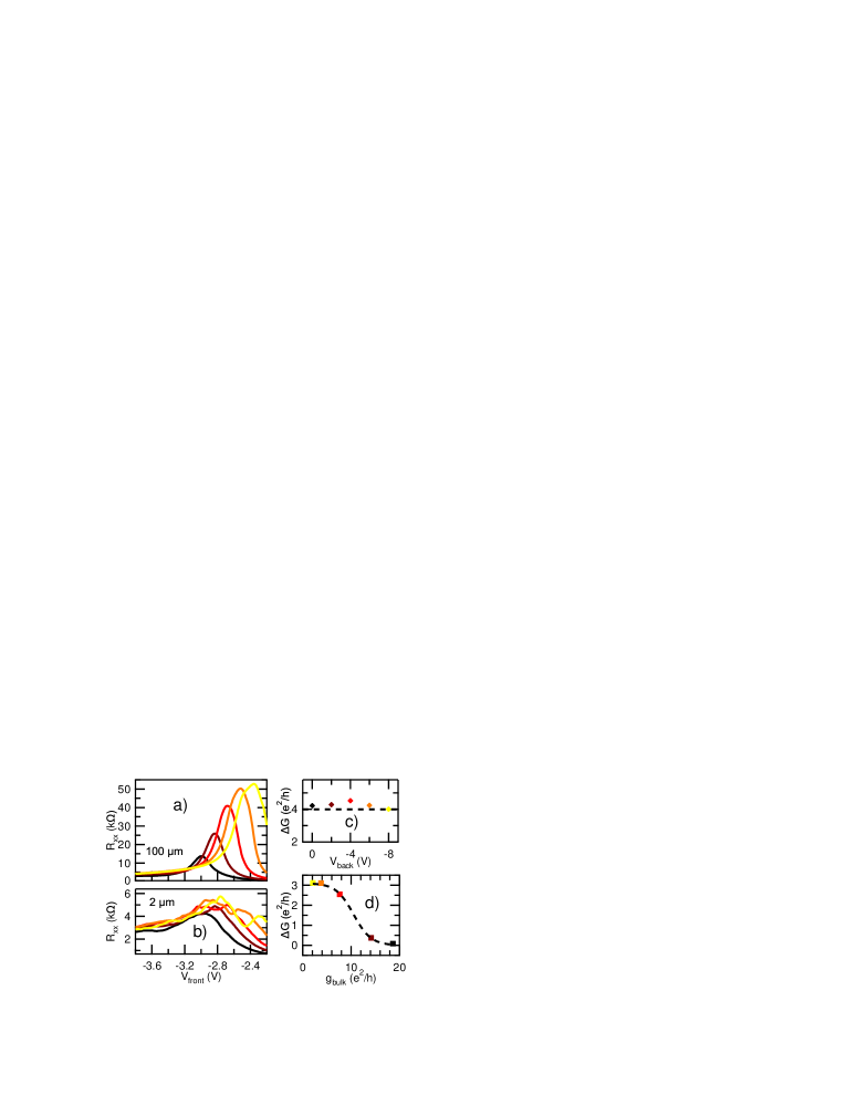
Using the anti-crossing point can be tuned to lower values, thereby supressing . Fig. 3 shows vs with varied in steps from to for devices of in a) and in b), in both cases. As is tuned to more negative values, the separation between the bands is reduced, and the resistance peaks of the sample increase from at , to at . On the other hand, the resistance peaks of the mesoscopic sample increase only slightly, from at , to at . In fact, the conductance difference between mesoscopic and macroscopic samples, stays around for all values of , as shown in Fig. 3c, accounting for the helical edge transport.
Data presented in Fig. 3a may suggest that edge conduction is completely independent of gap bulk conductivity, . However, this is valid only in the regime of low . Note that in Fig. 3a . Using bias cooling technique,(14, 14) the system can be pushed deeper into the inverted regime, i.e. a larger can be obtained, so that at , , while at , . In this case, the edge conductance, i.e. , goes from for large bulk conductivity of to about as the bulk conductivity is reduced to , as shown in Fig. 3d. The cut-off bulk conductivity at which edge conduction “activates” can be estimated to .
The apparent resilience of edge conduction to bulk transport is quite unexpected, considering that a conductive bulk would allow edge electrons to tunnel from one side to another, resulting in inter-edge scattering and a reduced edge conductance.(18, 18, 19) However, the inter-edge tunneling probability may be significantly reduced by a large Fermi wave-vector mismatch. The bulk gap states are inherited from the non-hybridized band structure and have a Fermi wave-vector equal to while edge modes, for situated in the middle of the gap, have . Thus, due to edge modes are totally reflected from bulk states. In fact, the tunneling probability for the edge electrons will be proportional to the edge-bulk transmission probability, which scales as , as well as the bulk transmission, which scales as bulk conductivity, i.e. as . Hence, the overall inter-edge tunneling probability will decrease as is reduced, which is in a qualitative agreement with data in Fig. 3d. Furthermore, due to the low Fermi velocity of edge states , relativistic effects of Rashba spin-orbital interaction will be small, and electron spins are expected to be aligned along the growth axis, reducing inter-edge tunneling due to Pauli exclusion.(20, 20)
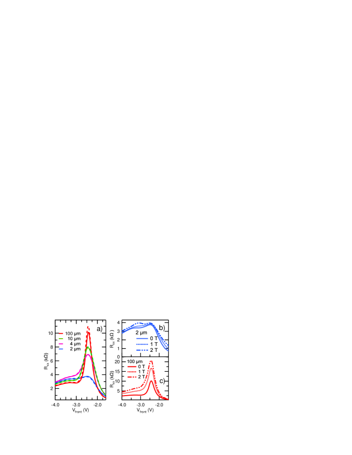
The resistance peaks of mesoscopic samples show only a weak dependence on in-plane and perpendicular magnetic fields, as shown in Fig. 4a and 4b respectively, while macroscopic samples show a much stronger dependence. At first glance, this appears to be in contrast to the strong field dependence reported for HgTe/CdTe QWs(7, 7). However, even in HgTe a strong magnetic field dependence has never been observed in the smallest micron size samples,(20, 20) but only in longer samples.(7, 7) In fact, it has been shown theoretically by Maciejko et al(21, 21) that the magnetic field decay of edge modes depends sensitively on disorder strength, with pronounced cusp-like features of magneto-conductance occurring only when the disorder strength is larger than the gap. The underlying physical picture is that by providing the states in the bulk by large disorder, edge electrons can diffuse into the bulk enclosing larger amounts of flux whose accumulation destroys destructive interference of backscattering paths, resulting in a linear decay of conductance with . In the case of HgTe, large disorder was provided by in-homogenous gating, which is more pronounced for longer devices.(7, 7)
In InAs/GaSb edge states are effectively decoupled from the bulk and the above flux effect plays a lesser role, resulting in a weaker magnetic field dependence of edge modes. However, the decay of bulk conductivity itself with magnetic field may not necessarily be weak due to the localization of non-hybridized carriers. This localization is more pronounced for longer samples, which have stronger disorder. Thus, longer samples are expected to show stronger magnetic field dependence, as experimentally observed. We note here that localization at high magnetic fields results in a dramatic re-entrant quantum Hall effect.(22, 22) Such re-entrant behavior is a signature mark of topologically distinct band structure,(7, 7) and its observation validates the topological origin of helical edge modes at zero magnetic field.
In conclusion, inverted InAs/GaSb CQWs in hybridization regime host slowly-propagating helical edge modes which persist despite conductive bulk and show only weak magnetic field dependence. This remarkable property can be qualitatively explained by gap opening away from Brillouin zone center, unlike in HgTe where the gap opens at . Demonstrated band structure tunability and good interface to superconductors make this QSHI system a promising candidate in realization of exotic Majorana modes.
The work at Rice was supported by Rice Faculty Initiative Fund, Hackerman Advanced Research Program grant 003604-0062-2009, Welch Foundation grant C-1682, and NSF grant DMR-0706634. I.K. acknowledges partial support from M. W. Keck Scholar. We thank S.-C. Zhang for bringing our attention to Ref. (8, 8), S.-C. Zhang, X.-L. Qi, C. Liu, J. Maciejko, and M. Konig for many helpful discussions.
References
- (1) M.Z. Hasan and C.L. Kane, Rev. Mod. Phys. 82, 3045 (2010).
- (2) X.-L. Qi and S.-C. Zhang, arXiv:1008.2026 (2010).
- (3) C.L. Kane and E.J. Mele, Phys. Rev. Lett. 95, 226801 (2005).
- (4) B.A. Bernevig, S. C. Zhang, Phys. Rev. Lett. 96, 106802 (2006).
- (5) L. Fu, C.L. Kane and E.J. Mele, Phys. Rev. Lett. 98, 106803 (2007).
- (6) B. A. Bernevig, T. L. Hughes, S.-C. Zhang, Science 314, 1757-1761 (2006).
- (7) M. Konig, S. Wiedmann, C. Brune, A. Roth, H. Buhmann, L. W. Molenkamp, X.-L. Qi, and S.-C. Zhang, Science 318, 766-770 (2007).
- (8) C. Liu, T.L. Hughes, X.-L. Qi, K. Wang, and S.-C. Zhang, Phys. Rev. Lett., 100, 236601 (2008).
- (9) C. Nguyen, J. Werking, H. Kroemer and E.L. Hu, Appl. Phys. Lett. 57, 87 (1990).
- (10) L. Fu, and C. L. Kane, Phys. Rev. Lett. 100, 096407, (2008).
- (11) M. Yang, C. Yang, B. Bennett, and B. Shanabrook, Phys. Rev. Lett., 78, 4613-4616 (1997).
- (12) L. Cooper, N. Patel, V. Drouot, E. Linfield, D. Ritchie, and M. Pepper, Phys. Rev. B, 57, 11915-11918 (1998).
- (13) Y. Naveh and B. Laikhtman, Euro. Phys. Lett., 55, 545-551 (2001).
- (14) I. Knez, R.R. Du, and G. Sullivan, Phys. Rev. B 81, 201301(R) (2010).
- (15) Y. Naveh and B. Laikhtman, Appl. Phys. Lett. 66, 1980-1982 (1995).
- (16) See e.g., S. Datta, Electronic Transport in Mesoscopic Systems, Cambridge, 1995.
- (17) The small difference may come from a logarithmic correction to bulk conductivity due to localization which goes as , where is the mean free path. See e.g., E. Abrahams, P. W. Anderson, D. C. Licciardello, and T. V. Ramakrishnan, Phys. Rev. Lett. 42, 673 (1979). However, the logarithmic correction accounts only for the fraction of the difference in conductance between mesocopic and macroscopic samples, i.e. compared to a total difference of .
- (18) B. Zhou, H. –Z. Lu, R.–L Chu, S. –Q. Shen and Q. Niu, Phys. Rev. Lett. 101, 246807 (2008).
- (19) J.I. Väyrynen and T. Ojanen, Phys. Rev. Lett. 106, 076803 (2011).
- (20) M. Konig, Ph.D. Thesis, Wurzburg University (2007); private communications.
- (21) J. Maciejko, X.-L. Qi and S.-C. Zhang, Phys. Rev. B 82, 155310 (2010).
- (22) I. Knez, R.R. Du and G. Sullivan, to be published.