From laterally modulated two-dimensional electron gas towards artificial graphene
Abstract
Cyclotron resonance has been measured in far-infrared transmission of GaAs/AlxGa1-xAs heterostructures with an etched hexagonal lateral superlattice. Non-linear dependence of the resonance position on magnetic field was observed as well as its splitting into several modes. Our explanation, based on a perturbative calculation, describes the observed phenomena as a weak effect of the lateral potential on the two-dimensional electron gas. Using this approach, we found a correlation between parameters of the lateral patterning and the created effective potential and obtain thus insights on how the electronic miniband structure has been tuned. The miniband dispersion was calculated using a simplified model and allowed us to formulate four basic criteria that have to be satisfied to reach graphene-like physics in such systems.
pacs:
73.22.Pr, 73.21.Cd, 78.67.PtI Introduction
The range of approaches to explore Dirac fermions in condensed-matter physics has recently been extended beyond natural grapheneNovoselov et al. (2005); Zhang et al. (2005); Geim and Novoselov (2007) to artificially created lattices whose properties such as inter-site coupling or lattice constant can be tuned. One approach here is to subject gas of ultracold atoms to a honeycomb optical latticeGrynberg et al. (1993) giving rise to Dirac cones in dispersion relations.Zhu et al. (2007); Wunsch et al. (2008) The same has been proposed for lithographically patterned two-dimensional electron gases (2DEGs) in semiconductor heterostructuresPark et al. (2008); Park and Louie (2009); Gibertini et al. (2009) as shown in Fig. 1. Apart from studying the Dirac fermions on their own, an appealing perspective in such semiconductor-based systems would be to fabricate various proof-of-principle electronic devices originally proposed for natural graphene,Dubois, S. M.-M. et al. (2009) for instance filters and valves,Rycerz et al. (2007) Veselago lenses,Cheianov et al. (2007) or splittersGarcia-Pomar et al. (2008). The electron-beam lithography used to define the artificial honeycomb crystal potential, dubbed artificial graphene (AG),Gibertini et al. (2009) allows for much easier control over the device details such as the edge geometry, additional or missing “atoms” than what would require an atom-by-atom manipulationEigler:1990_a in the case of natural graphene.
The subject of this paper, fabrication and theoretical description of AG, represents a special case of lateral semiconductor superlattices (SLs) intensively studied especially in the nineties. The body of widely explored phenomena can be roughly divided into two classes: classical and quantum-mechanical. Magneto-plasmons in far-infrared transmissionKern et al. (1991) and commensurability oscillationsWeiss et al. (1989) in a modulated 2DEG can be largely explained without invoking quantum mechanics.Mikhailov (1996); Beenakker (1989) On the other hand, SLs under strong magnetic fields, which leads to the magnetic breakdown,Středa and MacDonald (1990); Gvozdikov:2007_a as well as other more complex systemsAlbrecht et al. (1999); Olszewski et al. (2004); Gvozdikov:2007_b require quantum-mechanical ingredients (Bohr-Sommerfeld quantization and tunneling between semiclassical orbits).

In this context, the Dirac cone in the AG spectrum is a delicate quantum-mechanical feature just as the Hofstadter butterflyHofstadter (1976) — Landau bands emerging when quanta of magnetic flux pierce elementary cells of a square SL.Geisler et al. (2004); Pfannkuche:1992_a Despite promising recent progress,Gibertini et al. (2009); De Simoni et al. (2010); Singha et al. (2011) a clear-cut evidence of Dirac fermions in AG has not yet been found. Most likely, such an evidence can be provided in a magneto-transport or magneto-optical experiment by observing half-integer quantum Hall effect,Novoselov et al. (2005); Zhang et al. (2005) or the unique scaling in the optical response due to inter-Landau level (inter-LL) transitions.Sadowski et al. (2006); Jiang et al. (2007); Deacon et al. (2007) More careful engineering of AG structures is likely needed to realize these experiments.
In this paper, we explore the concept of artificial graphene both experimentally and theoretically. We use a simplified model of AG to formulate four straightforward criteria that must be fulfilled to achieve graphene-like physics in conventional 2D semiconductor heterostructures. Among these criteria, we focus on formation of a suitable miniband structure, explain how it is related to the modulation potential amplitude and show how this quantity can be measured in far-infrared magnetotransmission. Although the Dirac fermion physics in modulated semiconductor heterostructures has not been detected so far (including the experiments presented here), we conclude that simultaneous fulfilment of all the four criteria should be technologically feasible.
II Theory
To arrive at transparent conditions necessary for the realization of Dirac fermions in the SL miniband structure, we use a maximally simplified AG model which is effectively single-parametric.note1 The modulation potential , shown at Fig. 1(a) is taken as a sum of three cosine functions
| (1) |
where , , are the basis vectors in reciprocal space, is the distance between two maxima of and is the potential amplitude. Let us note that has to be positive to obtain a honeycomb structure rather than a trigonal one. The Hamiltonian in basis of plane waves,
| (2) |
is a matrix whose diagonal and off-diagonal matrix elements stand in a ratio determined by , and the electron effective mass (in GaAs, of the electron vacuum mass ; is the 2D momentum operator). Except for an overall scaling, eigenvalues of the matrix depend on a single dimensionless parameter
| (3) |
This parameter is, up to a factor of the order of unity, equal to the ratio between and the kinetic energy of a free electron () at the -point of the Brillouin zone.
Depending on , we obtain miniband spectra that continuously vary from the free 2DEG, through nearly-free and more tight-binding-like models, up to nearly flat bands that correspond to practically isolated (artificial) atoms. This is illustrated in Fig. 2, where we plot miniband structure for four different values of . In Fig. 2a, we plot the parabolic dispersion of a free electron () folded into the newly created Brillouin zone and then follow the evolution of the miniband structure with increasing , namely for , 0.9 and 4. The present Dirac cones are marked by vertical arrows and their pseudorelativistic character has been confirmed by analysing the corresponding wavefunctions.note2
Importantly, more than one Dirac cone appears within the seven lowest lying minibands shown in Fig. 2. This fact, to the best of our knowledge so far not mentioned in literature, may significantly simplify the quest for pseudorelativistic physics as we discuss below. The Fermi velocity corresponding to the lower and upper Dirac cone for the modulation strength (Fig. 2c) is roughly and m.s-1, respectively. The expected Fermi velocity in AG is thus more than order of magnitude lower as compared to natural graphene, where values around m.s-1 are reported.Novoselov et al. (2005) Another important characteristics of the created Dirac cones is their width in energy . A closer inspection of Fig. 2 reveals that we always get the smaller than and also that strongly depends on . The typical width of Dirac cones, , is dominantly given by two factors: the size of the Brillouin zone (i.e. the lattice constant ) and the effective mass of the employed semiconductor system (which defines the kinetic energy ).
Now we formulate four simple criteria which have to be fulfilled to achieve Dirac-like AG physics in hexagonally patterned heterostructures. Unless stated otherwise, we always consider lattice period nm and the effective mass of electrons in GaAs , which match to the samples explored experimentally below.

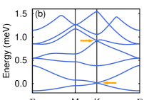
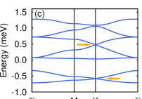

(i) Suitable miniband structure: The effective strength of the modulation has to be tuned to get well-separated and well-developed Dirac cones. Consistently with our calculations in Fig. 2, the range ensures that the Dirac cones do not overlap with other minibands, as is the case of low in Fig. 2b, and also the cones are not significantly flattened, which gradually happens for towards the limit of isolated “atoms”. If we strictly limit ourselves to the upper Dirac cone, the effective strengths somewhat exceeding 4 are still acceptable. Let us note that the chosen range of corresponds to the potential modulation that ranges from 0.6 to .
(ii) Fermi level positioning and/or carrier density: The Fermi level has to be located in the vicinity of a developed Dirac cone. If it is well separated from other minibands as required by the previous point, the corresponding carrier density is easy to estimate. The number of states per unit area in one miniband is equal to with the spin degeneracy included. The carrier density then reaches and cm-2 with the Fermi level located at the Dirac point of the lower and upper cone, respectively. If experiments at extremely low densities (below cm-2) are to be avoided, we should preferentially focus on the upper Dirac point. Another way, if technologically feasible, is to reduce the lattice constant. For instance, nm implies a very reasonable carrier density of for the upper cone. As explained above, the miniband structure for such reduced lattice constant remains unchanged (after rescaling the energy axes in Fig. 2 by a factor of four), provided is increased to keep constant.
(iii) Low disorder: The idealized miniband structure, as presented in Fig. 2, is in reality smeared out by disorder. The minimal requirement is to have the electron mean free path significantly exceeding the lattice constant . For 2DEG with density of and the relatively low mobility , the mean free path reaches and still remains well above the technologically achievable . We emphasize that this is a necessary not a sufficient condition.
(iv) Careful probing: A clear evidence for the presence of massless particles will likely come from experiments performed in magnetic fields, using transportNovoselov et al. (2005); Zhang et al. (2005) or opticalSadowski et al. (2006); Jiang et al. (2007); Deacon et al. (2007) methods. The characteristic spacing of LLs, given by the applied magnetic field and by the effective Fermi velocity in AG, then should not exceed the Dirac cone width . This condition turns out to be numerically close to the requirement that the spacing of LLs in an unpatterned 2DEG, meV, be small in comparison to the modulation potential and the width of the particular Dirac cone in AG, . Tolerable magnetic fields are thus hundreds of millitesla, since reaches about one meV at most in technologically achievable structures. Such a low magnetic field requires high quality 2DEG samples. If we express this quality in terms of mobility, . It is also important to keep temperatures low, , which implicates experiments in sub-kelvin range for realistic AG structures.
III Experiment
The lateral modulation of 2DEG is in most cases achieved either by gating using a specifically patterned metallic layerSoibel et al. (1996); Hugger et al. (2008) or by etching the sample surface using methods with high spatial resolution.Kern et al. (1991); Takahara et al. (1995); Geisler et al. (2004, 2005); Gibertini et al. (2009) In the more common latter case, arrays of dots or antidots are fabricated.Heitmann and Kotthaus (1993) At a given pitch between dots/antidots, the antidot design allows us to get a factor of lower lattice constant of AG as compared to array of dots. The etching depth serves as a parameter tuning strength of the lateral potential. An especially strong modulation can be achieved by etching through the 2DEG layer. Such structures, with regions fully depleted from electrons,Mikhailov (1996) have been mostly used to study magneto-plasmon effectsKern et al. (1991). On the other hand, quantum effects due to miniband structure are typically studied in shallow-etched samplesGeisler et al. (2004) such as are subject of our study.
The studied samples have been prepared by etching a shallow array of holes (i.e. antidots) with a triangular symmetry. The electron beam lithography and dry etching process (Ar++ SiCl4) have been employed. We prepared three samples denoted as A, B and C, see Table 1, with the etching depth of 15-25, 20 and 48 nm, respectively. The diameter of holes was always nm and hole-to-hole distance, i.e., our AG lattice constant, nm. Samples A and B have been prepared from a wafer with 2DEG in a 20 nm-wide quantum well embedded between Al0.33Ga0.67As barriers and located 100 nm below the surface. The electrons in the well are provided by two -doped Si layers, 15 nm ( cm-2) and 25 nm ( cm-2) deep, see Fig. 1(c). The sample C was fabricated from a simple GaAs/Al0.33Ga0.67As heterojunction located 115 nm below the sample surface. The triangular well formed at the interface was filled by electrons from a Si-doped Al0.33Ga0.67As region ( cm-3) separated from the interface by a spacer 25 nm wide. At all three samples, the lithographically patterned area ( mm2) was surrounded by a gold frame (50 nm thick) to define the optically active part for the transmission experiment, see Fig. 1(d).
The prepared samples have been studied using the infrared magneto-spectroscopy technique, in this case having a form of the Landau level spectroscopy. To measure the magneto-transmission of the sample, the radiation of globar or mercury lamp was modulated by a Fourier transform spectrometer. We worked with photon energies down to 4 meV at a resolution of 0.125 meV. The radiation was delivered via light-pipe optics to the sample kept at 2 K inside a superconducting coil and detected by a Si bolometer, placed directly below the sample. All measurements were performed in the Faraday configuration with the magnetic field applied perpendicular to the sample layer.
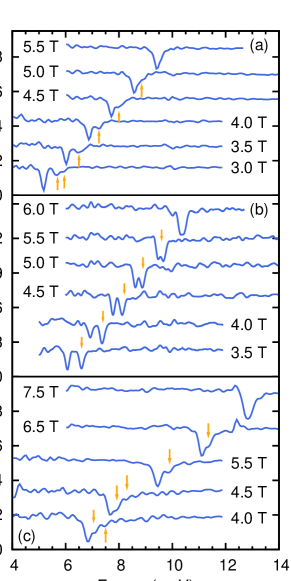
Characteristic results of the magneto-transmission experiment are presented in Fig. 3. Relative magneto-transmission spectra are shown, i.e. for each photon energy, the transmission at a given field normalized to the same at T. A well-defined CR absorption of a nearly Lorentzian shape is obtained for all three samples at higher magnetic fields. When the magnetic field is lowered, we observe a more complex behavior with the CR absorption split into two or even more modes. The energy distance between these modes is clearly different in various samples and it is correlated with the depth of the etched holes, i.e. with the strength of the modulation potential induced by the lateral patterning. An unpatterned reference sample, taken from the wafer used for fabrication of the samples A and B, has been also tested. As expected, it showed a typical Lorentzian-shaped CR absorption at the energy of in the whole available range of magnetic fields.
Since the initial carrier concentration at dark was or could be modified during technological processing and also, since the carrier concentration is affected by the near infrared part of the globar/mercury lamp radiation (due to persistent photoconductivity), we estimated the carrier densities directly from the strength of cyclotron resonance.Chiu et al. (1976) This analysis has been performed at higher fields, when all specimens provide a well-defined CR absorption of Lorentzian shape. The evaluated densities for the sample A, B and C are cm-2 and cm-2, respectively. Optionally, this density could be further increased by illumination by an infrared diode. Using the CR absorption width, we roughly estimated also the carrier mobility in samples after processing which was found to be somewhat in excess of for all three specimens.
IV Interpretation
The observed departure from a single-mode CR at energy shows a clear effect of the lateral modulation and we discuss two possible scenarios to interpret this finding. The first one relies on a quantum-mechanical (single-particle) approach and assumes the AG miniband structure due to the lateral periodic potential. These minibands are transformed into dispersively broadened LLs at non-zero magnetic field. The second scenario, a classical one, recalls characteristic multimode CR absorption observed in systems dominated by (confined) magneto-plasmons. We commence our discussion by showing that this latter scenario is, if considered in detail, inconsistent with our measurements.
Splitting of the cyclotron resonance absorption in diminishing magnetic fields, as shown in Fig. 3, is reminiscent of magneto-plasma oscillations in a 2DEG.Stern (1967) Indeed, the magneto-optical response of our samples, which consists from a basic CR absorption line accompanied by one or more modes at (only) higher energies, resembles spectra taken on a 2DEG with 1D lateral modulation or on a confined unmodulated 2DEG (stripe).Mikhailov and Savostianova (2005, 2006); Fedorych et al. (2009) Let us therefore compare our results to the response of magneto-plasmons in a 2DEG subject to lateral modulation in both directions, in particular in antidot lattices.Kern et al. (1991); Zhao et al. (1992) In such a case, the far infrared or microwave magneto-absorption response includes, among others, a characteristic lower branch located below the CR energy, which is well documented experimentally and explained theoretically.Heitmann and Kotthaus (1993) This lower branch is interpreted as an edge-magneto-plasmon (EMP), circulating around the antidot, and its existence is not directly connected with the symmetry of the antidot lattice.Mikhailov and Volkov (1995); Mikhailov (1996)
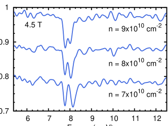
No sign of any EMP mode below CR energy has been observed in our experiments. We take this as a clear argument against interpretation of the observed multi-mode CR response in terms of magneto-plasmons. Another test to exclude magneto-plasmon effects was performed using external illumination by an infrared diode. Upon gradual increase of the carrier density in the sample B (as evidenced by the strength of the CR absorption at high magnetic fields), the distance of observed modes shown in Fig. 4 decreased with . For magnetoplasmonic excitations, an opposite trend is expected.Zhao et al. (1992) We also recall that the experiment of Ref. Kern et al., 1991 concerned deeply etched samples and that magnetoplasmon behavior has been typically detected at significantly higher densities.
We now turn to the discussion of experimental facts with respect to the four criteria to observe massless Dirac fermions in a laterally modulated 2DEG. This provides us with basic estimates on how close or far we are from Dirac-like conditions. These criteria, formulated in Sec. II, are related to the (mini)band electronic structure, carrier density, disorder in the system and also to the chosen experimental technique and conditions. We first discuss criterion (i) for which we need an estimate of the modulation potential amplitude . We show that infrared magneto-spectroscopy is a method suitable for this purpose.
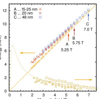
The main absorption features in Fig. 3 occur close to but in contrast to the cyclotron resonance of an unmodulated 2DEG, they have an internal structure which disappears roughly as (see Fig. 5) in the limit of high magnetic fields. Such behavior suggests that the influence of the modulation potential becomes gradually weaker with increasing and potential energy acts as a perturbation to the LLs. Their spacing, the cyclotron energy , then provides the dominant energy scale compared to the modulation potential and the small parameter is . In the first-order perturbation calculation,Wang et al. (2004) the unperturbed energies become broadened into bands:
| (4) |
where , and belongs to the hexagonal first magnetic Brillouin zone. Owing to special properties of Laguerre polynomials Gradshteyn and Ryzhik (1980), optical transition energies, that are , can be rewritten in a simple way. Since we deal with low carrier concentrations at which only the lowest LL is occupied, we can restrain ourselves to ,
| (5) |
where denotes the curled bracket of Eq. (4).
The optical transition energy enters the absorption probability for a photon of frequency that has caused transition between and LLs. Provided that the former (latter) LL is full (empty), this probability is proportional tonote3
| (6) |
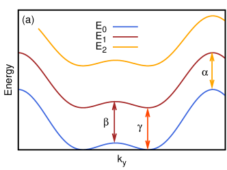
If we neglect the dipole transition matrix element (transition between the mentioned two LLs is allowed by selection rules), the characteristic spectral features correspond to the van Hove singularities indicated in Fig. 6, in the occupation-weighted joint density of states (jDOS):
in which all those transitions at a given energy count where the initial () state is occupied and the final () state is empty, as expressed by the Fermi-Dirac factors . At a filling factor , which was assumed in expression (6), is a band of the width
| (7) |
situated close to . The width of the band decreases with decreasing (at constant ), as the filling of the LL decreases and smaller portions of the magnetic Brillouin zone become available for transitions. In the limit of very large , turns into a zero-width peak at exactly .
| Sample | ||||
|---|---|---|---|---|
| A | 15-25 | 100 | 2.2 meV | 2.4 |
| B | 20 | 100 | 3.5 meV | 3.1 |
| C | 48 | 115 | 4 meV | 3.6 |
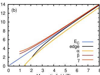
Eq. (7) provides a reasonable basis for interpretation of experimental data presented in Figs. 3(a)-(c). The peak-to-peak distance shown as the lower data sets in Fig. 5 follows the magnetic field dependence of allowing to extract the values of for the particular sample. It should be noted however, that the peak splitting observed in experiments does not correspond to the full width as calculated using Eq. (7) because the lower edge of the absorption band is suppressed for . This is the case of and when spin degeneracy remains unresolved (Zeeman splitting is roughly an order of magnitude smaller than the CR peak width at T; for as appropriate in GaAs systemsYugova:2007_a ). Features of the jDOS appearing in the absorption band scale as , where is a constant. These features are shown in Fig. 6 and correspond to the indicated transitions of the broadened Landau bands . The first states that become depopulated upon the filling factor dropping below two (that is when the magnetic field is increased) are those close to the top of the band. Correspondingly, the transitions are the first ones to disappear from the absorption spectra.
For the remaining two features and , our form of the potential would imply . However, since the transition gives rise to a logarithmic singularity which is likely to be smeared out, we focus on another candidate for an absorption feature: the Fermi edge which is also shown in the lower panel of Fig. 6 (transitions from the states close to to the next Landau band). Although the Fermi edge does not precisely scale with , it appears at frequencies hence we take . The values of inferred from fitting our data, assuming that the splitting of the CR mode corresponds to , are shown in Tab. 1 alongside with the corresponding . We can now return to criterion (i), and see that, as anticipated at the beginning of Sec. III, shallow etching may create modulation potential favorable for Dirac-fermion physics in AG as quantified by the first criterion in Sec. II.
While criterion (i) seems satisfied for our samples, the carrier density is by a factor too large compared to the requirement (ii), even in the most favourable situation (upper Dirac cone, samples A, B). Since further lowering of may induce metal-to-insulator transitionDe Simoni et al. (2010) a better strategy seems to reduce the lattice constant. Further technological improvements will however, then be required to keep criterion (iii) fulfilled. In our case, the measured mobility implies mean free path only few times larger than the lattice constant and the former is likely to deteriorate rapidly upon pushing electron lithography closer to its limits of spatial resolution. Once the criteria (i–iii) are met for some sample, one should proceed to low field () and low temperature () experiments as required by the last criterion (iv). Since inter-LL transitions will then be in sub-THz range and fabrication of samples homogeneous on a scale comparable to the wavelength of absorbed light will be difficult, magnetotransport of photoluminescence experiments seem most promising.
Summary and Conclusions
The concept of artificial graphene has been explored both experimentally and theoretically. Based on a simple theoretical model, we formulated four basic criteria that need to be met in order to create and experimentally demonstrate the proposed graphene-like bands in modulated semiconductor heterostructures. We have prepared three samples with lateral modulation and investigated them using infrared magneto-spectroscopy. The results have been discussed with respect to the proposed criteria with the following conclusions. Etching an antidot (hole) lattice on the sample surface creates lateral modulation potential with favorable strength, which according to our model, should give rise to a miniband structure containing well-developed Dirac cones. An empirical rule, which connects the depth of etched holes with the strength of the lateral potential, has been found for our technological protocol. The quality of prepared specimens, expressed in terms of mobility or mean free path, could be sufficient to resolve the AG electronic structure with the Dirac cones, nevertheless, further increase of this quality would be desirable. The main obstacle, preventing up to now realization of Dirac-like physics in 2DEG, seems to be related to the interplay between the electron density and the lattice constant. Since lowering carrier density down to range seems unrealistic, we instead logically suggest to reduce the lattice constant below 100 nm. This is technologically challenging, given the constraints on mobility, nevertheless still feasible. Furthermore, we propose to focus on a higher Dirac cone, which is found in AG minibad structure and which could be probed at higher carrier densities, namely at for nm. With these suggestions, we believe that massless Dirac fermions can be observed in laterally modulated 2DEG, probably using infrared or THz magneto-spectroscopy or magneto-transport technique, in (possibly not too distant) future.
Acknowledgements
The authors would like to sincerely thank P. Hubík and J. Čermák for technological assistance and J. Wunderlich for valuable critical remarks. Moreover, the support of the following institutions is acknowledged: the Ministry of Education of the Czech Republic projects LC510 and MSM0021620834, GAČR No. P204/10/1020, the Charles University in Prague grants GAUK No. 425111 and SVV-2011-263306, the Academy of Sciences of the Czech Republic via Institutional Research Plan No. AV0Z10100521, GAAV contract KJB100100802, Fondation NanoScience via project Dispograph, Præmium Academiæ, NSF-NEB 2020, SRC, and last but not least, EC-EuroMagNetII under Contract No. 228043.
References
- Novoselov et al. (2005) K. S. Novoselov, A. K. Geim, S. V. Morozov, D. Jiang, M. I. Katsnelson, I. V. Grigorieva, S. V. Dubonos, and A. A. Firsov, Nature 438, 197 (2005).
- Zhang et al. (2005) Y. B. Zhang, Y. W. Tan, H. L. Stormer, and P. Kim, Nature 438, 201 (2005).
- Geim and Novoselov (2007) A. K. Geim and K. S. Novoselov, Nature Mater. 6, 183 (2007).
- Grynberg et al. (1993) G. Grynberg, B. Lounis, P. Verkerk, J.-Y. Courtois, and C. Salomon, Phys. Rev. Lett. 70, 2249 (1993).
- Zhu et al. (2007) S.-L. Zhu, B. Wang, and L.-M. Duan, Phys. Rev. Lett. 98, 260402 (2007).
- Wunsch et al. (2008) B. Wunsch, F. Guinea, and F. Sols, New Journal of Physics 10, 103027 (2008).
- Park et al. (2008) C.-H. Park, L. Yang, Y.-W. Son, M. L. Cohen, and S. G. Louie, Phys. Rev. Lett. 101, 126804 (2008).
- Park and Louie (2009) C.-H. Park and S. G. Louie, Nano Letters 9, 1793 (2009).
- Gibertini et al. (2009) M. Gibertini, A. Singha, V. Pellegrini, M. Polini, G. Vignale, A. Pinczuk, L. N. Pfeiffer, and K. W. West, Phys. Rev. B 79, 241406 (2009).
- Dubois, S. M.-M. et al. (2009) Dubois, S. M.-M., Zanolli, Z., Declerck, X., and Charlier, J.-C., Eur. Phys. J. B 72, 1 (2009).
- Rycerz et al. (2007) A. Rycerz, J. Tworzydło, and C. W. J. Beenakker, Nature Phys. 3, 172 (2007).
- Cheianov et al. (2007) V. V. Cheianov, V. Fal’ko, and B. L. Altshuler, Science 315, 1252 (2007).
- Garcia-Pomar et al. (2008) J. L. Garcia-Pomar, A. Cortijo, and M. Nieto-Vesperinas, Phys. Rev. Lett. 100, 236801 (2008).
- (14) D.M. Eigler and E.K. Schweizer, Nature 344, 524 (1990).
- Kern et al. (1991) K. Kern, D. Heitmann, P. Grambow, Y. H. Zhang, and K. Ploog, Phys. Rev. Lett. 66, 1618 (1991).
- Weiss et al. (1989) D. Weiss, K. V. Klitzing, K. Ploog, and G. Weimann, EPL (Europhysics Letters) 8, 179 (1989).
- Mikhailov (1996) S. A. Mikhailov, Phys. Rev. B 54, R14293 (1996).
- Beenakker (1989) C. W. J. Beenakker, Phys. Rev. Lett. 62, 2020 (1989).
- Středa and MacDonald (1990) P. Středa and A. H. MacDonald, Phys. Rev. B 41, 11892 (1990) .
- (20) V.M. Gvozdikov, Phys. Rev. B 75, 115106 (2007).
- Albrecht et al. (1999) C. Albrecht, J. H. Smet, D. Weiss, K. von Klitzing, R. Hennig, M. Langenbuch, M. Suhrke, U. Rössler, V. Umansky, and H. Schweizer, Phys. Rev. Lett. 83, 2234 (1999).
- Olszewski et al. (2004) S. Olszewski, M. Pietrachowicz, and M. Baszczak, phys. stat. sol. (b) 241, 3572 (2004).
- (23) V.M. Gvozdikov, Phys. Rev. B 76, 235125 (2007).
- Hofstadter (1976) D. R. Hofstadter, Phys. Rev. B 14, 2239 (1976).
- Geisler et al. (2004) M. C. Geisler, J. H. Smet, V. Umansky, K. von Klitzing, B. Naundorf, R. Ketzmerick, and H. Schweizer, Phys. Rev. Lett. 92, 256801 (2004).
- (26) D. Pfannkuche and R.R. Gerhardts, Phys. Rev. B 46, 12606 (1992).
- De Simoni et al. (2010) G. De Simoni, A. Singha, M. Gibertini, B. Karmakar, M. Polini, V. Piazza, L. N. Pfeiffer, K. W. West, F. Beltram, and V. Pellegrini, Appl. Phys. Lett. 97, 132113 (2010).
- Singha et al. (2011) A. Singha, M. Gibertini, B. Karmakar, S. Yuan, M. Polini, G. Vignale, M. I. Katsnelson, A. Pinczuk, L. N. Pfeiffer, K. W. West, and V. Pellegrini, Science 332, 1176 (2011).
- Sadowski et al. (2006) M. L. Sadowski, G. Martinez, M. Potemski, C. Berger, and W. A. de Heer, Phys. Rev. Lett. 97, 266405 (2006).
- Jiang et al. (2007) Z. Jiang, E. A. Henriksen, L. C. Tung, Y.-J. Wang, M. E. Schwartz, M. Y. Han, P. Kim, and H. L. Stormer, Phys. Rev. Lett. 98, 197403 (2007).
- Deacon et al. (2007) R. S. Deacon, K.-C. Chuang, R. J. Nicholas, K. S. Novoselov, and A. K. Geim, Phys. Rev. B 76, 081406 (2007).
- (32) Some previous calculationsPark and Louie (2009); Gibertini et al. (2009) used muffin-tin potential whose parameters are (at minimum) three: antidot distance, size and depth. Realistic form of the potential in an experimental sample is naturally hard to ascertain in detail, hence the advantage of the present model is that it is both generic and simple (single-parametric), allowing to classify types of miniband structures that may arise while not compromising the model validity. The lesson from studies with muffin-tin potential however is that higher harmonics added to do not ruin the Dirac cones by opening gaps, provided such additional terms preserve the honeycomb symmetry. We thank Rafał Oszwałdowski for his comments on this topic.
- (33) Evolution of wavefunctions (modulus square) upon moving on a small circle in momentum space around the K-point was studied. Degenerate-level perturbative resultsPark and Louie (2009) were recovered for both Dirac cones even in the presence of mixing to levels far from the cones.
- Soibel et al. (1996) A. Soibel, U. Meirav, D. Mahalu, and H. Shtrikman, Semiconductor Science and Technology 11, 1756 (1996).
- Hugger et al. (2008) S. Hugger, T. Heinzel, and T. Thurn-Albrecht, Appl. Phys. Lett. 93, 102110 (2008).
- Takahara et al. (1995) J. Takahara, A. Nomura, K. Gamo, S. Takaoka, K. Murase, and H. Ahmed, Jap. J. of Appl. Phys. 34, 4325 (1995).
- Geisler et al. (2005) M. C. Geisler, S. Chowdhury, J. H. Smet, L. Höppel, V. Umansky, R. R. Gerhardts, and K. von Klitzing, Phys. Rev. B 72, 045320 (2005).
- Heitmann and Kotthaus (1993) D. Heitmann and J. P. Kotthaus, Physics Today 46, 56 (1993).
- Chiu et al. (1976) K. Chiu, T. Lee, and J. Quinn, Surface Science 58, 182 (1976).
- (40) Photon absorption in a 2D superlattice is derived for example by V. Demikhovskii and A. Perov: J. Exp. Theor. Phys. 87, 973 (1998), and a more general discussion can be found on p. 241 in G. Bastard: Wave mechanics applied to semiconductor heterostructures, Wiley (1991).
- Wang et al. (2004) X. F. Wang, P. Vasilopoulos, and F. M. Peeters, Phys. Rev. B 69, 035331 (2004).
- Gradshteyn and Ryzhik (1980) I. S. Gradshteyn and I. M. Ryzhik, “Table of integrals, series, and products,” (Academic, New York, 1980).
- Stern (1967) F. Stern, Phys. Rev. Lett. 18, 546 (1967).
- Mikhailov and Savostianova (2005) S. A. Mikhailov and N. A. Savostianova, Phys. Rev. B 71, 035320 (2005).
- Mikhailov and Savostianova (2006) S. A. Mikhailov and N. A. Savostianova, Phys. Rev. B 74, 045325 (2006) .
- Fedorych et al. (2009) O. M. Fedorych, S. A. Studenikin, S. Moreau, M. Potemski, T. Saku, and Y. Hirayama, Int. J. of Mod. Phys. B 23, 2698 (2009).
- Zhao et al. (1992) Y. Zhao, D. C. Tsui, M. Santos, M. Shayegan, R. A. Ghanbari, D. A. Antoniadis, and H. I. Smith, Appl. Phys. Lett. 60, 1510 (1992).
- Mikhailov and Volkov (1995) S. A. Mikhailov and V. A. Volkov, Phys. Rev. B 52, 17260 (1995).
- (49) I. A. Yugova, A. Greilich, D. R. Yakovlev, A. A. Kiselev, M. Bayer, V. V. Petrov, Yu. K. Dolgikh, D. Reuter and A. D. Wieck, Phys. Rev. B 75, 245302 (2007).