Strong mobility degradation in ideal graphene nanoribbons due to phonon scattering
Abstract
We investigate the low-field phonon-limited mobility in armchair graphene nanoribbons (GNRs) using full-band electron and phonon dispersion relations. We show that lateral confinement suppresses the intrinsic mobility of GNRs to values typical of common bulk semiconductors, and very far from the impressive experiments on 2D graphene. Suspended GNRs with a width of 1 nm exhibit a mobility close to 500 cm2/Vs at room temperature, whereas if the same GNRs are deposited on HfO2 mobility is further reduced to about 60 cm2/Vs due to surface phonons. We also show the occurrence of polaron formation, leading to band gap renormalization of 118 meV for 1 nm-wide armchair GNRs.
pacs:
73.63.-b,73.50.Dn,72.80.Vp,63.22.-mUnderstanding the role of phonon scattering Fratini and Guinea (2008); Perebeinos and Avouris (2010); Konar et al. (2010); Fang et al. (2008) is of primary importance, since it provides information regarding the ultimate intrinsic mobility limit () of a material, i.e., when all extrinsic scattering sources have been removed. This is especially important for new materials or nanostructured ones, such as graphene nanoribbons, where experiments are not fully comparable, given the presence of defects and other non idealities. Recent experiments have found in suspended graphene close to 105 cm2/Vs near room temperature Bolotin et al. (2008), but with a sizable degradation after deposition on high-k gate insulators Chen et al. (2008), probably due to coupling to the polar modes of the substrate Fratini and Guinea (2008); Perebeinos and Avouris (2010); Konar et al. (2010).
Very few indications are available on mobility degradation in Graphene NanoRibbons (GNRs) deposited on different gate insulators Liao et al. (2010). As of now, in sub-10 nm GNRs cannot be extracted from experiments since line-edge roughness (LER) is presently limiting mobility in state-of-the-art GNRs Wang et al. (2008); Yang and Murali (2010); Betti et al. (2011). Theory, on the other hand, allows us to individually evaluate the impact of each scattering source on mobility, which is often a prohibitive task in experiments. Phonon-limited scattering is particularly important, since it represents the unavoidable scattering mechanism at finite temperature, and provides a good indication of the potential for the material in electronics, either for devices or interconnects.
Here we investigate the effect of phonons and surface optical (SO) phonons on carrier transport in GNRs by means of a full band (FB) approach based on a tight-binding (TB) description Saito et al. (2003) of the electronic structure and of the phonon spectrum. We compute scattering rates with first-order perturbation theory using the deformation potential approximation (DPA), and low-field mobility using the Kubo-Greenwood formula EPA . We obtain the one-dimensional (1D) subbands of an armchair GNR from a TB -Hamiltonian accounting for energy relaxation at the edges Son et al. (2006). The electron energy dispersion is quantized in the transverse direction with wavevectors , where 0.249 nm is the graphene lattice constant, is the number of dimer lines and index runs from 1 to . Graphene phonon spectrum is obtained with the force constant dynamic-matrix approach, including contributions up to the fourth nearest neighbors (4NNFC approach) Saito et al. (2003) and using force constant parameters extracted from first-principles calculations Wirtz and Rubio (2004). Each of the six phonon branches of graphene, labelled by the quantum number , is splitted into 1D sub-branches, with transverse wave vector { for and for }.
The momentum relaxation rate of an electron in the initial state accounting for scattering from GNR phonons is obtained from the Fermi Golden Rule, summing over all final states , conserving total energy and longitudinal momentum EPA :
| (1) | |||||
where (), if is a longitudinal acoustic (in-plane optical) mode, and eV/m Fang et al. (2008) are the acoustic (AC) and optical (OP) deformation potentials, respectively, , , g/cm2 is graphene mass per unit area Fang et al. (2008), is the Bose-Einstein occupation factor and . In addition, , is the GNR width, is the spinor overlap Rozhkov et al. (2009) and is the Fermi occupation factor. In Eq. (1) the upper sign is for phonon absorption (ABS) and the lower for phonon emission (EM). is the form factor due to the transverse momentum conservation uncertainty EPA ; Betti et al. (2010).
We have investigated the electrostatic coupling between electrons in the GNR channel and remote phonons of the substrate considering the GNR deposited on an oxide layer of thickness , width and placed at a distance nm EPA . The oxide is backgated by an ideal metal. Since phonon modes are almost constant as a function of the longitudinal SO phonon wavevector Konar et al. (2010), we assume the same energies as in Ref. Perebeinos and Avouris (2010) for the two considered SO phonon modes. In addition, electrons are confined in the plane, therefore the electron-SO phonon scattering rate reads EPA :
| (2) | |||||
where represents the 2D SO phonon wavevector, , the sum runs over all SO phonon modes, is the electron-phonon coupling parameter Konar et al. (2010); EPA , is the form factor EPA which reduces to if .
In Eq. (2), is the GNR static dielectric function calculated within the Random Phase Approximation (RPA) in the size quantum limit Fang et al. (2008); EPA . For 10 nm-wide GNRs, screening of the electric field due to polar vibrations is instead modeled by means of the 2D RPA graphene static dielectric function Hwang et al. (2007). From a numerical point of view, in order to reduce numerical noise, we have approximated in Eqs. (1) and (2) with a Gaussian window of standard deviation and, for the lowest AC subbranches, a collisional broadening approach has been implemented considering . Finally, we have computed the low-field mobility by means of the Kubo-Greenwood formula accounting for 1D transport EPA ; Betti et al. (2010).
DPA formally leads to a zero coupling with the transversal acoustic (TA) and flexural (ZA) phonon modes, so that only scattering with longitudinal acoustic (LA) modes is typically considered Fang et al. (2008). Theory Mariani and von Oppen (2008) and Raman spectroscopy Ferrari et al. (2006) have shown that ZA modes are negligible down to 130 K. However, classical results based on a TB description of electron-phonon coupling Pietronero et al. (1980) and recent ab-initio calculations Borysenko et al. (2010) have demonstrated that TA modes play a comparable role as that of LA modes in degrading . On the other hand, a physical description of graphene taking into account long-range interaction between carbon atoms highlights an off-diagonal coupling to the TA modes through the modulation of the hopping parameters, which is smaller than the on-diagonal deformation potential contribution Suzuura and Ando (2002). We choose to adopt a physically consistent approach and use DPA considering electron coupling only with LA, LO and TO modes, rather than euristically reintroduce the contribution of TA modes. We use eV, extracted from DFT calculation for the GNR family Long et al. (2009), rather than fitting experiments which are affected by uncontrolled mechanisms and actually lead to a large spread of the considered values for Fang et al. (2008); Bolotin et al. (2008); Borysenko et al. (2010).
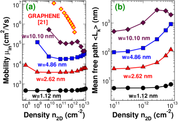
Low-field mobility is shown in Fig. 1a as a function of the electron density for different widths. close to 500 cm2/Vs is found for 1 nm-wide GNR, exceeding by almost one order of magnitude the experimental mobility of GNRs Wang et al. (2008); Yang and Murali (2010) and the intrinsic phonon-limited mobility of silicon nanowires Jin et al. (2007) of comparable size. We find that is mainly limited by backward scattering involving AC phonons, due to the large mode-dependent OP energy offset ( 130-160 meV) Betti et al. (2010). Unlike in 2D graphene, where Perebeinos and Avouris (2010), the lateral confinement in GNRs leads to a non-monotonic -dependence as also observed in CNTs Perebeinos et al. (2006) (Fig. 1a). For small , increases with , due to the reduction of final states available for scattering. For wider GNRs biased in the inversion regime, electrons can populate excited subbands opening additional channels for scattering, thus reducing .
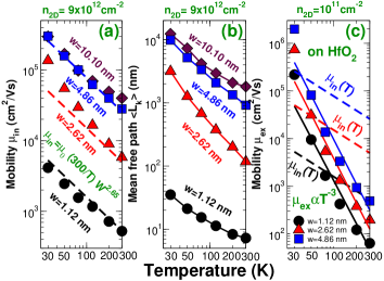
In Fig. 2a, is plotted as a function of temperature . Similarly to what has been observed in small-diameter CNTs Perebeinos et al. (2005), in narrow GNRs the dependence on and can be expressed by means of the empirical relation where 391 cm2/Vs and , which is close to expected for narrow GNRs, since and and the density of states . Of course, for large saturates to that of 2D graphene. Since AC in-plane phonons scattering is dominant and for , is inversely proportional to (Fig. 2a). The mean free path in the first subband is shown in Fig. 1b as a function of and in Fig. 2b as a function of , where , is the group velocity and the expectation value has been computed in the Brillouin zone, considering as the distribution function Betti et al. (2010). At K, is of the order of few m for larger GNRs, as expected in graphene flakes, while it is 10 nm for narrower GNRs (Figs. 2b). In addition, , as (Figs. 2b).
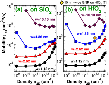
The SO phonon-limited mobility as a function of is shown in Figs. 3a-b for smaller than 10 nm, considering GNRs deposited both on SiO2 and on HfO2. As in graphene Konar et al. (2010); Perebeinos and Avouris (2010), the higher the dielectric constant, the larger the mobility suppression due to SO phonon scattering. In particular, we observe down to 700 cm2/Vs for SiO2 (Fig. 3a) and 60 cm2/Vs for HfO2 (Fig. 3b), due to the smaller energy offset of the emission processes. As in CNTs Perebeinos et al. (2009), with ( 1.4-1.6) dependent on and smaller than . For smaller than 5 nm increases with electron concentration due to the impact of screening, whereas for 10.10 nm for higher concentrations the increase of available modes for scattering reduces mobility.
Comparing Figs. 3a-b with Fig. 1a, it can be observed that SO phonons play a secondary role for very narrow GNRs on SiO2 but they become predominant with increasing 2.5 nm roughly for 1012 cm-2, whereas they are predominant for all densities in GNRs on HfO2. Comparison with experiments shows that is larger by up to one order of magnitude than mobility measured on GNRs deposited on SiO2 Wang et al. (2008) and by a factor three than mobility measured on 10-nm-wide GNRs integrated with ultrathin HfO2 dielectric Liao et al. (2010). This gives a rough estimation of the increase in mobility that could be achieved through fabrication technology improvements capable to suppress the present dominant scattering mechanisms (e.g. LER). As can be noted in Fig. 2c and as it also occurs in CNTs deposited on polar dielectrics Perebeinos et al. (2009), . In particular, for HfO2 . Since , SO phonon scattering dominates transport roughly above 100 K for all (Fig. 2c), as for CNTs on SiO2 Perebeinos et al. (2009).
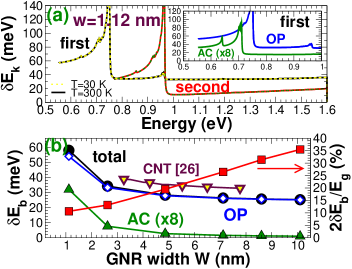
Finally, we focus on the polaronic energy shift due to the electron-phonon coupling, computed exploiting the second-order perturbation theory EPA . Fig. 4a shows as a function of for the lowest two subbands for the nm case. is weakly energy dependent near the cutoff subband, is independent of and increases sharply in correspondence of intersubband transitions. As in CNTs Perebeinos et al. (2005), mostly OP phonons contribute to (inset of Fig. 4a). Instead, unlike in CNTs Perebeinos et al. (2005), the contribution to from AC phonons exhibits few peaks due to the transverse momentum conservation uncertainty (inset of Fig. 4a). The polaronic binding energy, i.e. the polaronic energy shift referred to the first conduction subband edge , is and is almost 59 meV for 1 nm-wide GNRs, close to that obtained for semiconducting CNTs with the same number Perebeinos et al. (2005) (Fig. 4b) and corresponds to a band gap renormalization 118 meV for 1-nm nanoribbons, and to a relative correction of -35% of the energy gap of 10-nm nanoribbons (Fig. 4b).
In conclusion, we have proposed a very accurate full-band approach to evaluate low-field phonon-limited mobility in GNRs. We find that is close to 500 cm2/Vs in suspended 1 nm-wide GNRs at room temperature, and is suppressed down to 60 cm2/Vs in 1-nm wide GNR deposited on HfO2, due to coupling with SO phonons. The result is important from the point of view of methodology and of fundamental physics, since the corresponding mean free paths range from 1 to 10 nm, undermining the possibility of performing ballistic or coherent transport experiments at non-cryogenic temperatures. It is also important from the application point of view: whereas suspended 2D graphene has an intrinsic mobility at room temperature several orders of magnitude larger than that of bulk semiconductors, narrow GNRs with reasonable semiconducting gap have only slightly larger mobility than comparable silicon nanowires. Finally, we also find polaron formation in armchair GNRs, with a remarkable band gap renormalization of up to 35% in the case of 10 nm-wide ribbons.
This work was supported in part by the EC 7FP through NANOSIL (n. 216171), GRAND (n. 215752) grants, and by the MIUR-PRIN project GRANFET (Prot. 2008S2CLJ9). Authors thank www.nanohub.org for the provided computational resources.
References
- Fratini and Guinea (2008) S. Fratini and F. Guinea, Phys. Rev. B 77, 195415 (2008).
- Perebeinos and Avouris (2010) V. Perebeinos and P. Avouris, Phys. Rev. B 81, 195442 (2010).
- Konar et al. (2010) A. Konar, T. Fang, and D. Jena, Phys. Rev. B 82, 115452 (2010).
- Fang et al. (2008) T. Fang, A. Konar, H. Xing, and D. Jena, Phys. Rev. B 78, 205403 (2008).
- Bolotin et al. (2008) K. I. Bolotin, K. J. Sikes, J. Hone, H. L. Stormer, and P. Kim, Phys. Rev. Lett. 101, 096802 (2008).
- Chen et al. (2008) J.-H. Chen, C. Jang, S. Xiao, M. Ishigami, and M. S. Fuhrer, Nature Nanotechnology 3, 206 (2008).
- Liao et al. (2010) L. Liao, J. Bai, R. Cheng, Y.-C. Lin, S. Jiang, Y. Huang, and X. Duan, Nano Lett. 10, 1917 (2010).
- Wang et al. (2008) X. Wang, Y. Ouyang, X. Li, H. Wang, J. Guo, and H. Dai, Phys. Rev. Lett. 100, 206803 (2008).
- Yang and Murali (2010) Y. Yang and R. Murali, IEEE Elec. Dev. Lett. 31, 237 (2010).
- Betti et al. (2011) A. Betti, G. Fiori, and G. Iannaccone, to be published in IEEE Trans. Electron Devices (2011).
- Saito et al. (2003) R. Saito, G. Dresselhaus, and M. Dresselhaus, Imperial College Press, London (2003).
- (12) See EPAPS supplementary material at [] for the expressions of , and .
- Son et al. (2006) Y. W. Son, M. L. Cohen, and S. Louie, Phys. Rev. Lett. 97, 216803 (2006).
- Wirtz and Rubio (2004) L. Wirtz and A. Rubio, Solid State Comm. 131, 141 (2004).
- Rozhkov et al. (2009) A. V. Rozhkov, S. Savel’ev, and F. Nori, Phys. Rev. B 79, 125420 (2009).
- Betti et al. (2010) A. Betti, G. Fiori, and G. Iannaccone, IEDM Tech. Digest pp. 728–731 (2010).
- Hwang et al. (2007) E. H. Hwang, S. Adam, and S. D. Sarma, Phys. Rev. Lett. 98, 186806 (2007).
- Mariani and von Oppen (2008) E. Mariani and F. von Oppen, Phys. Rev. Lett. 100, 076801 (2008).
- Ferrari et al. (2006) A. C. Ferrari, J. C. Meyer, V. Scardaci, C. Casiraghi, M. Lazzeri, F. Mauri, S. Piscanec, D. Jiang, K. S. Novoselov, S. Roth, et al., Phys. Rev. Lett. 97, 187401 (2006).
- Pietronero et al. (1980) L. Pietronero, S. Strässler, and H. R. Zeller, Phys. Rev. B 22, 904 (1980).
- Borysenko et al. (2010) K. M. Borysenko, J. T. Mullen, E. A. Barry, S. Paul, Y. G. Semenov, J. M. Zavada, M. B. Nardelli, and K. W. Kim, Phys. Rev. B 81, 121412 (2010).
- Suzuura and Ando (2002) H. Suzuura and T. Ando, Phys. Rev. B 65, 235412 (2002).
- Long et al. (2009) M.-Q. Long, L. Tang, D. Wang, L. Wang, and Z. Shuai, JACS 131, 17728 (2009).
- Jin et al. (2007) S. Jin, M. V. Fischetti, and T. Tang, J. Appl. Phys. 102, 083715 (2007).
- Perebeinos et al. (2006) V. Perebeinos, J. Tersoff, and P. Avouris, Nano Lett. 6, 205 (2006).
- Perebeinos et al. (2005) V. Perebeinos, J. Tersoff, and P. Avouris, Phys. Rev. Lett. 94, 086802 (2005).
- Perebeinos et al. (2009) V. Perebeinos, S. V. Rotkin, A. G. Petrov, and P. Avouris, Nano Lett. 9, 312 (2009).


