Atomistic investigation of low-field mobility in graphene nanoribbons
Abstract
We have investigated the main scattering mechanisms affecting mobility in graphene nanoribbons using detailed atomistic simulations. We have considered carrier scattering due to acoustic and optical phonons, edge roughness, single defects, and ionized impurities, and we have defined a methodology based on simulations of statistically meaningful ensembles of nanoribbon segments. Edge disorder heavily affects mobility at room temperature in narrower nanoribbons, whereas charged impurities and phonons are hardly the limiting factors. Results are favorably compared to the few experiments available in the literature.
Keywords - Low-field mobility, graphene nanoribbons, scattering, edge roughness, defects, impurities, phonons.
I Introduction
Two-dimensional (2D) graphene sheets have demonstrated really attractive electrical properties like high carrier mobility [1, 2] and large coherence length [3]. However, experimental data of mobility available in the literature show huge dispersion, ranging from 102 to 104 cm2/Vs at room temperature, signaling that the fabrication process is still poorly optimized and not fully repeatable. To guide process optimization, an exhaustive interpretation of physical mechanisms limiting mobility would be extremely useful. For Graphene NanoRibbons (GNRs) a comprehensive experimental characterization of mobility is still lacking, mainly due to the difficulty in patterning in a repeatable way very narrow ribbons. Few recent interesting experiments are reported in [4] and [5]. GNRs may also suffer significant degradation of mobility due to additional scattering mechanims, such as edge roughness.
The single most important aspect that makes graphene interesting for nanoscale electronics is its very high mobility. It is therefore of paramount importance to understand if also nano structured graphene can preserve the high mobility (often) measured in graphene sheets, much larger than that of conventional semiconductors. In addition, one would need to understand the effect on mobility of different options for graphene functionalization, which could be required to open a semiconducting gap in graphene.
In the current situation, theoretical investigations [6, 7] and numerical simulations [8, 9, 10] can represent a useful tool to assess the relative impact of different sources of non-idealities on mobility and consequently on device performance, to provide guidelines for the fabrication process and a realistic evaluation of the perspectives of graphene in nanoelectronics.
An analytical method and a Monte Carlo approach have for example been adopted in order to study line-edge roughness (LER) and phonon scattering-limited mobility in Ref. [6] and Ref. [7], respectively. However, due to the reduced width of the considered devices, effects at the atomistic scale are relevant, therefore accurate simulation approaches like semi-empirical tight-binding are needed.
In this work we present atomistic simulations of GNR-FETs, considering GNR widths ranging from 1 to 10 nm, and including scattering due to LER, single defects, ionized impurities, acoustic and optical phonons. A direct comparison with recently fabricated devices [4] will also be performed. Statistical simulations performed on a large ensemble of nanoribbons with different occurrences of the spatial distribution of non-idealities show that phonons, LER and defects scattering can likely explain the few available experimental data [4], where mobility is down to the level of mundane semiconductors (order of - cmVs).
II Methodology
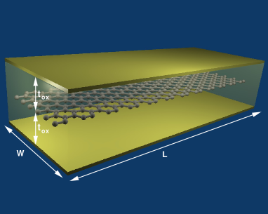
A long GNR-FET channel, where mobility is properly defined, is given by a series of GNR segments of length like those we have considered in the simulation (Fig. 1). For the -th GNR segment, the resistance is the sum of two contributions, the channel resistance and the contact (ballistic) resistance (), where is the drain-to-source voltage, whereas and are the total current and the ballistic current in the -th segment, respectively. Assuming phase coherence is lost at the interface between segments, the resistance of the long channel GNR is therefore the sum of channel resistances and one contact resistance, i.e.:
| (1) |
where is the mean resistance evaluated on the ensemble of nanoribbon segments. Therefore, the mobility of a long channel would read:
| (2) |
where the index denotes each type of scattering mechanism limiting mobility (defects, edge-roughness or impurities), is the total GNR length, is the total charge in the channel and is the mean mobile charge in a segment.

For large values of , one can discard 1 with respect to in Eq. (2) so that we obtain the formula we use in the paper [11]:
| (3) |
The root mean square error of mobility has been computed by means of a Taylor expansion up to the first order of Eq. (3) with respect to statistical fluctuations of the resistance :
| (4) |
and therefore
| (5) |
where and
| (6) |
is the variance of .
Statistical simulations of resistance on a large ensemble of nanoribbon segments with different actual distribution of non-idealities have been performed. In particular, the mobility has been computed in the linear transport regime, for large gate voltages () and small drain-to-source bias 10 mV. Mobility has been extracted by means of Eq. (3) considering an ensemble of nanoribbon segments with different disorder realizations for 1.12 nm-wide GNRs. Due to the computational cost, at least 40 nanoribbons segments have been instead simulated for 10.10 nm-wide GNRs.
Statistical simulations of random actual distributions of defects, LER and ionized impurities have been computed through the self-consistent solution of 3D Poisson and Schrödinger equations within the NEGF formalism, with a tight-binding Hamiltonian [10], extensively exploiting our open-source simulator NanoTCAD ViDES [12]. In particular, we have imposed at both ends of the segments null Neumann boundary conditions on the potential, and open boundary conditions for the transport equation.
In order to compute the LER-limited mobility , statistical simulations have been performed considering a given fraction of single vacancy defects at the edges. is defined as the probability for each carbon atom at the edges to be vacant. In practice, each sample of nanoribbon with edge disorder is randomly generated assuming that each carbon site at the edges has a probability to be replaced by a vacancy. Null hopping parameter has been imposed in correspondence of a defect at the edge.
Defects have been modeled using the on-site energy and the hopping parameter extracted from DFT calculations [13]. In particular, for a fixed defect concentration , each sample of defected nanoribbon with defects is randomly generated assuming that each carbon atom has a probability to be replaced by a vacancy.
As previously assumed in ab-initio calculations [14], we have considered a surface impurity distribution of positive charges equal to +0.4 placed at a distance of 0.2 nm from the GNR surface, where is the elementary charge. Again, if is the impurity fraction, a sample with surface impurities is randomly generated by assuming that each carbon atom has a probability to be at 0.2 nm from an impurity in the dielectric layer.
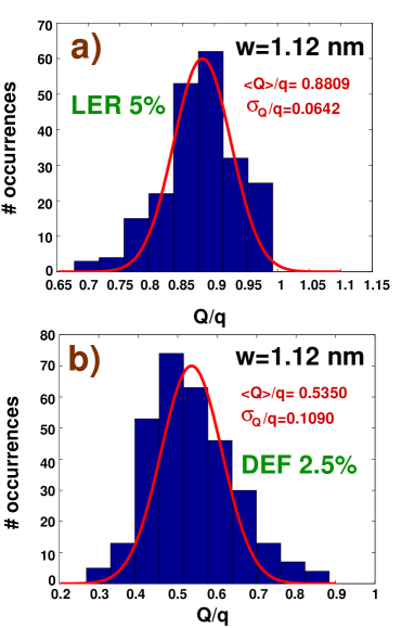
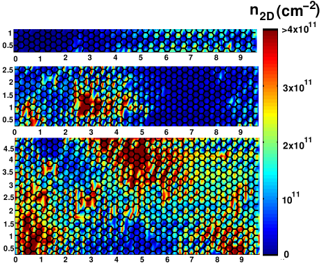
In Figs. 2a-b, we show the distributions of when considering line-edge roughness ( 5%) and defects ( 2.5%) for 1.12 nm. In each picture we show the mean value and the standard deviation of the random variable . For comparison, the corresponding normal distribution is shown.
Phonon-limited mobility (both acoustic and optical) has been computed by means of a semi-analytical model as in [6], but extending the Kubo-Greenwood formalism beyond the effective mass approximation and accounting for energy relaxation at GNR edges [15]. Starting from the Boltzmann transport equation, the phonon limited mobility for a 1D conductor can be espressed as [16] :
| (7) |
where is the electron velocity in the longitudinal direction for the -th electron subband and is the corresponding momentum relaxation time for electron-phonon scattering. In Eq. (7), denotes the expectation value averaged on the Fermi factor as:
| (8) |
where is the one dimensional (1D) carrier density. In order to compute Eq. (7), the following electron dispersion curve has been exploited for the -th subband [15]:
| (9) |
where is the cut-off energy of the -th subband when the electrostatic channel potential is different from zero ( for 0 V). According to Ref. [15], the effective electron mass on the -th subband reads:
| (10) |
where is the graphene hopping parameter (-2.7 eV) and , where is the number of dimer lines of the GNR. For the first conduction subband , where is the energy gap and (which runs from 1 to ) is the index for which is closest to -1/2.
The corresponding Density of States (DOS), accounting for energy relaxation at outermost layers of the GNR [15], reads:
| (11) |
By means of Eqs. (9) and (11), the phonon-limited mobility of a 1D conductor (Eq. (7)) can be expressed as a sum over all contributing subbands [17]:
| (12) | |||||
where is the total 2D electron density, the GNR width and is the temperature.
For what concerns longitudinal phonons, scattering rates are evaluated as in Ref. [6]. According to Ref. [6], only intrasubband scattering has been considered. In particular, the longitudinal optical (LO) phonon scattering rate reads as
| (13) | |||||
where is the Bose-Einstein occupation factor and , is the optical phonon energy, is the optical deformation potential and g/cm2 is the 2D density of graphene. The factor arises from the spinor nature of the graphene eigenfunctions and , where . Here () indicates the initial (final) longitudinal electron wavevector referred to the Dirac point, whereas and (which is equal to for intrasubband scattering) are the quantized initial and final transverse wavevectors, respectively, where is the graphene lattice constant, is the number of dimer lines and . The intravalley longitudinal acoustic (LA) phonon scattering rate can be expressed as
where , is the deformation potential for acoustic phonons, m/s is the sound velocity in graphene and is the module of the phonon wavevector under the backscattering condition.
For both acoustic and optical phonons, we have considered the four lowest subbands. The electron momentum relaxation time is computed by adding the relaxation rate due to electron scattering with acoustic and optical phonons [17]. As a final remark, the effective mobility including all type of scattering sources has been extracted by means of Mathiessen’s rule , where and are the defect and impurity limited mobilities, respectively. We have verified the validity of Mathiessen’s rule considering samples with more sources of non-idealities (i.e. LER, ionized impurities and defects) at the same time. Then we have compared the computed mobility with that obtained by adding single contributions with Mathiessen’s rule, observing a relative error smaller than 3%, which lies within the statistical error.
III Results and Discussions
The simulated segment is a double-gate GNR, embedded in SiO2 with an oxide thickness of 2 nm, 10 nm-long (Fig. 3). The segment length has been chosen to satisfy the assumption of loss of phase coherence at the segment ends. Indeed, according to recent experiments [18], the phase coherence length is close to 11 nm in graphene. From a computational point of view, different widths have been considered, ranging from 1 to 10 nm: 1.12 nm, 2.62 nm, 4.86 nm and 10.10 nm. All simulations have been performed at room temperature K.
III-A Line-edge roughness limited mobility
LER-limited mobility as a function of for different edge-defect concentrations is shown in Fig. 4a in the above-threshold regime, for a 2D carrier density of cm-2. As in all figures in the paper, the error bars represent the estimated root mean squared error of the average of the statistical sample (5).
As predicted by the analytical model in Ref. [6], scales as . Such behavior holds for large (20%) and narrow GNRs ( 5 nm), when scattering from edge defects is expected to be heavier, while, for wider GNRs and for smaller , such a law is not obeyed. In particular, for GNR width larger than 5 nm, tends to saturate, since the increasing number of subbands contributing to transport counterbalance the number of final states available for scattering, enhancing scattering rates. As shown in Fig. 4b, in narrower GNRs, the higher the electron density, the larger the effective mobility, because of stronger screening. decreases for high and wider GNRs, due to mode-mixing, as already observed in Silicon Nanowire FETs [19]. Indeed, for wider GNRs biased in the inversion regime, more transverse modes are able to propagate in the channel due to the reduced energy separation between different subbands. This leads edge defects to become a source of intermode scattering, thus reducing .
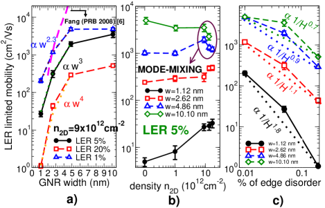
Fig. 4c shows as a function of , where for wide GNRs, consistent with the Drude model, and also observed in graphene in the presence of defects [20]. However, as soon as decreases, quantum localization becomes relevant [21], and the Anderson insulator-like behavior [9] is recovered (), in agreement with analytical predictions [6].
III-B Defect-limited mobility
Defect-limited mobility is plotted in Fig. 5a as a function of for different defect concentrations. Even in this case, localization affects mobility in narrower ribbons, especially for higher (2.5%).
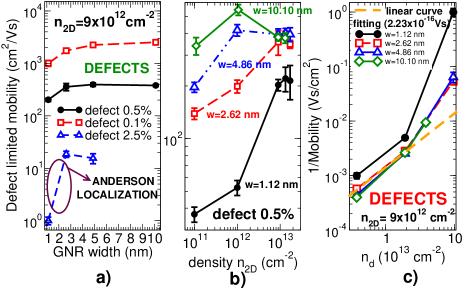
For a fixed defect density, mobility slightly increases with electron density, due to the larger screening (Fig. 5b) and, for larger GNRs biased in the inversion regime, it saturates with increasing , for the same reason discussed above for LER scattering. In Fig. 5c, is plotted as a function of . The wider the ribbons the closer mobility follows the simple Drude model (), as expected for strong disorder and uncorrelated scatterers in 2D graphene sheets [22]. For 10.10 nm atomistic simulations are in agreement with experimental results: a linear curve fitting () leads to a proportionality factor of Vs, similar to those extracted in the case of Ne+ and He+ irradiated graphene samples ( Vs and Vs, respectively) [20].
III-C Ionized impurities limited mobility
Impurity-limited mobility , as a function of , is shown in Fig. 7a for cm-2, and for different impurity charge concentrations. As can be noted, even a high impurity concentration of 1012 cm-2 yields large mobility for 0.4 impurity charge. However, no indications are present in literature regarding the amount of unintentional doping charge [23, 24]. Therefore, in order to check also the effect of impurity ionization on the electron transport, statistical simulations have been performed by increasing the impurity charge up to +2. Mobility as a function of the impurity charge is plotted in Fig. 7b for different and for cm-2. In this case smaller values of (1700 cm2/Vs) are obtained for very narrow GNRs, due to the strongly nonlinear impact on screening in the channel. Even in this case localization strongly degrades mobility for narrower ribbons.
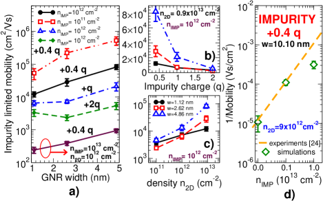
To further test the importance of unintentional doping in limiting mobility, we have considered excess charge densities up to 1013 cm2, which have been encountered in experiments [23]. As shown in Fig. 7a, in this case mobility decreases down to 102 cm2/Vs for narrower GNRs. In Fig. 7c impurity-limited mobility is plotted as a function of for cm-2 and impurity charge and for different . According to [25, 26], in graphene does not depend on the electron density. The behavior is different in GNRs because up to an electron density of 1012 cm-2, only the ground state is occupied, so that the Size Quantum Limit approximation is verified [27, 6]. Since the scattering rate [25] and the static dielectric function increases with [27], the screening becomes stronger with increasing . As a consequence, in GNRs has the increasing monotonic behavior shown in Fig. 7c. In Fig. 7d, we compare experimental results available in literature [24] for graphene, showing the inverse of the impurity-limited mobility as a function of for 10.10 nm and by considering an impurity charge of +0.4: as expected for uncorrelated scatterers, and, as can be seen, experiments and simulations show quite good agreement.
III-D Acoustic and optical phonon-limited mobility
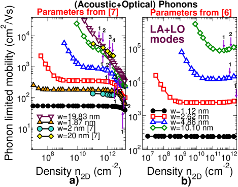
Our study has also been directed towards the investigation of the impact of phonon scattering, through the Kubo-Greenwood formalism [28, 29]. A wide range of phonon parameter values is currently present in the literature [1, 30, 6, 26] (i.e. acoustic () and optical () deformation potentials, as well as optical phonon energy ). We observe that the most widely used phonon parameters are those adopted in Refs. [6, 1, 31], i.e. 16 eV, 160 meV and eV/cm, where is the zone-boundary LO phonon energy. Such values have been tested towards those provided in Refs. [7, 32, 33], showing good agreement as far as mobility is concerned.
To prove the validity of our approach, we have first compared our results with those obtained by means of an accurate 2D Monte Carlo simulator [7]. For a fair comparison, the same phonon parameters and the same scattering rates as in [7] have been used. As can be seen in Fig. 8a, results are in good agreement, especially for wider GNRs. However, such parameters correspond to the out-of plane mode ZO which, according to symmetry-based considerations [34], density functional study [35] and Raman spectroscopy [36], is much weaker than in-plane vibrations.
Therefore, in the following, we adopt the parameters discussed above for LA and LO phonons and the scattering rates described in Eqs. (13) and (II). In Fig. 8b acoustic and optical phonon limited mobility is shown as a function of . As expected, emission scattering rates are found to be larger than absorption scattering rates, due to their higher Bose-Einstein occupation numbers. In addition, as also observed in graphene [37], we have verified that the contribution of optical phonons is negligible also in GNRs, and is dominated by (intravalley) acoustic phonon scattering [6, 7] (Fig. 8b). Note also that, unlike in grafene where [38], in GNRs the transverse confinement leads to a non-monotonic -dependence as in CNTs [39]. As can be seen, slightly increases due to the reduced number of available states for scattering.
We observe that several recent studies [38, 40, 41]
have demonstrated that
surface phonons of the substrate represent a severe source of scattering,
which strongly limits transport in graphene. However, we expect this
effect to be much larger in high- dielectrics like HfO2, rather than in
SiO2, which is the insulator considered in this work.
This issue will be the topic of a more comprehensive work on
electron-phonon scattering in GNRs, which is beyond the scope of the present paper.
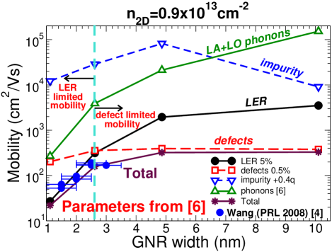
Finally, we compare
the total mobility with experiments from Wang
et al [4] (Fig. 9). In particular, we show the
mobility limited by different scattering mechanisms as well as
the total mobility computed by means of Mathiessen’s rule.
As can be seen, when using parameters in Ref. [6], LER is the
most limiting mechanism ( 5%) for very narrower GNRs, while for wider
GNRs defect scattering is predominant, if a 0.5% is considered.
As an additional remark, we have checked that the same conclusion holds even if we consider
much lower deformation potentials for phonons, that decrease the impact of phonon scattering, such as those
those provided in Ref. [30].
IV Conclusion
We have defined a simulation methodology based on atomistic simulations on statistically significant ensembles of GNR segments to understand the functional dependence of GNR mobility upon different factors, and to quantitatively assess the importance of different scattering mechanisms.
We used such methodology to investigate mobility in GNRs of width ranging from 1 to 10 nm. First, we find that, unlike in 2D graphene, electron-impurity scattering in GNRs is far too weak to affect low-field mobility. In addition, using well established parameters for electron-phonon coupling, we find that phonon scattering is hardly the limiting factor of GNR mobility. For narrower GNRs, line-edge roughness is the main scattering mechanism. This result is consistent with the findings in [5], where wider nanoribbons with very rough edges are characterized. Finally, for a fixed defect density or LER, mobility tends to decrease with the GNR width for narrower devices, suggesting the occurrence of localization effects.
V Acknowledgment
Authors thank M. Lemme, P. Palestri, P. Michetti and T. Fang for useful discussions, and CINECA Super-Computing Center, Bologna, and www.nanohub.org for the provided computational resources. This work was supported in part by the EC 7FP through the Network of Excellence NANOSIL (Contract 216171), and the GRAND project (Contract 215752), by MIUR through the PRIN GRANFET project (Prot. 200852CLJ9), by the ESF EUROCORES Programme FoNE, through funding from the CNR (awarded to IEEIIT-PISA) and the EC 6FP, under Project Dewint (Contract ERASCT-2003-980409).
References
- [1] J.-H. Chen, C. Jang, S. Xiao, M. Ishigami, and M. S. Fuhrer. Intrinsic and extrinsic performance limits of graphene devices on sio2. Nature Nanotechnology, vol. 3, pp. 206–209, 2008.
- [2] X. Li, X. Wang, L. Zhang, S. Lee, and H. Dai. Chemically derived, ultrasmooth graphene nanoribbon semiconductors. Science, vol. 319, pp. 1229–1231, 2008.
- [3] Z. Chen and J. Appenzeller. Mobility Extraction and Quantum Capacitance Impact in High Performance Graphene Field-effect Transistor Devices. IEDM Tech. Digest, pages 509–512, 2008.
- [4] X. Wang, Y. Ouyang, X. Li, H. Wang, J. Guo, and H. Dai. Room-temperature all-semiconducting sub-10 nm graphene nanoribbon field-effect transistors. Phys. Rev. Lett., vol. 100, pp. 206803, 2008.
- [5] Y. Yang and R. Murali. Impact of Size Effect on Graphene Nanoribbon Transport. IEEE Elec. Dev. Lett., vol. 31, pp. 237–239, 2010.
- [6] T. Fang, A. Konar, H. Xing, and D. Jena. Mobility in semiconducting graphene nanoribbons: Phonon, impurity, and edge roughness scattering. Phys. Rev. B, vol. 78, pp. 205403, 2008.
- [7] M. Bresciani, P. Palestri, and D. Esseni. Simple end efficient modeling of the E-k relationship and low-field mobility in Graphene Nano-Ribbons. Solid-State Electronics, vol. 54, pp. 1015–1021, 2010.
- [8] D. A. Areshkin, D. Gunlycke, and C. T. White. Ballistic Transport in Graphene Nanostrips in the Presence of Disorder: Importance of Edge Effects. Nano Lett., vol. 7, pp. 204–210, 2007.
- [9] D. Querlioz, Y. Apertet, A. Valentin, K. Huet, A. Bournel, S. Galdin-Retailleau, and P. Dollfus. Suppression of the orientation effects on bandgap in graphene nanoribbons in the presence of edge disorder. Appl. Phys. Lett., vol. 92, pp. 042108, 2008.
- [10] A. Betti, G. Fiori, G. Iannaccone, and Y. Mao. Physical insights on graphene nanoribbon mobility through atomistic simulations. IEDM Tech. Digest, pages 897–900, 2009.
- [11] G. Iannaccone and M. Pala. An extended concept of mobility for non diffusive conductors, unpublished.
- [12] Code and Documentation can be found at the url: http://www.nanohub.org/tools/vides.
- [13] I. Deretsiz, G. Forte, A. Grassi, A. La Magna, G. Piccitto, and R. Pucci. A multiscale study of electronic structure and quantum transport in -based graphene quantum dots. J. Phys.: Condens. Matter, vol. 22, pp. 095504, 2010.
- [14] K. Rytkönen, J. Akola, and M. Manninen. Density functional study of alkali metal atoms and monolayers on graphite (0001). Phys. Rev. B, vol. 75, pp. 075401, 2007.
- [15] P. Michetti and G. Iannaccone. Analytical Model of One-Dimensional Carbon-Based Schottky-Barrier Transistors. IEEE Trans. Electron Devices, vol. 57, pp. 1616–1625, 2010.
- [16] M. Fischetti. ECE609 Physics of Semiconductor Devices (Spring 2010). http://www.ecs.umass.edu/ece/ece609, Part 1, pp. 80, 2010.
- [17] R. Kotlyar, B. Obradovic, P. Matagne, M. Stettler, and M. D. Giles. Assessment of room-temperature phonon-limited mobility in gated silicon nanowires. Appl. Phys. Lett., vol. 84, pp. 5270, 2004.
- [18] C. Casiraghi, A. Hartschuh, H. Qian, S. Piscanec, C. Georgi, A. Fasoli, K. S. Novoselov, D. M. Basko, and A. C. Ferrari. Raman Spectroscopy of Graphene Edges. Nano Lett., vol. 9, pp. 1433–1441, 2009.
- [19] S. Poli, M. G. Pala, T. Poiroux, S. Deleonibus, and G. Baccarani. Size Dependence of Surface-Roughness-Limited Mobility in Silicon-Nanowire FETs. IEEE Trans. Electron Devices, vol. 55, pp. 2968–2976, 2008.
- [20] J.-H. Chen, W. G. Cullen, C. Jang, M. S. Fuhrer, and E. D. Williams. Defect Scattering in Graphene. Phys. Rev. Lett., vol. 102, pp. 236805, 2009.
- [21] M. Evaldsson, I. V. Zozoulenko, H. XU, and T. Heinzel. Edge-disorder-induced anderson localization and conduction gap in graphene nanoribbons. Phys. Rev. B, vol. 78, pp. 161407, 2008.
- [22] T. Stauber, N. M. R. Peres, and F. Guinea. Electronic transport in graphene: A semiclassical approach including midgap states. Phys. Rev. B, vol. 76, pp. 205423, 2007.
- [23] C. Casiraghi, S. Pisana, K. S. Novoselov, A. K. Geim, and A. C. Ferrari. Raman fingerprint of charged impurities in graphene. Appl. Phys. Lett., vol. 91, pp. 233108, 2007.
- [24] J.-H. Chen, C. Jang, S. Adam, M. S. Fuhrer, E. D. Williams, and M. Ishigami. Charged-impurity scattering in graphene. Nature Physics, vol. 4, pp. 377–381, 2008.
- [25] E. H. Hwang, S. Adam, and S. Das Sarma. Carrier Transport in Two-Dimensional Graphene Layers. Phys. Rev. Lett., vol. 98, pp. 186806, 2007.
- [26] K. I. Bolotin et al. Temperature-Dependent Transport in Suspended Graphene. Phys. Rev. Lett., vol. 101, pp. 096802, 2008.
- [27] J. Lee and H. Spector. Dielectric response function for a quasi-one-dimensional semiconducting system. J. Appl. Phys., vol. 57, pp. 366–372, 1985.
- [28] R. Kubo. Statistical-Mechanical Theory of Irreversible Processes. J. Phys. Soc. Jpn., vol. 12, pp. 570, 1957.
- [29] D. A. Greenwood. The Boltzmann Equation in the Theory of Electrical Conduction in Metals. Proc. Phys. Soc. London, vol. 71, pp. 585, 1958.
- [30] K. M. Borysenko, J. T. Mullen, E. A. Barry, S. Paul, Y. G. Semenov, J. M. Zavada, M. Buongiorno Nardelli, and K. W. Kim. First-principles analysis of electron-phonon interactions in graphene. Phys. Rev. B, vol. 81, pp. 121412, 2010.
- [31] B. Obradovic, R. Kotlyar, F. Heinz, P. Matagne, T. Rakshit, M. D. Giles, and M. A. Stettler. Analysis of graphene nanoribbons as a channel material for field-effect transistors. Appl. Phys. Lett., vol. 88, pp. 142102, 2006.
- [32] R. S. Shishir and D. K. Ferry. Intrinsic mobility in graphene. J. Phys.: Condens. Matter, vol. 21, pp. 232204, 2009.
- [33] M. Lazzeri, S. Piscanec, F. Mauri, A. C. Ferrari, and J. Robertson. Electron Transport and Hot Phonons in Carbon Nanotubes. Phys. Rev. Lett., vol. 95, pp. 236802, 2005.
- [34] J. L. Manes. Symmetry-based approach to electron-phonon interactions in graphene. Phys. Rev. B, vol. 76, pp. 045430, 2007.
- [35] S. Malola, H. Häkkinen, and P. Koskinen. Comparison of Raman spectra and vibrational density of states between graphene nanoribbons with different edges. Eur. Phys. Journ. D, vol. 52, pp. 71–74, 2008.
- [36] A. C. Ferrari et al. Raman Spectrum of Graphene and Graphene Layers. Phys. Rev. Lett., vol. 97, pp. 187401, 2006.
- [37] A. Akturk and N. Goldsman. Electron transport and full-band electron-phonon interactions in graphene. J. Appl. Phys., vol. 103, pp. 053702, 2008.
- [38] V. Perebeinos and P. Avouris. Inelastic scattering and current saturation in graphene. Phys. Rev. B, vol. 81, pp. 195442, 2010.
- [39] V. Perebeinos, J. Tersoff, and P. Avouris. Mobility in Semiconducting Carbon Nanotubes at Finite Carrier Density. Nano Lett., vol. 6, pp. 205–208, 2006.
- [40] S. Fratini and F. Guinea. Substrate-limited electron dynamics in graphene. Phys. Rev. B, vol. 77, pp. 195415, 2008.
- [41] A. Konar, T. Fang, and D. Jena. Effect of high- gate dielectrics on charge transport in graphene-based field effect transistors. Phys. Rev. B, vol. 82, pp. 115452, 2010.