Quantum Inductance and High Frequency Oscillators in Graphene Nanoribbons
Abstract
Here we investigate high frequency AC transport through narrow graphene nanoribbons with topgate potentials that form a localized quantum dot. We show that as a consequence of the finite dwell time of an electron inside the quantum dot (QD), the QD behaves like a classical inductor at sufficiently high frequencies 50 GHz. When the geometric capacitance of the topgate and the quantum capacitance of the nanoribbon are accounted for, the admittance of the device behaves like a classical serial RLC circuit with resonant frequencies GHz and Q-factors greater than . These results indicate that graphene nanoribbons can serve as all-electronic ultra-high frequency oscillators and filters thereby extending the reach of high frequency electronics into new domains.
I Introduction
The recent isolation of graphene Novoselov et al. (2004), a two dimensional atomically thin crystal comprised of sp2 hybridized carbon atoms, sparked an unprecedented amount of research activity aimed at understanding and exploiting the unusual properties of this material. Early research efforts centered around understanding graphene’s fundamental properties, and their applications for electronic devices. Graphene was shown to exhibit anomalous Zhang et al. (2005); Novoselov et al. (2007); Li and Andrei (2007) and fractional Du et al. (2009); Bolotin et al. (2009) quantum hall effects, -Berry phase Zhang et al. (2005), and be capable of ballistic Huard et al. (2007); Du et al. (2008); Dean et al. (2010), and coherent Miao et al. (2007) transport. Furthermore, its ultra high mobilities, and the promise of realizing ballistic transport at elevated temperatures attracted the attention of device physicists and engineers, who soon showed that properties such as high room temperature mobilities Wang et al. (2008), excellent thermal conductivity Balandin et al. (2008), and unusually high mechanical durability Lee et al. (2008), render graphene to be the ideal material for single molecule gas detectors Lu, Ocola, and Chen (2009); Moradian, Mohammadi, and Ghobadi (2008), high density capacitors Huang et al. (2007), and most notably, ultra-high frequency transistors, which were recently shown to be capable of 100 GHz operation Lin et al. (2010a), and predicted to be capable of THz operating frequencies Emtsev et al. (2009); Ryzhii et al. (2009); Wright, Cao, and Zhang (2009). Consequently, graphene is listed as one of the candidate materials for post-silicon electronics on the International Technology Roadmap for Semiconductors http://www.itrs.net/ Links/2009ITRS/Home2009.htm (2009).
Although DC and low frequency transport in graphene nanostructures is well understood Sarma et al. , high frequency transport in these devices has not yet been thoroughly investigated. Furthermore, the sparse experimental measurements that characterize high frequency graphene devices are limited by the maximum frequencies which can be directly measured using commercial electronics. Consequently, the cut-off frequency in these devices can only be extrapolated from its -gain plot Lin et al. (2009, 2010b), but not directly measured. In this work, we examine AC transport in top-gated graphene nanoribbons (GNRs) using the Green-Kubo linear response formalism. We show that at sufficiently high frequencies, transport in GNRs is analogous to a classical RLC circuit, where the inductive component, which is quantum mechanical in origin, becomes dominant after a transition frequency . Furthermore, if this inductive behavior is coupled with the GNR’s gate-tunable quantum capacitance, the resultant circuit can be utilized as an all electronic ultra high frequency oscillator. The ability to adjust quantum capacitance of the GNR oscillator in-situ renders this device ideal for ultra high frequency all electronic switching and measurement applications. Furthermore, we propose a scheme in which GNR-based devices could be utilized to measure ultra high frequency signals, thereby overcoming current measurement limitations.
II Theoretical Model
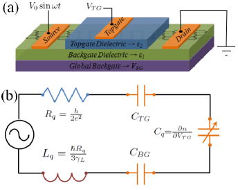
A schematic representation of the device under consideration and a biasing scheme are shown in Figure 1a. The device consists of a narrow graphene nanoribbon of width , with Ohmic source and drain contacts and capacitively coupled back and top gates, which are electrically isolated from the GNR by two dielectrics with permettivities and . A thin metallic top gate is utilized to provide a locally tunable barrier via the application of an electrostatic bias , whereas a global bias may be applied to the backgate , which is used to modulate the Fermi level in the entire device. Furthermore, the top gate potential is used to electrostatically define a quantum dot (QD). Similar devices are routinely fabricated Huang et al. (2007); Stander, Huard, and Goldhaber-Gordon (2009), and transport in this structures has been studied in both DC Stander, Huard, and Goldhaber-Gordon (2009); Young and Kim (2009) and more recently low frequency AC Lin et al. (2009) bias regimes. In our discussion we assume that only a single level of the QD is accessible to electrons in the source-drain bias window so that the dot can be characterized by a single energy level and line width .
In order to explore transport through this device in both DC and high frequency AC regimes, we utilize the Green-Kubo formalism to calculate the frequency dependent admittance through the QD using
| (1) |
where is the topgate length, is the current operator, and is a positive infinitesimal. The admittance for the top gate defined quantum dot, which we denote as is evaluated in Appendix I. Furthermore, in order to couple the high frequency admittance of the QD to the GNR device, we utilize the method introduced by Wang et al Wang, Wang, and Guo (2007):
| (2) |
where, is the total geometric capacitance, and is the quantum capacitance of the nanoribbon, which is proportional to the density of states at the Fermi energy. The frequency dependent electrochemical capacitance is related to the admittance of the entire device by .
II.1 Quantum Inductance
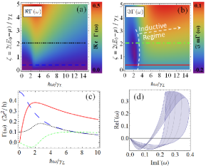
In order to interpret the physical meaning of the complex QD admittance , we express it in terms of its real and imaginary components (see Appendix I for the complete expression). Similar expressions for the admittance are obtained in Wang, Wang, and Guo (2007, 1999) using a nonequilibrium Green’s function approach. We further introduce a dimensionless parameter (see Appendix I) in order to characterize the width of the resonance, where is the electrochemical potential of the source lead, and the difference defines the transport window created by the source-drain bias. In the limit , we recover the DC Landauer conductivity . A plot of both real and imaginary components of the dynamic admittance are shown in Appendix I. As can be seen in Fig. 7b, the sign of the imaginary component of the admittance becomes positive after a critical transition frequency , corresponding to a negative capacitance, or, equivalently, to inductive behavior. It should be noted that in quantum transport the sign convention is opposite to the one used in electrical engineering. Namely, the sign of the frequency component is chosen such that corresponds to inductive behavior. Quantum inductance in various nanostructures has been previously investigated both theoretically Yam et al. (2008); Wang, Wang, and Guo (2007); Fu and Dudley (1993) and verified experimentally Gabelli et al. (2006).
Phenomenologically, the inductive behavior of the QD can be understood by viewing the QD and topgate as forming a parallel plate capacitor. In classical parallel plate capacitors, charge accumulation on the device results from the application of a voltage. However, even for a quantum coherent capacitor there exists an intrinsic charge relaxation resistance , in the limit of a single transport channel Gabelli et al. (2006); Nigg, Lopez, and Büttiker (2007). Consequently, the charge accumulation time is . If the driving voltage is an AC signal, the charge accumulation will follow the voltage and will also reverse sign in due time . Ideally, in the absence of resistance, there is a phase lag between the current and the AC driving voltage. This is only true for low frequency AC signals. For high frequencies , the charge buildup cannot follow the changes in the AC voltage. This situation gives rise to an effective negative capacitance, or inductive behavior, since in this transport regime it appears as though the voltage on the plates lags the current, as shown in the parametric plot of the amplitude-phase diagram in Fig. 7d. It should be noted that this effect arises from the presence of a quantum mechanical charge relaxation resistance, , and is therefore quantum mechanical in origin. Consequently, quantum mechanical devices exhibit inductive behavior at sufficiently high frequencies even though no geometric inductor is present in the circuit.
It was further pointed out Wang, Wang, and Guo (2007), that a second relevant time scale in high frequency transport of QDs is introduced by the carrier dwell time of the QD, which is related to the line width function of the dot barrier . Smaller serves the purpose of increasing the charge carrier dwell time inside the QD region and consequently lowering the transition frequency at which quantum inductance appears. For sufficiently small (i.e., large dwell times), the transport is always inductive, even at low frequencies; however, these regimes have not yet been realized experimentally due to the difficulty that arises in fabricating strongly coupled topgate leads. Utilizing the above considerations, Wang et al., Wang, Wang, and Guo (2007) define the quantum inductance as . In essence, the finite line width forces a charge carrier to remain inside the dot for at least time implying that the charge carriers can only follow changes in the voltage for frequencies . At higher frequencies this effective trapping of the charges inside the QD for gives rise to such large phase delays between the current and voltage that the capacitance appears negative. In our system, this dwell time effect is larger than the charge relaxation time, so that the inductive behavior is attributable to the trapping of charge carriers in the QD.
II.2 Quantum Capacitance
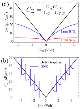
Unlike quantum inductance which is does not depend on graphene’s particular density of states, quantum capacitance, introduced by S. Luryi Luryi (1988), depends on the underlying band structure of the material. The quantum capacitance describes the movement of the conduction band as a function of the applied gate bias: . Unlike in most conventional semiconductors, in graphene, the quantum capacitance is an important parameter since in the low bias regime, monolayer graphene exhibits a linear gate tunable dispersion Sarma et al. ; Chen and Appenzeller (2008); Fang et al. (2007). In the case of narrow constrictions, when the GNR width approaches the Fermi wavelength of the electrons, a bandgap opens Han et al. (2007) and (as well as the density of states) exhibit van Hove singularities, as shown in Fig. 2b Fang et al. (2007). Consequently the quantum capacitance of a graphene nanoribbon (per unit width) can also be tuned by varying the gate bias according to
| (3) |
where , is the energy of the subband, and is the Heaviside step function. The expression for the quantum capacitance of graphene stated in Eq. 3 is the same as the one obtained by other authors Fang et al. (2007), and it’s derivation is outlined in Appendix II. We can combine the geometric capacitances of the gates and the quantum capacitance of the GNR to form the total capacitance
Since current graphene-based devices are fabricated using relatively thick backgate dielectrics (typically on the orders of hundreds of nanometers), , consequently, has no contribution to . We therefore only need to take into account the contribution from the topgate dielectric and can ignore the capacitive contribution from the backgate and the capacitive coupling to the contacts, which cannot be tuned by a gate bias. Although the capacitive coupling to the backgate and contacts changes the value of the geometric capacitance, which in turn decreases the voltage range over which can be modulated (a similar effect is achieved in Fig. 2a by changing the dielectric constant of the top gate), gate modulation of the total capacitance has been experimentally observed Xia et al. (2009); Henriksen and Eisenstein (2010). The total capacitance is then determined by, . The contribution of the quantum capacitance dominates in the limit of small quantum capacitance , i.e., in devices with thin gate dielectrics since it is in series with the geometric capacitance, and for capacitors in series, the smaller capacitance dominates Chen and Appenzeller (2008); Fang et al. (2007); Xia et al. (2009); Giannazzo et al. (2009). In typical GNR devices the oxide capacitance is on the order of Huard et al. (2007) and the trap capacitance, , which arises from the coupling to the leads is on the order of . while the quantum capacitance can be tuned in the range Chen and Appenzeller (2008). Figure 2a shows the total capacitance as a function of several typical dielectric materials. The quantum capacitance of a 2.5 nm GNR is shown in Fig 2b. While optical properties and carrier transport in GNR’s are in general affected by the particular graphene edge state such as armchair, zigzag, or mixed edges Begliarbekov et al. (2010a), for simplicity we consider GNRs with pure armchair boundaries Zheng et al. (2007).
II.3 Fano Factor
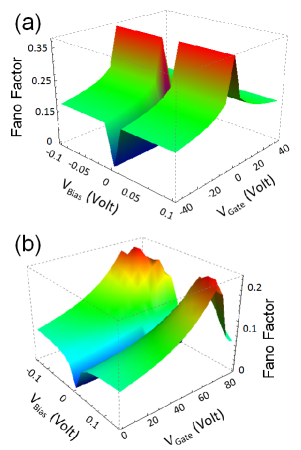
In order to compare our model with previous experimental work, we note that the real part of Eq. 1 is proportional to the frequency dependent shot noise Djuric and Search (2006); Buttiker, Pretre, and Thomas (1993). Consequently, our model can be utilized to calculate the frequency dependent Fano factor of a graphene nanoribbon. The dependence of the Fano factor of a GNR on gate and source-drain bias at MHz is plotted in Figure 3. The device parameters, such as the dielectric thickness, GNR aspect ratio ( with ) and operating frequency were chosen to match existing experimental results Danneau et al. (2008a, b). The resultant dependence of the Fano factor is in excellent agreement with the measured values. Experimentally, the Fano factor peaks at a value , while in our model it peaks at Furthermore, the change in slope of the Fano factor occurs at in both the experimental data and in our calculation. Although, in our calculation the Fano plot is symmetric about , this is not the case in the experimental data. This discrepancy is caused by the shift of the Dirac point in the presence of charged impurities Tan et al. (2007); Begliarbekov et al. (2010b). The slight discrepancy between Fig. 3a and the measured value at zero gate bias and the theoretical prediction most likely stems from a finite density of states at the Dirac point, which is a feature measured in numerous experiments Droscher et al. (2010). Although the above simulations model a relatively wide GNR, since the real part of the frequency dependent admittance, is proportional to the frequency dependent shot noise, the agreement between the experimental data and our model point to its validity. However, further experiments are needed for smaller GNRs at higher frequency to fully assess the theoretical predictions.
III Results & Discussion
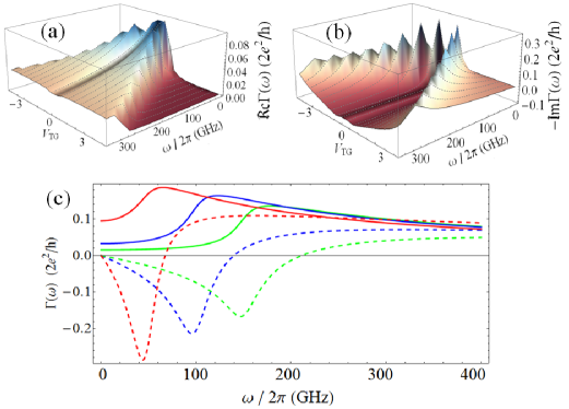
We now turn to the discussion of our main result, the dynamic admittance of the top gated GNR. The real and imaginary components of are plotted in Figure 4. Figure 4b, shows the imaginary component of the admittance as a function of frequency and the top gate bias (the sign of the imaginary admittance has been inverted for clarity) where one can see that becomes negative, corresponding to an inductive behavior of the device. The spikes in correspond to resonances between the electronic states inside the QD and the van Hove singularities of the GNR. Off-resonant cases are plotted if Fig. 4c. In general, the width of the GNR changes the energy spacing of the van Hove singularities. For a GNR with W=2.5nm, the spacing is ~1V (see Fig. 2b), while for 5 nm GNR the energy spacing decreases to ~0.4V Fang et al. (2007). Consequently, in order to achieve the desired resonance source-drain voltages below the energetic spacing of the van Hove singularities should be selected, in our case . Larger source drain volrages (or equivalently wider GNRs) would result in several van Hove peaks being inside the transport window. If a sufficiently small number of resonance levels (2 or 3) are present in the transport window, the sharp resonances in the conductance are no longer visible, however the general features of the complex admittance are still present. For a larger number of resonant levels, the transport becomes diffusive, and the effect of quantum inductance is no longer observed.
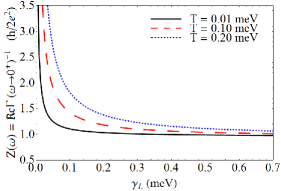
In the limit and large the real part of the frequency dependent impedance approaches the charge relaxation resistance as shown in Figure 5. For small values of , diverges since low values of the line width function correspond to large values of the carrier dwell times , for which transport through the QD becomes blocked.
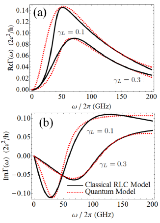
For frequencies greater than where , the transport through the GNR crosses over from being purely capacitive to RLC behavior and the admittance of the device can modeled by a classical series RLC circuit as
The comparison of the classical RLC model to the quantum model is shown in Fig. 6. In the above model, the circuit inductance of the GNR is given by and . In accordance with the model proposed by Wang et al. for a generic quantum dot Wang, Wang, and Guo (2007), the transition frequency in our device occurs below the resonance frequency . The transition frequency is determined by the carrier dwell time (or equivalently and ranges from 50 - 200 GHz for the values of shown in Fig. 4, which corresponds to inductances of 40 - 200 nH. Furthermore, the resonance frequency of the resultant RLC circuit is given by . Using the above inductance values, for typical quantum dot sizes of 100 nm2 and 25 nm2 fabricated on 300 nm SiO2 with a capacitance of 11.5 nF / cm2 and 30 F/cm2 quantum capacitance of graphene, we predict resonant frequencies of this oscillator on the order of 100 - 900 GHz. This gives rise to Q-factors on the order of Q = - ( is the width of the resonance). This is a remarkable number for an all electronic circuit. To compare this result to conventional 2DEG structures, such as AlGaAs heterojunctions, we note that the dwell time may be approximated as Wang, Wang, and Guo (2007), where is the device length and is the Fermi velocity. Since is AlGaAs 2DEGs is typically on the order of , the corresponding Quantum inductance and Q factor would be an order of magnitude lower. It should be noted that the above results were obtained assuming prestine nanoribbons, and effects that would lead to dephasing or the degradation of the ballistic mean free path, such as the morphology Liu and Yakobson (2010) of the device and potential fluctuations have not been considered and are beyond the scope of this study. In general, spatial potential fluctuations in graphene are on the order of tens of meV Du et al. (2008), while the typical values of are on the order of eV. The average size of the potential fluctuations was measured to be ~30 nm Martin et al. (2008). Consequently, if the topgate length is smaller than the size of the potential fluctuations (such as the case with Si nanowires and carbon nanotube electrodes), the size of the potential would be constant and would not affect the result. Furthermore eV corresponds to a dwell time of 260ps. Therefore, temporal potential fluctuations that are the same order of magnitude as the dwell time could potentially lead to a loss of coherence. However, if the GNR is fabricated on Boron Nitride dielectrics Dean et al. (2010) or is suspended Du et al. (2008) the undesired effects of potential fluctuations are largely reduced.
The large Q-factor and in-situ tunability of the quantum capacitance afforded by shifting the gate bias makes this device ideal for ultra-high frequency electronic applications. Commercially available high frequency electronic circuits are not capable of operating frequencies higher than 40 GHz. However, the proposed device architecture, would extend the operating frequency of all-electronic devices into the terahertz regime. For example, if a high frequency AC signal is applied to the source-drain contacts, a subsequent sweep of the top gate voltage would drive the oscillator in and out of resonance, allowing for an all electronic measurement of this frequency via the device gain. Consequently, a measurement of the on and off resonant gain in the device yields an all electronic measurement of the frequency of the signal. Since is on the order of 100+ GHz, this GNR-RLC circuit could be used to measure frequencies which are currently unattainable by standard instrumentation. This, coupled with graphene’s intrinsically ultra-high carrier mobilities, render it an ideal material for all-electronic THz devices.
IV Conclusion
In conclusion, we have applied the Green-Kubo formalism to model high frequency transport through dual gated graphene nanoribbons. We showed that above a sufficiently high frequency determined by the dwell time of charge carriers in the gate-defined quantum dot, the behavior of the GNR device is analogous to a classical RLC oscillator with a very high Q-factor. The inductive behavior arises from the negative capacitance of the QD which occurs when charge carriers become trapped inside the dot for times and cannot follow the driving voltage. This leads to a phase lag greater than and thus results in a negative capacitance. Coupling the inductive behavior of a quantum dot to the gate tunable quantum capacitance in graphene, gives rise to an in-situ tunable ultra high frequency oscillator and filter thereby extending the reach of high frequency electronics into the THz regime.
Acknowledgements.
M.B. acknowledges partial financial support for this work that was provided by the NSF GK-12 Grant No. NSF DGE-0742462 and S.S. acknowledges support from the Air Force Office for Scientific Research (award no FA9550-08-1-0134). C.P.S acknowledges support from NSF Grant. No. 0757933.Appendix I
Here we derive the complex admittance for a QD with a single resonant level. We emphasize that these results are general for any QD and are not specific to graphene. Following the procedure in Fu and Dudley (1993), the expression in Eq. 1 for the admittance may be expressed in terms of transmission and reflection amplitudes as
| (4) |
where is the Fermi function. The transmission and reflection amplitudes through the barrier are given by
| (5) |
where is a linewidth function representing the coupling of the lead to the QD and characterize the energy width of the resonance Fu and Dudley (1993). The linewidth function of the lead is related to the carrier dwell time, , inside the QD according to
Substituting Eq. 5 into Eq. 4 and carrying out the integrations, we obtain the following result for the dynamic impedance of the QD :
| (6) |
The real and imaginary components of are plotted in Figure 7 as a function of the dimensionless parameter (see main text for discussion).
Appendix II
In this section we provide a brief derivation of the quantum capacitance, . To do so we require an energy dependent expression for the density of states. This is computed in the Landauer-Bttiker formalism. In the low bias regime the ballistic conductance is given by
where is the Fermi function. In the ballistic limit . Furthermore, the mode function is given by
where is the group velocity given by Using this, we can express the mode function as
which becomes,
where the factor 2 is introduced to account for spin degeneracy. Inserting the above expression for into , and making use of the fact that, we obtain
Integrating the above expression by parts, and doing some algebra, we obtain
where is the Gamma function, is the Fermi-Dirac Integral given by , and . Taking the low temperature limit we have , in which case the expression for the ballistic conductivity reduces to
These results can now be used to calculate the quantum capacitance of a graphene strip defined as Following the same procedure as above, the carrier densities are given by
which is in agreement with literature Fang et al. (2007). Using this expression, and differentiating it at the Fermi energy, we obtain
which in the low temperature limit, can be shown to be
This result can be further generalized to a case of a realistic GNR of finite width, yielding Eq. 3 in the text.
References
- Novoselov et al. (2004) K. Novoselov, A. Geim, S. Morozov, D. Jiang, Y. Zhang, S. Dubonos, I. Grigorieva, and A. Firsov, Science 306, 666 (2004).
- Zhang et al. (2005) Y. B. Zhang, Y. W. Tan, H. L. Stormer, and P. Kim, Nature 438, 201 (2005).
- Novoselov et al. (2007) K. S. Novoselov, A. K. Geim, S. V. Morozov, D. Jiang, M. I. Katsnelson, I. V. Grigorieva, S. V. Dubonos, and A. A. Firsov, Nature 438, 197 (2007).
- Li and Andrei (2007) G. Li and E. Y. Andrei, Nature Physics 3, 623 (2007).
- Du et al. (2009) X. Du, I. Skachko, F. Duerr, A. Luican, and E. Y. Andrei, Nature 462, 192 (2009).
- Bolotin et al. (2009) K. I. Bolotin, F. Ghahari, M. D. Shulman, H. L. Stormer, and P. Kim, Nature 462, 196 (2009).
- Huard et al. (2007) B. Huard, J. A. Sulpizio, N. Stander, K. Todd, B. Yang, and D. Goldhaber-Gordon, Physical Review Letters 98, 236803 (2007).
- Du et al. (2008) X. Du, I. Skachko, A. Barker, and E. Y. Andrei, Nature Nanotech. 3, 491 (2008).
- Dean et al. (2010) C. R. Dean, A. F. Young, I. Meric, C. Lee, L. Wang, S. Sorgenfrei, K. Watanabe, T. Taniguchi, P. Kim, K. L. Shepard, and J. Hone, Nature Nano. 5, 722 (2010).
- Miao et al. (2007) F. Miao, S. Wijeratne, Y. Zhang, U. C. Coskun, W. Bao, and C. N. Lau, Science 317, 1530 (2007).
- Wang et al. (2008) X. R. Wang, Y. J. Ouyang, X. L. Li, H. L. Wang, J. Guo, and H. J. Dai, Physical Review Letters 100, 206803 (2008).
- Balandin et al. (2008) A. A. Balandin, S. Ghosh, W. Z. Bao, I. Calizo, D. Teweldebrhan, F. Miao, and C. N. Lau, Nano Letters 8, 902 (2008).
- Lee et al. (2008) C. Lee, X. D. Wei, J. W. Kysar, and J. Hone, Science 321, 385 (2008).
- Lu, Ocola, and Chen (2009) G. H. Lu, L. E. Ocola, and J. H. Chen, Applied Physics Letters 94, 083111 (2009).
- Moradian, Mohammadi, and Ghobadi (2008) R. Moradian, Y. Mohammadi, and N. Ghobadi, Journal of Physics-condensed Matter 20, 425211 (2008).
- Huang et al. (2007) C. W. Huang, Y. T. Wu, C. C. Hu, and Y. Y. Li, Journal of Power Sources 172, 460 (2007).
- Lin et al. (2010a) Y. M. Lin, C. Dimitrakopoulos, K. A. Jenkins, D. B. Farmer, H. Y. Chiu, A. Grill, and P. Avouris, Science 327, 662 (2010a).
- Emtsev et al. (2009) K. V. Emtsev, A. Bostwick, K. Horn, J. Jobst, G. L. Kellogg, L. Ley, J. L. McChesney, T. Ohta, S. A. Reshanov, J. Rohrl, E. Rotenberg, A. K. Schmid, D. Waldmann, H. B. Weber, and T. Seyller, Nature Materials 8, 203 (2009).
- Ryzhii et al. (2009) V. Ryzhii, M. Ryzhii, A. Satou, T. Otsuji, A. A. Dubinov, and V. Y. Aleshkin, Journal of Applied Physics 106, 084507 (2009).
- Wright, Cao, and Zhang (2009) A. R. Wright, J. C. Cao, and C. Zhang, Physical Review Letters 103, 207401 (2009).
- http://www.itrs.net/ Links/2009ITRS/Home2009.htm (2009) http://www.itrs.net/ Links/2009ITRS/Home2009.htm, (2009).
- (22) S. D. Sarma, S. Adam, E. H. Hwang, and E. Rossi, arXiv:1003.4731 .
- Lin et al. (2009) Y. M. Lin, K. A. Jenkins, A. Valdes-Garcia, J. P. Small, D. B. Farmer, and P. Avouris, Nano Lett. 9, 422 (2009).
- Lin et al. (2010b) Y. M. Lin, C. Dimitrakopoulos, K. A. Jenkins, D. B. Farmer, H. Y. Chiu, A. Grill, and P. Avouris, Science 327, 662 (2010b).
- Stander, Huard, and Goldhaber-Gordon (2009) N. Stander, B. Huard, and D. Goldhaber-Gordon, Physical Review Letters 102, 026807 (2009).
- Young and Kim (2009) A. F. Young and P. Kim, Nat. Phys. 5, 222 (2009).
- Wang, Wang, and Guo (2007) J. Wang, B. Wang, and H. Guo, Phys. Rev. B. 75, 155336 (2007).
- Wang, Wang, and Guo (1999) B. Wang, J. Wang, and H. Guo, Phys. Rev. Lett. 82, 398 (1999).
- Yam et al. (2008) C. Yam, YanMo, FanWang, X. Li, G. Chen, X. Zheng, Y. Matsuda, J. Tahir-Kheli, and W. A. G. III, Nanotechnology 19, 495203 (2008).
- Fu and Dudley (1993) Y. Fu and S. C. Dudley, Phys. Rev. Lett 70, 65 (1993).
- Gabelli et al. (2006) J. Gabelli, G. Feve, J.-M. Berroir, B. Placais, A. Cavanna, B. Etienne, Y. Jin, and D. C. Glattli, Science 313, 499 (2006).
- Nigg, Lopez, and Büttiker (2007) S. E. Nigg, R. Lopez, and M. Büttiker, Phys. Rev. Lett 97, 206804 (2007).
- Danneau et al. (2008a) R. Danneau, F. Wu, M. F. Craciun, S. Russo, M. Tomi, J. Salmilehto, A. F. Morpurgo, and P. J. Hakonen, Phys. Rev. Lett 100, 196802 (2008a).
- Danneau et al. (2008b) R. Danneau, F. Wu, M. F. Craciun, S. Russo, M. Y. Tomi, J. Salmilehto, A. F. Morpurgo, and P. J. Hakonen, J. Low Temp. Phys. 153, 374 (2008b).
- Luryi (1988) S. Luryi, Appl. Phys. Lett. 52, 6 (1988).
- Chen and Appenzeller (2008) Z. Chen and J. Appenzeller, in IEDM Technical Digest (2008) pp. 509–512.
- Fang et al. (2007) T. Fang, A. Konar, H. Xing, and D. Jenaa, Appl. Phys. Lett. 91, 092109 (2007).
- Han et al. (2007) M. Y. Han, B. Ozyilmaz, Y. Zhang, and P. Kim, Phys. Rev. Lett. 98, 206805 (2007).
- Xia et al. (2009) J. Xia, F. Chen, J. Li, and N. Tao, Nature Nanotechnology 4, 505 (2009).
- Henriksen and Eisenstein (2010) E. A. Henriksen and J. P. Eisenstein, Phys. Rev. B 82, 041412(R) (2010).
- Giannazzo et al. (2009) F. Giannazzo, S. Sonde, V. Raineri, and E. Rimini, Nano Lett. 9, 23 (2009).
- Begliarbekov et al. (2010a) M. Begliarbekov, O. Sul, S. Kalliakos, E.-H. Yang, and S. Strauf, Appl. Phys. Lett. 97, 031908 (2010a).
- Zheng et al. (2007) H. Zheng, Z. F. Wang, T. Luo, Q. W. Shi, and J. Chen, Phys. Rev. B 75, 165414 (2007).
- Djuric and Search (2006) I. Djuric and C. P. Search, Phys. Rev. B 74, 115327 (2006).
- Buttiker, Pretre, and Thomas (1993) M. Buttiker, A. Pretre, and H. Thomas, Physical Review Letters 70, 4114 (1993).
- Tan et al. (2007) Y.-W. Tan, Y. Zhang, K. Bolotin, Y. Zhao, S. Adam, E. H. Hwang, S. D. Sarma, H. L. Stormer, and P. Kim, Physical Review Letters 99, 246803 (2007).
- Begliarbekov et al. (2010b) M. Begliarbekov, O. Sul, N. Ai, E.-H. Yang, and S. Strauf, Appl. Phys. Lett. 97, 122106 (2010b).
- Droscher et al. (2010) S. Droscher, P. Roulleau, F. Molitor, P. Studerus, C. Stampfer, K. Ensslin, and T. Ihn, Appl. Phys. Lett. 96, 152104 (2010).
- Liu and Yakobson (2010) Y. Liu and B. I. Yakobson, Nano. Lett. 10, 2178 (2010).
- Martin et al. (2008) J. Martin, N. Akerman, G. Ulbricht, T. Lohmann, J. H. Smet, K. V. Klitzing, and A. Yacoby, Nature Physics 4, 144 (2008).