Phase Diagram of Electrostatically Doped SrTiO3
Abstract
Electric double layer transistor configurations have been employed to electrostatically dope single crystals of insulating SrTiO3. Here we report on the results of such doping over broad ranges of temperature and carrier concentration employing an ionic liquid as the gate dielectric. The surprising results are, with increasing carrier concentration, an apparent carrier-density dependent conductor-insulator transition, a regime of anomalous Hall effect, suggesting magnetic ordering, and finally the appearance of superconductivity. The possible appearance of magnetic order near the boundary between the insulating and superconducting regimes is reminiscent of effects associated with quantum critical behavior in some complex compounds.
Strontium Titanate (STO) is a band insulator which has been rendered conducting and superconducting at sufficiently low temperatures by introducing oxygen defects, by doping with Nb, Zr, La, or TaKoonce ; Binnig ; Hulm ; Suzuki ; Olaya ; Gurvitch ; Leighton , through charge transfer processes resulting from the deposition of several layers of LaAlO3Reyen , by electrostatic charging using a conventional field effect transistor (FET) configuration Nakamura , and by charging using an electric double layer transistor (EDLT) configuration employing a polymer electrolyteUeno . In this letter we report the results of an electrostatic charging experiment on SrTiO3 using an ionic liquid (IL) in an EDLT configuration, which has revealed unexpected features in the phase diagram as a function of temperature and carrier concentration, resembling those in the phase diagrams of unconventional superconductors, or systems exhibiting quantum critical behavior Taillefer ; SI .
EDLTs are configurations which perform in a manner similar to conventional FETs. They contain a gate electrode, a semiconductor or insulator into which charge can be accumulated or depleted, source and drain electrodes, and for purposes of characterization, electrodes for measuring longitudinal and transverse voltages relative to the current direction. In this instance the gate dielectric is an IL, although polymer electrolytes have also been employed. ILs are molten salts consisting of large ions such that their Coulomb interaction is sufficiently small to make them room temperature liquids. They have previously been used to modify the conductivity of ZnO, and ZrNCl, revealing a metal-insulator transition in ZnO, and superconductivity in ZrNClMisra ; Shimotani ; Ye ; Hongtao Yuan . Upon applying a gate voltage, ions move to the surface of the semiconductor or insulator, forming an electric double layer (EDL) such that with the charge induced in the channel, acts as a capacitor of nanoscale thickness. A schematic of the operation of an EDLT is shown in Fig. 1. With ILs, charge transfers of order 1014 cm-2 or higher are possible, opening up the possibility of significant modification of the electronic properties of materialsAhn . The advantage of using ILs over almost most solid gate dielectrics is a greatly enhanced charge transfer for the same gate voltage.
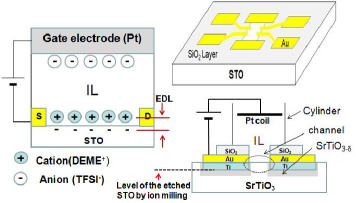
Pristine STO (100) single-crystals were obtained from Princeton Scientific Corp. Their surfaces were treated with buffered hydrofluoric acid for 30 seconds and annealed at 780∘C for 6 hours to yield an atomically flat surface terminated by TiO2Kawasaki . Electrodes in a typical Hall bar geometry along with a four-probe configuration for measuring longitudinal resistance were pre-patterned by means of photolithography as shown in Fig. 1. Prior to the deposition of Ti/Au electrodes (each layer, 70 nm in thickness), the STO was ion milled to a depth of 70nm to create a layer of oxygen-deficient metallic SrTiO3-δ. The depth of milling of the STO is shown in Fig. 1. Milling was carried out to insure ohmic contact between the Ti/Au electrodes and the surface layer of STO that would be electrostatically gated into a conductive stateReagor . Next a 100nm thick layer of SiO2 was deposited through a photo-patterned mask onto the STO to define a conducting channel in area. The IL used here was N,N-diethyl-N-(2-methoxyethyl)-N-methylammonium bis (trifluoromethyl sulphonyl)-imide (DEME-TFSI). This particular IL has produced very high charge accumulations on the surface of semiconductors such as ZnO with induced sheet carrier densities () of up to being reported Hongtao Yuan . Moreover the ions of this IL are mobile down to 200K. The ability to apply a gate voltage,, at this relatively low temperature enables us to raise voltage as high as 5V without significant and irreversible chemical degradation that would occur at higher temperatures.
Four-probe measurements were employed to determine the resistance of samples. A Quantum Design Physical Property Measurement System (PPMS) equipped with a 3He refrigerator insert enabled us to vary the temperature between 300K and 0.35K and the magnetic field between 0T and 9T. As the IL, DEME-TFSI, undergoes a rubber-like phase transition below 240K and becomes a glass-like solid below 200K, where the ionic mobility falls to zeroHongtao Yuan . was always changed at 230K. and ranged from 0V to 3V. It was applied using a Keithley electrometer (Model 6517A), and was held constant throughout subsequent cooling and measurement.
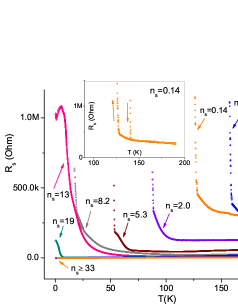
The temperature dependencies of the sheet resistances , of an STO crystal at various values of are plotted in Fig. 2. Undoped STO exhibited no measurable conductivity, and only with in excess of 1.8V was it possible to measure nonzero conductivity. Within a given cycle of cooling and warming at a fixed value of there was no more than a 5 to 10% shift in resistance when the crystal was brought back to 230K. In a set of independent measurements using this IL, the value of the capacitance in a parallel plate configuration exhibited a small time dependence, owing to the complex dynamics of the IL in its glassy stateRivera ; Jacob Stevenson . Areal carrier density, , rather than , is the intrinsic parameter. Values of were obtained from Hall effect data at 180K, which was measured in magnetic fields , of up to 5T, and ranged from to The highest value of ever induced was . The areal carrier concentration, , was not linear in , which is probably a consequence of the voltage dependence of the IL’s dielectric properties.
In most plots of , we observed a sharp resistance rise at a temperature which depended upon which was not instrumental. This could be due to the reduction of carriers thermally excited from states within the band gap, when decreasing the temperature. Such an effect is believed to be responsible for the temperature dependence of the voltage threshold for conductance as has been found in various oxide FETsTaisuke . However, the sharpness of the rise in , and the fact that it is hysteretic, as shown in the inset of Fig. 2, strongly suggest that this behavior to be the signature of a first order phase transition in the layer that is electrostatically doped.
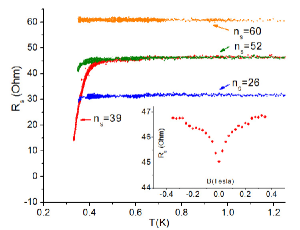
It is well known that chemically doped STO, exhibits superconductivity at relatively low bulk carrier densities Koonce . Recently EDLT configurations were used to induce superconductivity in an undoped insulating STOUeno . In the present work, we were able to produce a very similar result albeit with a different dielectric. The onset of a superconducting transition was observed at a temperature of about 0.4K at (measured at 0.5K). Superconductivity either disappears or is just shifted to lower temperatures, no more accessible with our set up, as we increased the value of . Data exhibiting the onset of superconductivity is shown in Fig. 3.
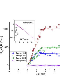
In Fig. 4. we plot vs. , the Hall resistance vs. with the ordinary Hall Effect (OHE) term, subtracted. This linear term was obtained from a fit to the high field limit with . A deviation from the linearity of the Hall resistance vs. magnetic field, known as anomalous Hall effect (AHE), is observed. Similar effects have been reported at the SrTiO3/LaAlO3 interface BenShalom ; Snir Seri ; C. Bell . The AHE can result from a multiple band structureC. Bell and/or a magnetization induced by external field BenShalom ; Snir Seri . The observation that the Hall resistance changes at low magnetic fields and saturates at some high field, favors the magnetization scenario. The AHE effect was not observed at temperatures of 90 K and above, as shown in the inset of Fig. 4.
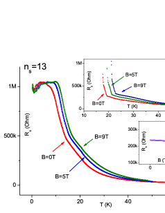
The magnetic field-dependence of in the region where an AHE was observed was also investigated. Examples are shown in Fig. 5. The peak at shifted to higher temperatures upon the application of a magnetic field and the response to field was not hysteretic. Similar behavior was found at the somewhat lower carrier density of (the upper-right inset of Fig. 5). This effect disappeared for carrier densities of and lower (lower-right inset). We suspect this effect is associated with magnetic order. It should be noted that ferromagnetic order of the electron spins within the Ti-3d conduction band was predicted for both LaTiO3/SrTiO3 and LaAlO3/SrTiO3 interfacesPentcheva ; Okamoto and evidence for this was presented by A. Brinkman et al.Brinkman in the form of hysteretic magnetoresistance curves. In the present work there is no hysteresis. Consequently it is not certain that ferromagnetism is responsible for the observed phenomena.
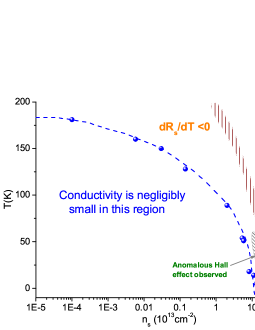
Lastly, we have drawn a tentative phase diagram in the space of and , summarizing our observations (Fig. 6). Due to the limited temperature range of the PPMS, it is not certain that there exists a dome-like feature for the variation of the superconducting transition temperature with , analogous to the result found for chemically-doped, bulk STOKoonce .
In summary, we have found a series of different behaviors of electrostatically doped STO with the doping carried out using an EDLT configuration. We have documented the systematic decrease of the temperature of carrier freeze-out with increasing carrier concentration, with this apparent conductor-insulator transition disappearing when superconductivity turns on. The appearance of a peak in , which is magnetic field dependent, in the vicinity of this crossover to superconductivity, along with an anomalous Hall effect suggests the possibility of a magnetic phase in the crossover regime. This is reminiscent of what is found near quantum critical points in strongly correlated electron systemsSI . Lower temperature measurements may elucidate the precise behavior. An open question is the actual depth of penetration of the induced charge layer. Recent theoretical work suggests that it may be localized within a very narrow layer on the order of one lattice constant rather than some greater distanceShklovskii . If that is indeed the case then the properties revealed in this work need not be analogous to those found in bulk doping experiments.
We would like to thank Yen-Hsiang Lin and Christopher Leighton for fruitful discussions and advice. This work was supported by the NSF under Grant No. NSF/DMR-0854752 and by the DOE under grant No. ED-FG02-02ER46004. Part of this work was carried out at the University of Minnesota Characterization Facility, a member of the NSF-funded Materials Research Facilities Network via the MRSEC program, and the Nanofabrication Center which receive partial support from the NSF through the NNIN program.
References
- (1) C. S. Koonce, Marvin Cohen, J. F. Schooley, W. R. Hosler, and E. R. Peiffer, Phys. Rev. 163, 380 (1967).
- (2) G. Binnig, A. Baratoff, H.. E. Hoenig, and J. G. Bednorz, Phys. Rev. Lett. 45, 1352 (1980).
- (3) J. K. Hulm, C. K. Jones, R. C. Miller and T. Y. Tien, in Proceedings of the Tenth International Conference on Low–Temperature Physics, Moscow, 1966, edited by M. P. Malkov (Proizvodstrenno-Izdatel’skii Kombinat, VINITI, Moscow, 1967) Vol IIA, pp 86-114.
- (4) H. Suzuki et al., J. Phys. Soc. Jpn. 65, 1529 (1996).
- (5) David Olaya, Feng Pan, Charles T. Rogers, and John C. Price, Appl. Phys. Lett. 84, 4020 (2004).
- (6) M. Gurvitch, H. L. Stormer, R. C. Dynes, J. M. Graybeal, and D. C. Jacobsen, in Extended Abstracts: Superconducting Materials. Proceedings of Symposium S, 1986 Fall Meeting of the Materials Research Society, 3 – 5 December 1986, Boston, MA, edited by J. Bevk and A. I Braginski (Materials Research Society, Pittsburgh, 1987), p 47.
- (7) A. Spinelli, M. A. Torija, C. Liu, C. Jan, and C. Leighton, Phys. Rev. B. 81, 155110 (2010).
- (8) N. Reyen et al., Science 317, 1196 (2007); Mark Huijben, Alexander Brinkman, Gertjan Koster, Guus Rijnders, Hans Hilgenkamp, and Vad H. A. Blank, Adv. Mater. 21, 1665 (2009).
- (9) H. Nakamura, H. Takagi, I. H. Inoue, Y. Takahashi, T. Hasegawa, and Y. Tokura, Appl. Phys. Lett. 89, 133504 (2006).
- (10) K. Ueno et al., Nature Materials 7, 855 (2008).
- (11) Louis Taillefer, arXiv:1003.2972; Annual Review of Condensed Matter Physics 1, 51 (2010).
- (12) Philipp Gengenwart, Qimiao Si and Frank Steglich, Nature Physics 4, 186 (2008).
- (13) Rajiv Misra, Mitchell McCarthy and Arthur F. Hebard, Appl. Phys. Lett. 90, 052905 (2007).
- (14) H.Shimotani et al., Appl. Phys. Lett. 91, 082106 (2007).
- (15) J. T. Ye et al., Nature Materials 9, 125 (2010).
- (16) C. H. Ahn et al., Rev. Mod. Phys. 78, 1185 (2006).
- (17) M. Kawasaki et al., Science 266, 2540 (1994).
- (18) D. Reagor et al., Nature Material 4, 593 (2005).
- (19) Alberto Rivera and Ernst A. Rossler, Phy. Rev. B. 73, 12201 (2006).
- (20) Jacob D. Stevenson and Peter G. Wolynes, Naure Physics 6, 62 (2009).
- (21) Hongtao Yuan et al., Adv. Funct. Mater. 19, 1046 (2009).
- (22) Taisuke Sato et al., Japanese J. of Appl. Phys. 46, L515 (2007); K. Ueno et al., Appl. Phys. Lett. 84, 3726 (2004).
- (23) S. Okamoto, A. J. Millis, A. J. and N. A. Spaldin, Phys. Rev. Lett. 70, 2126 (2006).
- (24) R. Pentcheva and W. E. Pickett, Phys. Rev. B 74, 035112 (2006).
- (25) A. Brinkman et al., Nature Materials 6, 493 (2007).
- (26) M. Ben Shalom et al., Phys. Rev. Lett. 104, 126802 (2010).
- (27) C. Bell et al., Phys. Rev. Lett. 103, 226802 (2009).
- (28) Snir Seri and Lior Klein, Phys. Rev. B. 80, 180410 (2009)
- (29) Brian Skinner and B. I. Shklovskii, Phys. Rev. B 82, 155111 (2010).