Optical Dielectric Functions of III-V Semiconductors in Wurtzite Phase
Abstract
Optical properties of semiconductors can exhibit strong polarization dependence due to crystalline anisotropy. A number of recent experiments have shown that the photoluminescence intensity in free standing nanowires is polarization dependent. One contribution to this effect is the anisotropy of the dielectric function due to the fact that most nanowires crystalize in the wurtzite form. While little is known experimentally about the band structures wurtzite phase III-V semiconductors, we have previously predicted the bulk band structure of nine III-V semiconductors in wurtzite phase. Here, we predict the frequency dependent dielectric functions for nine non-Nitride wurtzite phase III-V semiconductors (AlP, AlAs, AlSb, GaP, GaAs, GaSb, InP, InAs and InSb). Their complex dielectric functions are calculated in the dipole approximation by evaluating the momentum matrix elements on a dense grid of special k-points using empirical pseudopotential wave functions. Corrections to the momentum matrix elements accounting for the missing core states are made using a scaling factor which is determined by using the optical sum rules on the calculated dielectric functions for the zincblende polytypes. The dielectric function is calculated for polarizations perpendicular and parallel to the -axis of the crystal.
pacs:
71.15.Dx, 71.20.-b, 71.00.00I Introduction
Frequency-dependent reflectivity and absorption spectra have been a fundamental tool for studying the band structures of semiconductors. In semiconductors with wurtzite (WZ) structure, the optical properties are very strongly polarization dependent Cardona and Harbeke (1965); Reynolds et al. (1965); Xu and Ching (1993); Ninomiya and Adachi (1995); Kawashima et al. (1997); Alemu et al. (1998) due to the crystalline anisotropy. The optical selection rules for WZ Birman (1959a); Streitwolf (1969) dictate which polarization dependent interband transitions are allowed. This helps in further resolving the band structure for WZ and is used to determine crystal-field splitting and spin-orbit splitting energies.
A number recent experiments have measured the optical polarization dependent photoluminescence(PL) intensity in free standing nanowires Wang et al. (2001); Mattila et al. (2006, 2007); Mishra et al. (2007); Lan et al. (2008); Kobayashi et al. (2008); Novikov et al. (2010). These results reveal a very strong polarization dependence in the PL intensity depending on whether the incident light is polarized parallel and perpendicular to the growth axis of the nanowire. This polarization anisotropy has been attributed to effects such as heavy and light hole mixingSercel and Vahala (1990), large dielectric contrast between the nanowires and its surroundingsWang et al. (2001) and intrinsic band structure properties of the nanowirePersson and Xu (2004).
However, it is well known that the nanowires tend to crystalize in WZ phase rather than zincblende(ZB) (which is the more stable phase for non-Nitride bulk III-Vs). The polarization dependent optical anisotropy of the nanowires will have a contribution from the WZ crystal structure. However, without bulk samples it is not possible to determine the optical properties with traditional reflectivity measurements.
In Ref. De and Pryor, 2010 we predicted the bulk band structure of nine non-Nitride III-V semiconductors in WZ phase using empirical pseudopotentials, including SO interactions. These calculations were based on transferable model pseudopotentials assuming ideal relations between the ZB and WZ phases and their lattice constants. The spherically symmetric ionic model potentials for the ZB phase were first obtained by fitting the calculated transition energies to experimental transition energies at high symmetry points. The WZ phase band structures were then obtained by transferring the model ionic pseudopotentials to the WZ pseudopotential Hamiltonian. This is justified because in both ZB and WZ, all of the nearest neighbors and nine out of the twelve second nearest neighbors are at identical crystallographic locations Birman (1959b), while all the second nearest neighbors are equidistant. This method has proven to be quite successful in the past, in obtaining band structures of polytypes Joannopoulos and Cohen (1973); Pugh et al. (1999); Pennington and Goldsman (2001); Fritsch et al. (2006); Cohen and Chelikowsky (1988). Our agreement with experiment was excellent for the known band gaps of InP, InAs and GaAs.
In this article, we predict the frequency dependent linear dielectric function for the WZ phase of nine III-V semiconductors, based on our previous empirical pseudopotential band structure calculations. The dielectric functions are calculated in the linear optical response regime within the electric dipole approximation. The required momentum matrix elements are obtained by using the calculated wave functions from our empirical pseudopotentialsDe and Pryor (2010). Momentum matrix elements must be corrected because the pseudo-wave functions do not include the core states. Such corrections have been made using nonlocal correction terms Kageshima and Shiraishi (1997); Adolph et al. (2001); Pickard and Mauri (2001); Monachesi et al. (2001). Since the core states of the two polytypes should be very nearly the same, such core corrections should be the same for ZB and WZ forms. Therefore, we use the optical sum rules to obtain a set of normalization constants which yield for the ZB phases that fit experimental values. These normalization constants are then transferred to their respective WZ polytypes to obtain their dielectric functions.
Our paper is organized as follows. In Sec. II, a brief theoretical background of the optical properties is presented along with our method for the calculations. The calculated dielectric functions and reflectivity spectra are presented in Sec. III along with our tabulated results for . This is followed by a brief discussion and summary.
II Optical Properties
Consider a semi-infinite crystal having symmetry equivalent to or higher than that of the orthorhombic crystal system. If we choose our coordinate such that the -axis is the surface normal and the - plane is the plane of incidence, then the reflectivity for light polarized perpendicular to the plane of incidence is given by L. P. Mosteller and Wooten (1968); Brehat and Wyncke (1991)
| (1) |
where at an angle of incidence. Similarly the reflectivity for light polarized parallel to the plane of incidence is
| (2) |
where ( or ) is the complex index of refraction. In case of an optically uniaxial crystal such as WZ, if the surface normal is parallel to the -axis then and . In the linear response regime, , which can be written as
| (3) |
In the linear response regime, the real and imaginary parts of the dielectric function are not independent of each other, but obey the Kramer-Kronig (KK) relations
| (4) |
| (5) |
where is the Cauchy principle value.
To calculate the optical properties of the WZ semiconductors, we first evaluate based on our earlier empirical pseudopotential band structure calculationsDe and Pryor (2010) and then obtain using the KK relations. In the electric dipole approximation, assuming only direct band to band transitions are allowed between an initial state and a final state, , is given by
where is an integration over the entire Brillouin zone (BZ), is a sum over all initial valance band and final conduction band states, and and are the valance and conduction band energies at their respective s. For the delta function, we use
| (7) |
where is an adjustable damping parameter that can be used to incorporate lifetime broadening effects. We used which gives a transition linewidth of about Wang and Klein (1981).
The momentum matrix elements for interband transitions are obtained from the pseudo-wave functions from our empirical pseudopotentials for WZDe and Pryor (2010), given by
| (8) |
where are the eigenvector coefficients at a given . The momentum matrix element between the states and is
| (9) |
where is the momentum operator. Using Eq. (8), can be rewritten in terms of the expansion coefficients as,
| (10) |
where is the polarization vector. The expansion coefficients, and , are the eigenvectors of and state in the pseudopotential Hamiltonian. is then calculated using Eqs. 5, II, 10 for light polarized parallel and perpendicular to the -axis. In practice, it is difficult to explicitly evaluate the Brillouin zone integral in Eq.II because of the prohibitively large number of values that would be required. However, integration schemes that allow the BZ integral to be replaced by a sum over a set of special points can be used. We have used a set of special points based on the scheme of Monkhorst and Pack Monkhorst and Pack (1976).
Momentum matrix elements calculated using the pseudo-wave functions must be corrected since the pseudo-wave functions do not include the core states. One method is to include the commutator of the nonlocal pseudopotential and the position operator Read and Needs (1991); Adolph et al. (1996), while Kageshima and Shiraishi have proposed correcting the momentum matrix elements by including a core repair term Kageshima and Shiraishi (1997). Both techniques cause small changes the dielectric function. Monachesi et al. have compared the dielectric functions of GaAs calculated with ab initio pseudopotential wave functions against calculations with true electron wave functions and find virtually no differences due to the missing core statesMonachesi et al. (2001). In our calculations we take advantage of the fact that our pseudopotentials are being transferred between polytypes, and hence any core corrections should be nearly identical. We normalize the calculated to the experimentally known static dielectric constant by making use of the optical sum rule
| (11) |
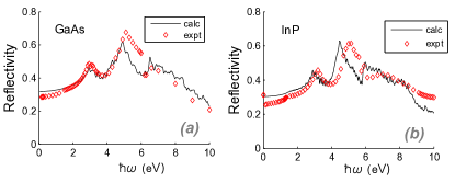
where is a scaling constant which is determined as follows. First the dielectric functions for all the ZB phase semiconductors are evaluated using empirical pseudopotential wave functions. The constant is then adjusted so that the calculated for ZB matches experimental values obtained from Ref. Madelung, 2004. By empirically fitting to this method results in good agreement between theory and experiment for frequencies . As an example, we show a comparison between the calculated and measured reflectivity spectra at normal incidence for cubic GaAs and InP in Fig. 1. The measured dielectric functions for GaAs and InP were obtained from Ref. Palik, 1998.
For the WZ calculations, and obtained using Eq. II are multiplied by the same scaling constant, . We expect this method to yield good results for the WZ semiconductors since both polytypes consist of the same atomic species, so the corrections to account for missing core states will be the same.
III Results and Discussion
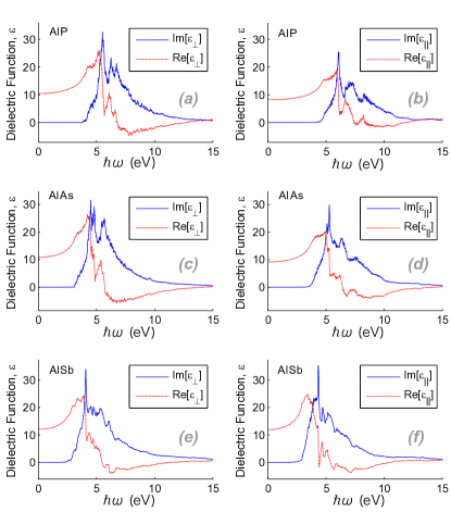
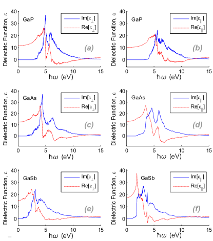
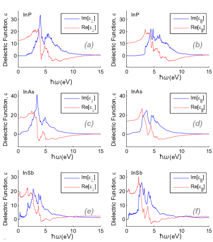
The calculated for light polarized parallel and perpendicular to the -axis are listed in table.1. The values listed in the table show that generally, materials with heavier elements have larger static dielectric constants. We also see that in the case of GaAs, GaSb and InSb, whereas for AlP, AlAs, GaP InP, and InAs.
| Material | ||
|---|---|---|
| AlP | 10.464 | 8.232 |
| AlAs | 10.853 | 9.165 |
| AlSb | 12.056 | 11.933 |
| GaP | 11.708 | 10.223 |
| GaAs | 12.481 | 13.066 |
| GaSb | 15.215 | 17.621 |
| InP | 12.812 | 10.435 |
| InAs | 16.782 | 13.610 |
| InSb | 16.952 | 19.379 |
| for | for | for | for | ||||||||||||||||||
|---|---|---|---|---|---|---|---|---|---|---|---|---|---|---|---|---|---|---|---|---|---|
| material | (eV) | ||||||||||||||||||||
| AlP | 4 | 130.1 | 5.639 | 6.064 | 4.927 | -0.7225 | 1.062 | 2.075 | -9.482 | 4.059 | 0.2963 | 137.3 | 6.702 | 7.095 | 5.742 | 8.292 | 0.3597 | 2.045 | -4.889 | 4.374 | 0.2395 |
| AlAs | 3.5 | 98.66 | 5.281 | 7.39 | 3.945 | -0.7937 | 6.019 | 1.775 | -1.505 | 3.525 | 0.3752 | 111 | 5.818 | 5.958 | 4.774 | 1.94 | 0.3517 | 1.775 | -1.349 | 3.564 | 0.3594 |
| AlSb | 3.5 | 173.3 | 24.43 | 1048 | 4.006 | -0.9518 | 29.01 | 1.775 | -2.341 | 3.574 | 0.6396 | 123.5 | 6.17 | 8.954 | 4.006 | -0.7481 | 10.49 | 1.775 | -1.476 | 3.605 | 0.4174 |
| GaP | 4 | 214.4 | 13.87 | 104.8 | 4.715 | -1.357 | 18.66 | 2.045 | -2.168 | 4.011 | 0.6816 | 142.9 | 6.11 | 6.582 | 5.157 | -3.88 | 5.39 | 2.045 | -8.046 | 4.257 | 0.3438 |
| GaAs | 2.5 | 35.06 | 2.279 | 1.548 | 2.781 | 0.3765 | 6.239 | 1.295 | -0.0002109 | 2.064 | 0.9754 | 160.6 | 22.74 | 666.6 | 3.696 | 1.721 | 2.93 | 1.295 | -5.471 | 2.515 | 0.6727 |
| GaSb | 1.5 | 21.1 | 1.652 | 1.416 | 1.825 | 0.3051 | 109.5 | 0.7851 | -3.005 | 2.201 | 0.0881 | 46.47 | 2.319 | 2.244 | 2.424 | 0.0002 | 0.4912 | 0.7852 | -0.0001 | 1.488 | 0.6783 |
| InP | 2.5 | 43.84 | 2.616 | 1.958 | 2.89 | 0.4301 | 14.99 | 1.295 | -4.324 | 2.962 | 1.289 | 74.09 | 3.942 | 3.117 | 4.005 | -9.183 | 1.076 | 1.295 | -6.656 | 2.502 | 0.8105 |
| InAs | 1 | 10.68 | 1.079 | 0.9922 | 1.269 | 0.2729 | 2.157 | 0.5467 | 7.456 | 1.042 | 0.7514 | 9.755 | 1.186 | 1.171 | 1.319 | -0.3299 | 1.332 | 0.5424 | -5.915 | 1.17 | 0.7103 |
| InSb | 0.5 | 2.54 | 0.5128 | 0.429 | 0.6435 | -0.1199 | 0.3746 | 0.2754 | -0.0012 | 0.414 | 0.2541 | 3.401 | 0.5733 | 0.4854 | 0.6665 | -0.1552 | 0.7352 | 0.2748 | -0.0003 | 0.5696 | 0.2978 |
For WZ materials, with the inclusion of spin-orbit interactions, all zone center states belong to either , or representations (all in double group notation). The zone center conduction band minima have either or symmetry and the valance band states are the heavy-hole, light-hole and a split-off-hole. The interband transitions for WZ are dictated by the polarization dependent optical selection rules Birman (1959a); Streitwolf (1969). For light polarized parallel to the -axis (), only transitions between states with the same symmetry are allowed, i.e. , and . For light polarized perpendicular to the -axis(), the allowed transitions are , , and . Note, that the transition is forbidden for all polarizations.
The other high symmetry k-point transitions allowed for are , , , , and . For the allowed dipole transitions are , , and . All M and U valley transitions (i.e. and ) are allowed for all polarizations. For a comprehensive list of optical selection rules for WZ at various high symmetry points and along various directions, see Refs. Streitwolf, 1969 and Mojumder, 1982 .
The zone center transition energies for the first thirteen states and their respective irreducible representations are listed in Ref.De and Pryor, 2010. Our band structure calculations show that the indirect gap ZB semiconductors (AlP, AlAs, AlSb and GaP) have direct band gaps in WZ phase De and Pryor (2010) with conduction band minima. These materials will be partially optically active, with transitions from the heavy-hole bands allowed for , making them potentially technologically important. The other semiconductors with conduction band minima in WZ phase are GaAs and GaSb. The Indium containing WZ semiconductors all have direct band gaps with conduction band minima and are optically active for all polarizations of the electric field.
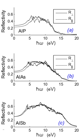
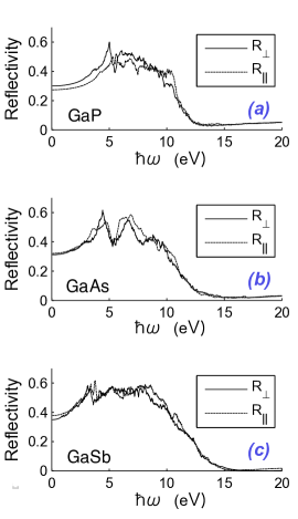
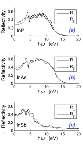
The calculated and for light polarized parallel and perpendicular to the -axis for the nine III-V semiconductors of interest are shown in Figs. 2-4 The corresponding reflectivity spectra for both polarizations is shown in Figs. 5-4. The reflectivity spectra for the different WZ crystals are distinct and depend on the details of its electronic band structure. For the WZ semiconductors, the most prominent features are typically seen up to about . As expected, all the WZ phase semiconductors exhibit optical anisotropy, the degree of which varies with the semiconductor. The reflectivity spectra for the two different polarizations shows several peaks which originate from interband transitions along various high symmetry points.
In order to illustrate the the dielectric function’s variations about the fundamental absorption edge (FAE), we fit the numerically calculated and (in the vicinity of their respective band gaps) to the Lorentz oscillator model. The real and imaginary parts of which are
| (12) |
| (13) |
where, and were used as fitting parameters and are listed in table 2. Note that the real and imaginary parts of the dielectric functions were separately fit to Eq.12 and Eq.13.
It is seen, that in general, is greater than . Based on optical selection rules, this can be explained by the fact that for a transition between the heavy-hole (HH) and the (or ) conduction band (CB) is allowed. Hence the FAE is at the bandgap (). For the allowed transition with the lowest energy will be between the light-hole (LH) and . As a result for , InP, InAs and InSb, the FAE will be at where is the energy difference between the heavy-hole and light-hole. In general, Indium containing compounds have prominent features in the reflectivity spectra near the FAE as a number of valance band to conduction band transitions are allowed. In all others (AlP, AlAs, AlSb, GaP, GaAs and GaSb) no noticeable sharp features are seen in the vicinity of the FAE since they all have CBs and the optical selection rules forbid transitions from the LH and the split-off hole for all polarizations and from the HH for .
The spin-orbit coupling can alter the ordering of the valence band states in different WZ semiconductors. In our calculations, the valance band states in all materials except InSb have normal ordering (i.e , , Birman (1959a); Thomas and Hopfield (1959)). The ordering of the valence band states in InSb is complicated by the very large spin-orbit splitting which forces the split-off hole bellow the next state, resulting in the unusual , , , valence band ordering. Attempts to optically measure the spin-orbit splitting energy in WZ type InSb could be complicated by this.
IV Summary
In summary we have calculated the optical properties of AlP, AlAs, AlSb, GaP, GaAs, GaSb, InP, InAs and InSb in WZ phase using empirical pseudopotentials. Their complex dielectric function was evaluated as a function of incident photon energy up to for light polarized parallel and perpendicular to the -axis. The dielectric functions were calculated in the dipole approximation by evaluating the optical momentum matrix elements using empirical pseudopotential wave functions (from Ref.De and Pryor, 2010) on a grid of about special k-points. Corrections to the pseudo-momentum-matrix elements to account for the missing core states are introduced via a scaling factor, which is determined from the ratio of the calculated to measured static dielectric function for the corresponding zincblende polytypes. The reflectivity spectra for all nine WZ semiconductors was also calculated for both polarizations and was seen to exhibit optical anisotropy as well. We have also calculated the static frequency dielectric constants.
References
- Cardona and Harbeke (1965) M. Cardona and G. Harbeke, Phys. Rev. 137, A1467 (1965).
- Reynolds et al. (1965) D. C. Reynolds, C. W. Litton, and T. C. Collins, Phys. Rev. 140, A1726 (1965).
- Xu and Ching (1993) Y.-N. Xu and W. Y. Ching, Phys. Rev. B 48, 4335 (1993).
- Ninomiya and Adachi (1995) S. Ninomiya and S. Adachi, Journal of Applied Physics 78, 1183 (1995).
- Kawashima et al. (1997) T. Kawashima, H. Yoshikawa, S. Adachi, S. Fuke, and K. Ohtsuka, Journal of Applied Physics 82, 3528 (1997).
- Alemu et al. (1998) A. Alemu, B. Gil, M. Julier, and S. Nakamura, Phys. Rev. B 57, 3761 (1998).
- Birman (1959a) J. L. Birman, Phys. Rev. 114, 1490 (1959a).
- Streitwolf (1969) A. H. W. Streitwolf, Physica Status Solidi (b) 33, 225 (1969).
- Wang et al. (2001) J. Wang, M. S. Gudiksen, X. Duan, Y. Cui, and C. M. Lieber, Science 293, 1455 (2001).
- Mattila et al. (2006) M. Mattila, T. Hakkarainen, M. Mulot, and H. Lipsanen, Nanotechnology 17, 1580 (2006).
- Mattila et al. (2007) M. Mattila, T. Hakkarainen, H. Lipsanen, H. Jiang, and E. I. Kauppinen, Appl. Phys. Lett. 90, 033101 (2007).
- Mishra et al. (2007) A. Mishra, L. V. Titova, T. B. Hoang, H. E. Jackson, L. M. Smith, J. M. Yarrison-Rice, Y. Kim, H. J. Joyce, Q. Gao, H. H. Tan, et al., Appl. Phys. Lett. 91, 263104 (pages 3) (2007).
- Lan et al. (2008) A. Lan, J. Giblin, V. Protasenko, and M. Kuno, Applied Physics Letters 92, 183110 (pages 3) (2008).
- Kobayashi et al. (2008) Y. Kobayashi, M. Fukui, J. Motohisa, and T. Fukui, Physica E: Low-dimensional Systems and Nanostructures 40, 2204 (2008), ISSN 1386-9477, 13th International Conference on Modulated Semiconductor Structures.
- Novikov et al. (2010) B. V. Novikov, S. Y. Serov, N. G. Filosofov, I. V. Shtrom, V. G. Talalaev, O. F. Vyvenko, E. V. Ubyivovk, Y. B. Samsonenko, A. D. Bouravleuv, I. P. Soshnikov, et al., physica status solidi (RRL) Rapid Research Letters 4, 175 (2010).
- Sercel and Vahala (1990) P. Sercel and K. Vahala, Physical Review B 42, 3690 (1990).
- Persson and Xu (2004) M. P. Persson and H. Q. Xu, Phys. Rev. B 70, 161310 (2004).
- De and Pryor (2010) A. De and C. E. Pryor, Phys. Rev. B 81, 155210 (2010).
- Birman (1959b) J. L. Birman, Phys. Rev. Lett. 2, 157 (1959b).
- Joannopoulos and Cohen (1973) J. D. Joannopoulos and M. L. Cohen, Phys. Rev. B 8, 2733 (1973).
- Pugh et al. (1999) S. K. Pugh, D. J. Dugdale, S. Brand, and R. A. Abram, J. Appl. Phys. 86, 3768 (1999).
- Pennington and Goldsman (2001) G. Pennington and N. Goldsman, Phys. Rev. B 64, 045104 (2001).
- Fritsch et al. (2006) D. Fritsch, H. Schmidt, and M. Grundmann, Appl. Phys. Lett. 88, 134104 (2006).
- Cohen and Chelikowsky (1988) M. Cohen and J. R. Chelikowsky, Electronic Structure and Optical Properties of Semiconductors (Springer, Berlin, 1988).
- Kageshima and Shiraishi (1997) H. Kageshima and K. Shiraishi, Phys. Rev. B 56, 14985 (1997).
- Adolph et al. (2001) B. Adolph, J. Furthmüller, and F. Bechstedt, Phys. Rev. B 63, 125108 (2001).
- Pickard and Mauri (2001) C. J. Pickard and F. Mauri, Phys. Rev. B 63, 245101 (2001).
- Monachesi et al. (2001) P. Monachesi, A. Marini, G. O. andM. Palummo, and R. D. Sole, physica status solidi (a) 184, 101 (2001).
- L. P. Mosteller and Wooten (1968) J. L. P. Mosteller and F. Wooten, J. Opt. Soc. Am. 58, 511 (1968).
- Brehat and Wyncke (1991) F. Brehat and B. Wyncke, Journal of Physics D: Applied Physics 24, 2055 (1991).
- Wang and Klein (1981) C. S. Wang and B. M. Klein, Phys. Rev. B 24, 3417 (1981).
- Monkhorst and Pack (1976) H. J. Monkhorst and J. D. Pack, Phys. Rev. B 13, 5188 (1976).
- Read and Needs (1991) A. J. Read and R. J. Needs, Phys. Rev. B 44, 13071 (1991).
- Adolph et al. (1996) B. Adolph, V. I. Gavrilenko, K. Tenelsen, F. Bechstedt, and R. Del Sole, Phys. Rev. B 53, 9797 (1996).
- Madelung (2004) O. Madelung, ed., Semiconductors Data Handbook (Springer-Verlag, Berlin Heidelberg New York, 2004), ed.
- Palik (1998) E. D. Palik, ed., Handbook of optical constants of solids (Academic Press, London, 1998).
- Mojumder (1982) M. A. Mojumder, Solid State Communications 43, 13 (1982), ISSN 0038-1098.
- Thomas and Hopfield (1959) D. G. Thomas and J. J. Hopfield, Phys. Rev. 116, 573 (1959).