Microwave inductance of thin metal strips
Abstract
We have measured the frequency-dependent, complex impedance of thin metal strips in a broad range of microwave frequencies (45 MHz to 20 GHz). The spectra are in good agreement with theoretical predictions of an RCL model. The resistance, inductance, and capacitance, which govern the microwave response, depend on the strip width and thickness as well as on the strip and substrate materials. While the strip resistance scales inversely with the cross section, the inductance depends on the width of the strip, but not on the thickness (in the limit of small thickness).
To properly design and thoroughly analyze the inductance of electrical circuitry at high frequencies is essential for a wide range of commercial applications as well as in fundamental research. The most basic element here is a conducting wire, which might have the shape of a spiral coilyue2000 ; cao2003 or act as an interconnect.tunnell2008 ; li2009 The inductance of a simple geometry might be calculated easily,grover1946 ; terman1943 but these calculations fail for more complex structures. For GHZ frequencies, finding the appropriate model for a realistic device can be challenging due to features like skin effect, coupling between different conductors, self inductance of thin strips, and the possible influence of a substrate. These effects become more complex if the material has a frequency-dependent conductivity. It is therefore necessary to distinguish between effects caused by geometry and by material properties. To test the validity of a possible model, one should compare it to measured data. In this work we concentrate on the simplest possible inductive structure, a straight metallic wire. This is in contrast to recent studies which address certain specific, device-relevant inductive structures.yue2000 ; cao2003 ; tunnell2008 ; li2009 We study a large variety of thin metallic strips, and we present microwave measurements covering an extremely broad frequency range up to 20 GHz.
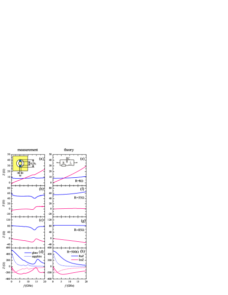
Similar to leads on circuit boards or in chips, our wires are created by deposition of a thin metallic film on top of a dielectric, i.e. the strips have thickness , width , and length , with . We will describe this ‘device’ with the lumped elements shown in the inset of Fig. 1(e): the wire has a resistance in series with its inductance , and in parallel the capacitance due to the dielectric substrate has to be taken into account. The complex impedance of this circuit as a function of angular frequency is:
| (1) |
We will consider frequencies as high as 20 GHz, but even then the skin depth will be much larger than , and therefore and will only depend on the wire geometry and material (and not on frequency). For such a strip, the geometric or Faraday inductance is given by yue2000 ; Greenhouse1974
| (2) |
where is the inductance in nH, and the length , the width , and the thickness are in mm.
The dimension of the strip that affects the inductance most strongly is the length . The width has a much weaker influence, and the strip thickness can be neglected completely for our limit (). This is in contrast to the resistance , which is inversely proportional to the strip cross section and depends on the material properties via its resistivity . The frequency dependence of the impedance , Eq. (2), can differ drastically, depending on the values of , , and . For certain combinations of and , this also holds if these two quantities are kept constant and only is varied. In Fig. 1 we demonstrate this by combining experimental and theoretical data.
In the experiment, we compare numerous samples. Each consists of a metallic strip, prepared by thermal evaporation of nichrome (NiCr), lead (Pb), or aluminum (Al) and deposition onto a glass or sapphire substrate through a shadow mask. The width and thickness of the different strips vary over substantial ranges. The microwave measurements are performed at room temperature with a Corbino spectrometerscheffler2005a that is suitable for this particular geometry,scheffler2007 as shown in the inset of Fig. 1(a): concentric gold contacts in Corbino geometry (inner diameter , outer diameter ) are deposited on top of the strip. We then measure the complex reflection coefficient, which directly reveals the sample impedance.scheffler2005a ; stutzman2000 We have performed a full three standard calibration using as references an Al plate (short), a NiCr thin film (load), and a Teflon cylinder (open). Due to the particular geometry, the sample impedance is that of two strips [with length , width , and thickness ] in parallel.

In Figs. 1(a)-(d) we present experimental impedance spectra spanning the very broad frequency range = 45 MHz to = 20 GHz. =1.75 mm and =0.8 mm are kept constant for all measurements. For these data, our choices of , , and strip material only weakly affect and of the sample, but drastically change . Therefore, we compare the experimental data to theoretical impedance spectra, Figs. 1(e)-(h), where we keep nH and fF constant, but vary . In general, we can describe the experimental data very closely with the simple RCL model, except for an impedance increase toward the lowest frequencies [in Figs. 1(a), (b), due to capacitive contributions to the contact impedance]steinberg2008 and a resonance feature around 12-15 GHz for glass substrates and 8-10 GHz for sapphire substrates (due to a volume mode governed by the dielectric substrate).scheffler2010 ; kitano2008
Tuning over a large range, we find rather different frequency dependences, depending on the ratio : For [Figs. 1(a), (e)], Re() is almost constant whereas Im() roughly increases linearly with frequency. For slightly smaller than [Figs. 1(b), (f)], Im() almost vanishes whereas Re() is almost constant. For slightly larger , now exceeding , Re() develops a downturn toward higher frequencies, and Im() is negative, decreasing linearly with frequency. For the extreme case , Re() starts at Re((=0))= and decreases strongly with increasing frequency, roughly as 1/, whereas Im()0 first decreases linearly with and then approaches zero from below as -1/; the minimum occurs for =1/(2). For this last case,scheffler2007 we additionally present data for a slightly thicker NiCr strip deposited on a substrate of sapphire (instead of glass). Due to the larger dielectric constant of sapphire, the capacitance between inner and outer Corbino contact increases and the characteristic frequency dependence in Figs. 1(d), (h) moves to lower frequencies.

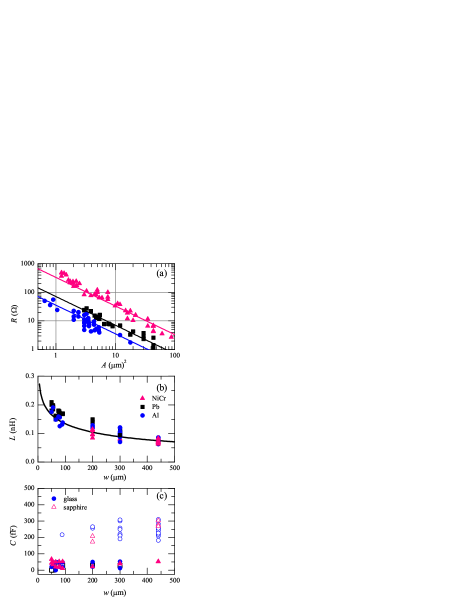
The real and imaginary parts of the measured impedance spectra were simultaneously fitted with Eq. (1) to obtain , , and for different strip geometries.CommentFit As evident from Fig. 1, the measured spectra and the model spectra agree quite well; thus , , and can be determined from these fits. The fitting error of these parameters vary depending on the particular regime of the impedance spectrum: while can always be determined reliably, has a large fitting error except for the large- case [Fig. 1(d)], where the pronounced frequency dependence is governed by . Similarly, can precisely be determined for small [Fig. 1(a)], but in addition also for those cases, where and both are large [like the sapphire case in Fig. 1(d)].
The results of these fits are shown in Fig. 2. The resistance of a strip is expected to depend on the dc resistivity of the strip material and the strip cross section . This is exactly what we see in Fig. 2(a): for each material (NiCr, Pb, and Al), depends inversely on (as indicated by the straight line, which is a fit with as fitting parameter: cm, cm, cm. The imprecise determination of the film thickness of the aluminum samples leads to data the data scattering. More relevant for our interest is the inductance [Fig. 2(b)] that we obtain from the fits: according to Eq. (2) we expect that for our samples ( constant; ) the inductance will only depend on , and this is what we find. Independent of strip material and thickness, the width dependence of follows Eq. (2) as indicated by the full line in Fig. 2(b). For the capacitance as the third fitting parameter, on the other hand, the dependence on should only be weak,scheffler2007 but it should depend strongly on the dielectric constant of the substrate material. This is seen in Fig. 2(c); the devices on sapphire substrates (open symbols) have a much higher capacitance than those on glass substrates (closed symbols), and within each substrate material there is, within the data scattering, no width dependence. The scattering of the data is mostly due to the inaccurate determination of for inductance dominated samples.
We have investigated the microwave impedance of thin metallic strips and we could successfully describe their frequency dependence with an RCL model. In particular, we have shown how the geometric inductance contributes to the overall impedance and how it depends on the strip width. This is not only relevant for the design of microwave devices, but also for fundamental research. For example, for several materials of current interest, such as superconductors,steinberg2008 ; booth1996 interacting electron systems,scheffler2010 ; scheffler2005b or two-dimensional electron gases,burke2000 the intrinsic conductivity is frequency dependent even for frequencies as low as a few GHz. When these materials are studied using microwaves, the imaginary part of the complex conductivity shows up as an inductive contribution. In this case, one has to know the geometric inductance, as presented in this Paper, before one can determine the intrinsic inductance stemming from the material.
We thank Gabriele Untereiner for the sample fabrication and René Ramsperger and Serife Kilic for some of the microwave measurements. We acknowledge financial support by the DFG and SFB/TRR21.
References
- (1) C. P. Yue and S. S. Wong, IEEE Trans. Electron Devices 47, 560 (2000).
- (2) Y. Cao et al., IEEE J. Solid-State Circuits 38, 419 (2003).
- (3) A. Tunnell, V. Ballarotto, D. Hines, and E. Williams Appl. Phys. Lett. 93, 193113 (2008).
- (4) H. Li and K. Banerjee, IEEE Trans. on Electron Devices 56, 2202 (2009).
- (5) W. Frederick, Grover, Inductance Calculations (Dover, Mineola Ny, 1946).
- (6) F. E. Terman, Radio Engineering Handbook (McGraw-Hill, New York, 1943).
- (7) H. M. Greenhouse, IEEE Trans. Parts, Hybrids, Packag. 10, 101 (1974).
- (8) M. Scheffler and M. Dressel, Rev. Sci. Instrum. 76, 074702 (2005).
- (9) M. Scheffler, S. Kilic, and M. Dressel, Rev. Sci. Instrum. 78, 086106 (2007).
- (10) M. L. Stutzman, M.Lee, and R. F. Bradley, Rev. Sci. Instr. 71, 4596 (2000).
- (11) K. Steinberg, M. Scheffler, and M. Dressel, Phys. Rev. B 77, 214517 (2008).
- (12) M. Scheffler, M. Dressel, and M. Jourdan, Eur. Phys. J. B 74, 331 (2010).
- (13) H. Kitano, T. Ohashi, and A. Maeda, Rev. Sci. Instrum. 79, 074701 (2008).
- (14) To exclude the influence of the oxide layer for Al and Pb strips steinberg2008 their data were fitted above 1 GHz.
- (15) J. C. Booth, D. H. Wu, S. B. Qadri, E. F. Skelton, M. S. Osofsky, Alberto Piqué, and Steven M. Anlage, Phys. Rev. Lett. 77, 4438 (1996).
- (16) M. Scheffler, M. Dressel, M. Jourdan, and H. Adrian, Nature 438, 1135 (2005).
- (17) P. J. Burke, I. B. Spielman, J. P. Eisenstein, L. N. Pfeiffer, and K. W. West, Appl. Phys. Lett. 76, 745 (2000).