Further author information: (Send correspondence to H. Tajima)
H. Tajima: E-mail: tajima@stanford.edu, Telephone: 1 650 926 3035
Soft Gamma-ray Detector for the ASTRO-H Mission
Abstract
ASTRO-H is the next generation JAXA X-ray satellite, intended to carry instruments with broad energy coverage and exquisite energy resolution. The Soft Gamma-ray Detector (SGD) is one of ASTRO-H instruments and will feature wide energy band (40–600 keV) at a background level 10 times better than the current instruments on orbit. SGD is complimentary to ASTRO-H’s Hard X-ray Imager covering the energy range of 5–80 keV. The SGD achieves low background by combining a Compton camera scheme with a narrow field-of-view active shield where Compton kinematics is utilized to reject backgrounds. The Compton camera in the SGD is realized as a hybrid semiconductor detector system which consists of silicon and CdTe (cadmium telluride) sensors. Good energy resolution is afforded by semiconductor sensors, and it results in good background rejection capability due to better constraints on Compton kinematics. Utilization of Compton kinematics also makes the SGD sensitive to the gamma-ray polarization, opening up a new window to study properties of gamma-ray emission processes. The ASTRO-H mission is approved by ISAS/JAXA to proceed to a detailed design phase with an expected launch in 2014. In this paper, we present science drivers and concept of the SGD instrument followed by detailed description of the instrument and expected performance.
keywords:
gamma-ray, Compton telescope, Polarimeter, Silicon Detector, CdTe, semiconductor detector1 INTRODUCTION
ASTRO-H, the new Japanese X-ray Astronomy Satellite[1, 2] following the currently-operational Suzaku mission, aims to fulfill the following scientific goals:
-
•
Revealing the large-scale structure of the universe and its evolution.
-
•
Understanding the extreme conditions of the universe.
-
•
Exploring the diverse phenomena of the non-thermal universe.
-
•
Elucidating dark matter and dark energy.
In order to fulfill the above objectives, the ASTRO-H mission hosts the following instruments: high energy-resolution soft X-ray spectrometer covering the 0.3–10 keV band, consisting of thin-foil X-ray optics (SXT, Soft X-ray Telescope) and a microcalorimeter array (SXS, Soft X-ray Spectrometer); soft X-ray imaging spectrometer sensitive over the 0.5–12 keV band, consisting of an SXT focussing X-rays onto CCD sensors (SXI, Soft X-ray Imager); hard X-ray imaging spectrometer, sensitive over the 3–80 keV band, consisting of multi-layer-coated, focusing hard X-ray mirrors (HXT, Hard X-ray Telescope) and silicon (Si) and cadmium telluride (CdTe) cross-strip detectors (HXI, Hard X-ray Imager)[3, 4, 5, 6, 7]; and soft gamma-ray spectrometer covering the 40–600 keV band, utilizing the semiconductor Compton camera with narrow field of view (SGD, Soft Gamma-ray Detector)[3, 4, 5, 6, 8]. The SXT-SXS and SGD systems will be developed by international collaboration led by the Japanese, US and European institutions.
The SXS will use a element microcalorimeter array. The energy resolution is expected to be better than 7 eV. In conjunction with the 6 m focal-length SXT, the field of view and the effective area will be, respectively, about 3 arc minutes and about 210 cm2. The SXT-SXS system will provide accurate measurements of the temperature and the turbulence/macroscopic motions of intra-cluster medium in distant clusters of galaxies up to redshift of about 1, allowing studies of the formation history of the large scale structure of the universe, which in turn will eventually constrain the evolution of the dark energy.
The focal length of the HXT will be 12 m and the effective area will be larger than 200 cm2 at 50 keV. The HXI detector utilizes four layers of double-sided Si strip detectors overlaid on a double-sided CdTe strip detector with a BGO (Bi4Ge3O12) active shield. The extremely low background of the HXT-HXI system will improve the sensitivity in 20–80 keV range by almost two orders of magnitude as compared to conventional non-imaging detectors in this energy band. The search for highly absorbed active galactic nuclei and understanding their evolution is one of main science topics of the HXT-HXI.
The SGD also utilizes semiconductor detectors using Si and CdTe pixel sensors with good energy resolution (2 keV) for the Compton camera, which was made possible by recent progress on the development of high quality CdTe sensors[9, 10, 11, 12]. The BGO active shield provides a low background environment by rejecting the majority of external backgrounds. Internal backgrounds are rejected based on the inconsistency between the constraint on the incident angle of gamma rays from Compton kinematics and that from the narrow FOV (field of view) of the collimator. This additional background rejection by Compton kinematics will improve the sensitivity by an order of magnitude in the 40–600 keV band compared with the currently operating space-based instruments. Science objectives of the SGD include studies of particle acceleration in various sources via measurement of non-thermal emission and the high-energy cutoff, origin of the emission in the GeV gamma-ray emission though the observation of non-thermal bremsstrahlung signatures expected in the SGD band, and searches for origin of 511 keV emission from electron-positron annihilation. In addition, the SGD will be sensitive to the polarization in the 50–200 keV band from a number of accreting Galactic black hole and neutron star binaries, and for active galactic nuclei in flaring states.
The ASTRO-H mission has just completed the preliminary design phase, aimed at verifying that the design of the system/subsystems/components will meet the mission requirements with sufficient reliability to accomplish the mission objectives, and to assure that system/subsystems/components designs are feasible in terms of technology and schedule via design analysis, fabrication and tests of bread board models. The expected launch date is in 2014.
2 Science Requirements and Drivers
The mission-level science objectives described above require the SGD to provide spectroscopy up to 600 keV for over 10 super-massive black holes with fluxes equivalent to 1/1000 of the Crab Nebula (as measured over the 2–10 keV band, assuming the spectrum to be a power-law with spectral index of 1.7). This mission-level science requirement defines the following instrument-level requirements for the SGD:
-
•
Effective area for the detector must be greater than 20 cm2 at 100 keV to obtain sufficient number of photon in a reasonable observation time (typically 100 ks);
-
•
Field of view must be 0.6∘ at 150 keV or less to minimize source confusion;
-
•
Energy resolution must be better than 2 keV to identify nuclear lines from activation backgrounds.
The SGD instrument with capabilities defined above will determine the non-thermal emission processes for a large range of celestial sources (via the measurement of broad-band spectral shape and and high-energy cutoff), with the goal of studying particle acceleration in GeV band. With some sources, parameters of non-thermal bremsstrahlung processes will be determined; and finally, SGD will enable the identification of the origin of 511 keV emission line, arising from electron-positron annihilation.
Measurements of spectra up to 600 keV for more than 10 AGNs (Active Galactic Nuclei) will enable a probe of existence of spectral breaks above 100 keV. Measurements of such spectral breaks will play a crucial role in solving the question on the origin of the soft gamma-ray emissions in AGN (whether the emission arises from the accretion disk or relativistic electrons in the jet). The detailed spectral measurements are expected to contribute to understanding of the soft gamma-ray emission in more than 10 X-ray pulsars and magnetars.
The SGD is also expected to be able to measure the spectrum of supernova remnants (with the prime example of Cas A), to determine whether it is indeed dominated by non-thermal bremsstrahlung, as expected on theoretical grounds. The soft gamma-ray flux measured by the SGD can determine the magnetic field of Cas A by combining the SGD data with those from other wavelength: this is essential when estimating the fluxes and spectra of electrons and protons accelerated in Cas A.
Perhaps the most unique SGD parameter is that Compton kinematics utilized in the SGD yield good sensitivity to the polarization in the 50–200 keV band from several Galactic black holes and neutron stars, and some AGNs in flare states. Detection of the gamma-ray polarization from these sources will bring new probes into the gamma-ray emission mechanism. Moreover, the detection of X-ray / soft gamma-ray polarization from sources at the cosmological distance will place stringent constraints on the violation of Lorentz invariance, which has a profound impact on the fundamental physics. Since X-ray polarization is largely unexplored, discovery potential is very high.
In summary, the SGD is expected to provide essential data towards studies of the origin of CXB (Cosmic X-ray background), particle acceleration in SNR, origin of the hard X-ray emission from the vicinity of accreting black holes such as X-ray binaries, the Galactic center, and AGN, and non-thermal emission from galaxy clusters.
3 Instrument Concept
The SGD concept originates from Hard X-ray Detector (HXD)[13] onboard Suzaku satellite. The HXD consists of Si photodiodes and GSO scintillators with BGO active shield and copper passive collimator, and achieved the best sensitivities in the hard X-ray band. The SGD replaces the Si photodiodes and GSO scintillators in HXD with the Compton camera, which provides additional background rejection capabilities based on Compton kinematics. Figure 1 (a) shows a conceptual drawing of a SGD unit. A BGO collimator defines 10∘ FOV of the telescope for high energy photons while a fine collimator restricts the FOV to 0.6∘ for low energy photons (150 keV), which is essential to minimize the CXB (cosmic X-ray backgrounds) and source confusions. Scintillation light from the BGO crystals is detected by avalanche photo-diodes (APDs) allowing a compact design compared with phototubes.
The hybrid design of the Compton camera module incorporates both pixelated Si and CdTe detectors. The Si sensors are used as the scatterer since Compton scattering is the dominant process in Si above 50 keV compared with 300 keV for CdTe. The Si sensors also yield better constraints on the Compton kinematics because of smaller effect from the finite momentum of the Compton-scattering electrons (Doppler broadening) than CdTe (approximately by a factor of two). The CdTe sensors are used as the absorber of the gamma ray following the Compton scattering in the Si sensors. Combination of two materials with low and high (atomic number) are also beneficial for lowering backgrounds since neutron scattering is suppressed in high-Z material and activation backgrounds are negligible in low- material. Note that neutron and activation backgrounds are the dominant background contributions in the SGD.
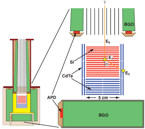 |
We require each SGD event to interact twice in the Compton camera, once by Compton scattering in a Si sensor, and then by photo-absorption in a CdTe sensor. Once the locations and energies of the two interactions are measured, as shown in Figure 1, the Compton kinematics can be calculated by the direction of the incident photon with the formula,
| (1) |
where is the polar angle of the Compton scattering, and and are the energy deposited in each photon interaction. The high energy resolution of the Si and CdTe devices is essential in reducing the uncertainty of . The angular resolution is limited to 8∘ at 100 keV due to the Doppler broadening and 3∘ at 600 keV due to pixel size of the semiconductor sensor. We require that the incident photon angle inferred from the Compton kinematics is consistent with the FOV, which dramatically reduces dominant background sources such as radio-activation of the detector materials and neutrons. Low background realized by the Compton kinematics is the key feature of SGD since the photon sensitivity of SGD is limited by the backgrounds, not the effective area.
As a natural consequence of the Compton approach used to decrease backgrounds, SGD is quite sensitive to X/gamma-ray polarization, thereby opening up a new window to study the geometry of the particle acceleration and emission regions, and the magnetic field in compact objects and astrophysical jets. The Compton scattering cross section depends on the azimuth Compton scattering angle with respect to the incident polarization vector as;
| (2) |
where and are the azimuth and polar Compton scattering angles, and and are incident and scattered photon energies. It shows that the modulation is largest at , i.e. perpendicular to the incident polarization vector.
4 Instrument Design
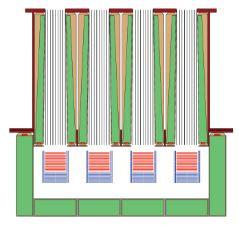
SGD consists of two identical set of a SGD-S, two SGD-AE, a SGD-DPU and a SGD-DE. SGD-S is a detector body that includes a array of identical Compton camera modules surround by BGO shield units and fine passive collimators as shown in Figure 2 (a). Two SGD-S are mounted on opposite sides of the spacecraft side panels to balance the weight load since it has a high mass (150 kg). It was determined that a array arrangement is preferred as it allows an increase of the BGO thickness for the same weight and can also keep a symmetry against 90∘ rotation which is important for polarization measurements. However, the current is employed to minimize the deformation of the spacecraft side panel. SGD cooling system is attached to the cold plate of the SGD-S housing. APD CSA (charge-sensitive amplifier) box and HV (high voltage) power supply are also attached to the SGD housing. SGD-AE is an electronics box that provides power management and housekeeping (HK) functions for Compton camera system and APD readout system. It also performs APD signal processing. SGD-DPU functions as a digital interface to the SGD-DE via SpaceWire network standard and also houses SGD-PSU (Power Supply Unit) inside. SGD-DE includes a microprocessor and performs data processing for event and HK data, and is connected to the satellite SpaceWire network. Topology of the SpaceWire network is designed to be redundant. Data can be routed via another DPU if one of DPU-DE or DE-router connections is broken. In addition, a spare DE shared by all instruments on the satellite is included in the payload: the data can be routed to the spare DE if one of the SGD-DEs malfunctions. Design details of each component are described below.
| (a) | (b) |
|---|---|
 |
|
4.1 Compton camera
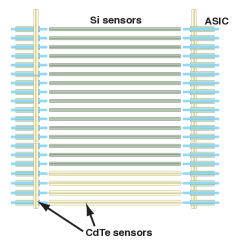
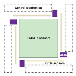
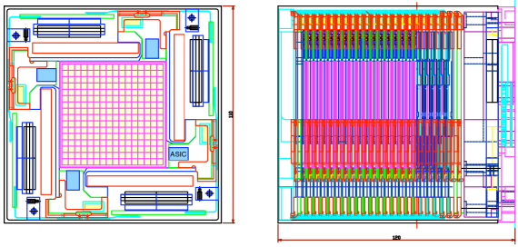
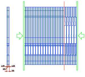
The Compton camera consists of 32 layers of Si sensors and 8 layers of CdTe sensors surrounded by 2 layers of CdTe sensors as shown in Figure 2 (b). The location of the CdTe sensors on the side is slightly displaced in the horizontal direction to allow placement of readout ASIC (Application Specific Integrated Circuit) at the corner of the sensor. This arrangement allows a placement of the CdTe sensor on the side very close to the stacked Si and CdTe sensors to maximize the coverage of the photons scattered by the Si sensors. In addition to sensor modules, the Compton camera holds an ACB (ASIC controller board) and four ADBs (ASIC driver boards). The ACB holds an FPGA (filed programmable gate array) that controls the ASIC and communicates with SpaceWire interface by a serial link. The ADB buffers control signals from the ACB and sends control signals to 52 ASICs, and also provides a current limiter to power the ASICs.
The mechanical structure of the Compton camera needs to hold all components described above within the size of cm3. This size constraint is imposed to minimize the size of BGO active shield since the BGO is the dominant contribution to the total weight of the SGD-S. Another important requirement for the mechanical structure is cooling of the sensors. The temperature of all sensors needs to be maintained to within 5∘C of the cold plate interface at the bottom of the Compton camera.
| (a) | (b) |
|---|---|
 |
 |
| (a) | (b) |
|---|---|
 |
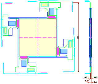 |
Figure 3 (a) shows the mechanical support structure of the Compton camera. The Compton Camera consists of a stack of Si and CdTe sensor trays as shown in Figure 3 (b), four CdTe sensor modules on the side, and also top and bottom frames to hold them together. The top and bottom frames are held together by four pillars with M3 screws. Each ADB is attached to the side CdTe sensor module and an ACB is attached to the bottom frame. The material of the camera structure must have the CTE (Coefficient for Thermal Expansion) close to those of Si and CdTe sensors (a few m/m/K). Currently, it is planned to employ PEEK (polyether ether ketone) loaded with carbon fibers for the trays and the top frame where a low- material is required, and titanium for the pillars and the bottom frame. Since the carbon fiber-filled PEEK is conductive, trays need to be conformal-coated by Parylene (commercial name of Xylylen polymers) to avoid shorting of the bias voltage for the sensors. Parylene can produce pinhole-free coating with high resistivity, uniform thickness and chemical tolerance.
| (a) | (b) |
 |
|
| (c) | |
 |
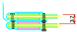 |
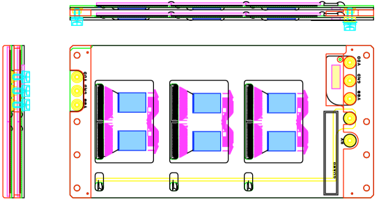
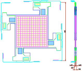
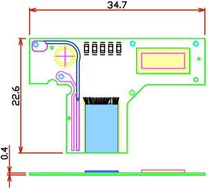
Each Si and CdTe sensor tray consists of Si or CdTe sensors and FEC (Front-End Card) mounted on both sides of the tray frame as shown in Figure 4. An ASIC is mounted on each FEC. Figure 5 shows the schematic drawings of a FEC, and a FPC that connects two FECs and an ADB. Two FECs are mounted at each corner of a tray and connected by an FPC as shown in Figure 5 (c).
Figure 6 shows drawings of side CdTe sensor module viewed from three directions. Two CdTe sensor boards are stacked together with PEEK spacers. A titanium frame will be attached on the back of this module to reinforce mechanical rigidity.
We have fabricated mechanical models of the Compton camera with slightly different materials (polycarbonate trays and aluminum pillars) and confirmed that those survive vibrations expected from the launch vehicle (HII-A). We plan to fabricate a mechanical model and a thermal model of the Compton camera with the final design and evaluate mechanical and thermal properties.
4.2 Si and CdTe sensors
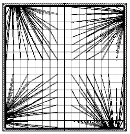
Si and CdTe sensors are pixellated to give two-dimensional coordinates with a pixel size of mm2 and a thickness of 0.6 mm for Si and 0.75 mm for CdTe. Pixel size is determined to minimize the number of pixels for lower power consumption while avoiding the pixel size to be the dominant contribution to the angular resolution of Compton kinematics. The thicknesses of Si and CdTe sensors are determined from constraints on the bias voltages required to operate the sensors at the best condition. In order to suppress the leakage current from the edge of the sensor, a guard ring is placed at the periphery of the sensor surrounding all the pixels. Each Si sensor has pixels providing cm2 active area. Signal of each pixel on the Si sensor is brought out to one of bonding pads at the corner of the sensor by a readout electrode laid out on top of the SiO2 insulation layer with a thickness of 1.5 m as shown in Figure 7 (a). For the readout purposes, the Si sensors are grouped into four quadrants of pixels.
A CdTe sensor has pixels providing cm2 active area since it is difficult to fabricate the CdTe sensor much larger than cm2. CdTe sensors are tiled in an array for each layer in the bottom and in an array for each layer on the side to obtain the required active area. In order to overcome small mobility and short lifetime of carriers in CdTe sensors, we employ a Schottky-barrier diode type CdTe sensor with Indium (In) anode and Platinum (Pt) cathode so that we can apply high bias voltage with low leakage current. Indium electrode functions as a common biasing electrode while Pt electrodes form pixels. Titanium is placed on the In electrode to reduce the resistance. Gold (Au) is placed on the Pt electrode to improve connection of In/Au stud bump bonding. Diode type CdTe sensors suffer degradation of energy resolution due to charge trapping over time which is called polarization. It is known that the polarization slows down at lower temperature and the effect of polarization can be reduced by applying higher bias voltage. For example, it was found that operation of this type of CdTe sensor for a week has little polarization effect at 5∘C and 1000 V/mm and this polarization effect can be recovered by turning off the bias voltage. Since the recovery process accelerates at a higher temperature, annealing the sensor to minimize the down time may be required.
CdTe sensors cannot have integrated readout electrodes above pixel electrodes on the device unlike Si sensors.
| (a) | (b) |
|---|---|
 |
 |
In addition, it is not possible to wire-bond on the electrodes of the CdTe sensor. In order to address those issues, we employ a separate fanout board to route signal from each pixel to the corner of the sensor where ASICs are placed. The fanout board is made of 0.3 mm thick ceramic (Al2O3) substrate that allows fine pitch between electrodes to match the input pitch of the ASIC (91 m). The CdTe sensor and the fanout board are bump-bonded via In/Au stud bump as shown in Figure 7 (b). ASIC and the fanout board are connected by wire bonding.
Table 1 summarizes specifications of Si and CdTe sensors.
| Description | Si | CdTe |
|---|---|---|
| Sensor active area | cm2 | cm2 |
| Pixel area | mm2 | mm2 |
| Number of pixels | ||
| Thickness of sensor | mm | mm |
| Thickness of depletion (active) layer | mm | mm |
| Thickness of inactive layer | mm | N/A |
| Bias voltage | 250 V | 1000 V |
| Leakage current per pixel @ ∘C | 50 pA | 50 pA |
| Leakage current per pixel @ ∘C | 4000 pA | 4000 pA |
| Width of readout electrode | 8 m | N/A |
| Thickness of insulation for readout electrodes | 1.5 m | N/A |
4.3 Application Specific Integrated Circuit
The main performance requirements for an ASIC are low noise ( keV FWHM), low power ( mW/channel) and fast readout time (s) to satisfy the 2% dead time for 100 Hz trigger rate. In order to satisfy those main requirements, an ASIC is developed based on the VIKING architecture[14, 15] which has been known for good noise performance and used in various space experiments like Swift, PAMELA and AGILE.
Figure 8 shows the circuit diagram for the ASIC developed for the SGD (and HXI). In the VIKING architecture ASIC, each channel consists of charge sensitive amplifier followed by two shapers. One shaper with a short shaping time is followed by a discriminator to form a trigger signal. The other shaper with a long shaping time is followed by a sample and hold circuit to hold the pulse height at the timing specified by an external hold signal.
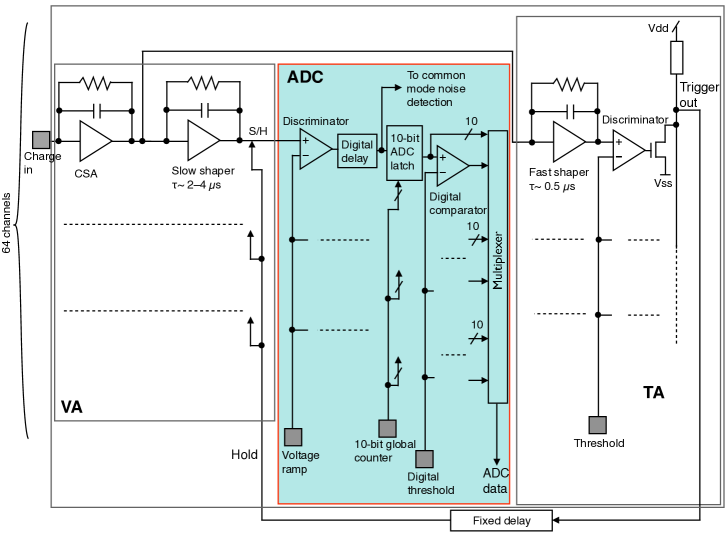
The hold signal is produced from the trigger signal with an appropriate delay.
Many important functionalities are integrated in the ASIC for the SGD in order to minimize additional components required to readout the signal as shown in the circuit diagram with a blue background region. As a result, we only need an FPGA, several digital drivers and receivers, and passive components (resistors and capacitors) to operate 208 ASICs in a Compton camera. The signals in all channels on the ASIC are converted to digital values in parallel with Wilkinson-type analog-to-digital converters (ADCs) where the time duration of voltage ramp to cross the sampled voltage is counted by a counter. The conversion time is less than 100 s using the external clock or less than 50 s using the internal clock. (The conversion time depends on the pulse height of the signal.) In order to minimize the readout time, the only channels that are read-out are those above a data threshold that can be digitally set for each channel independently from the trigger threshold. We usually observe common mode noise from this type of ASIC at the level of 1 keV (can be worse if power supplies and grounding are not appropriate). Common mode noise has to be subtracted to accurately apply the threshold for the zero suppression. Common mode noise level of each event is detected by taking an ADC value of the 32nd (a half of number of channel) pulse height, corresponding to a median value of all ADC values. With zero suppression, the readout time is s per ASIC when no data is readout and s when we readout channels. Without zero suppression, the readout time becomes s per ASIC.
The ASIC produces all necessary analog bias currents and voltages on the chip by internal DACs (Digital to Analog Converters) except for the main bias current which sets the scale of all bias currents: this is provided by an external circuit on the FEC. Each bit of the registers for all internal DACs and other functions consists of three flip-flops and a majority selector for tolerance against single event upset (SEU). If the majority selector detects any discrepancies among three flip-flops, it will set a SEU flag which will be readout as a part of output data. The ASIC is fabricated on a wafer with an epitaxial layer which will improve immunity against latch up. Table 2 summarizes specifications.
| Geometrical specifications | |
|---|---|
| Number of channels | 64 |
| Input pitch | 91 m |
| Thickness | 0.45 mm |
| Analog specifications | |
| Power consumption | 0.2 mW/channel |
| Fast shaper peaking time | 0.6 s |
| Slow shaper peaking time | 3 s |
| Noise performance | 180 (RMS) at 6 pF load |
| 1.5 keV (FWHM) for Si | |
| Threshold | 1500 at 6 pF load |
| 5.4 keV for Si | |
| Threshold range | 625 – 6250 |
| Threshold step | 208 |
| Dynamic range | 100,000 |
| 360 keV for Si | |
| Digital specifications | |
| ADC setup time | 5 s |
| ADC power consumption | 0.5–2 mW/channel |
| 5–20 W/channel at 100 Hz | |
| Data clock speed | 10 MHz |
| Conversion clock speed | 10 MHz (external clock) |
| 20 MHz (internal clock) | |
| Conversion time | 100 s (external clock) |
| 50 s (internal clock) | |
| Readout time (no data) | 0.5 s per ASIC |
| Readout time ( channels) | s per ASIC |
The data input and output circuits on the ASIC are designed to allow daisy-chaining of multiple ASICs. In one scheme, the data output of one ASIC can be connected to the input of another ASIC and the ASIC will pass the input data to the output via a shift register. This scheme is used to set register values. In another scheme, output of several ASICs can be connected to a single bus. The output is controlled by passing a token from ASIC to ASIC. Or, in the case of trigger signal, ASICs can issue trigger signals at any time since the output circuit is open-drain FET to allow multiple triggers on the same bus. In the Compton camera, 6 or 8 ASICs are daisy chained.
4.4 BGO active shield
The thick active shield made of BGO scintillator is employed to reduce in-orbit background of the SGD. The BGO crystal is heavy, and has a high stopping power, high transparency and ability to form larger crystal, while its light output is lower than NaI or CsI. Scintillating light from a BGO is detected via an APD.
In addition to providing veto signals for cosmic rays and gamma rays from outside of the FOV, the BGO shield is also used to reduce the number of SAA (South Atlantic Anomaly) protons since those protons are the main cause of the activation of sensor materials. The BGO shape is designed so that any trajectory that intersects with the Compton camera must go through at least 3 cm of BGO before it reaches the camera. In order to effectively detect cosmic rays and gamma rays that interact with the BGO, the detection threshold of the BGO readout system must be lower than 100 keV. This requirement imposes constraints on the BGO shape, reflector design, and the performance of the APD readout system. The BGO shield consists of 30 BGO crystals and their locations and shapes are indicated by green polygons in Figure 2 (a). The weight of each BGO module is 2–6 kg and total weight is 100 kg.
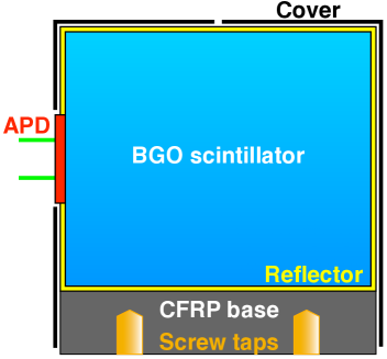
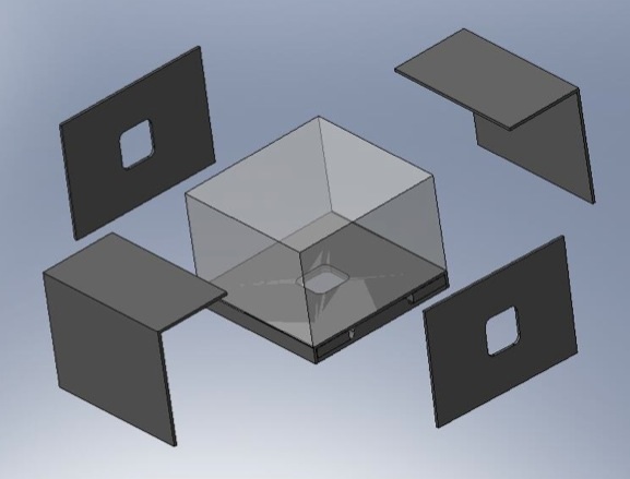
We employ a modular mechanical structure for the BGO shield where each BGO crystal is supported by a CFRP enclosure in order to make it easier to handle BGO modules. The BGO enclosure consists of a CFRP base that is glued to the BGO crystal via BaSO4-based reflector painted on the BGO, and CFRP covers as shown in Figure 9. The CFRP base screw holes to be used to attach them to the housing structure. BaSO4-based reflector is chosen for the mechanical strength that is required for the base bonding. The remaining sides of the BGO crystal is covered by both ESR (Enhanced Specular Reflector) and Gore-Tex sheet for better reflection properties.
4.5 Fine collimator
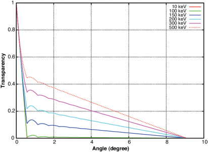
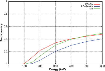
The BGO active shield has an opening of deg2, which is too large, resulting in CXB (cosmic X-ray backgrounds) higher than NXB (non X-ray backgrounds) and substantial source confusions within the FOV below 150 keV. Passive collimators called fine collimators (FCs) are installed in opening of the BGO active shield, to reduce the FOV to 33.3 arcmin (FWHM). Material and its thickness defines the maximum effective energy (100–150 keV) of the FC. Note that BGOs are thick enough to detect any gamma rays in the SGD energy band (600 keV). The default choice is 0.1 mm thick PCuSn (with a length of 324 mm), which yields the maximum effective energy of 100 keV as shown in Figure 10 (a). Collimator cell size is chosen at 3.2 mm yielding an aperture opening of 94%. In order to ensure a transparency better than 90%, the alignment of FC must be better than 10% of its FOV, 3 arcmin. Alignment mechanisms will be built into the mounting structure of the FC.
The FC material could be molybdenum (Mo) to obtain higher maximum effective energy, 150 keV as shown in Figure 10 (b). However, Mo is expected to have more activation lines than PCuSn due to higher atomic number. We plan to have a beam test to measure the activation of Mo.
| (a) | (b) |
|---|---|
 |
 |
4.6 Avalanche Photo Diode
The APD is chosen for the photon detector of the BGO shield mainly due to its compact size compared with photo multipliers, and is chosen to be compatible with a modular structure of the shield. Although the larger APD yields better photon collection efficiencies (S0.5), the capacitance and the leakage current of the APD also increases proportionally to the area. Based on the experiments with 3, 5, 10 and 20 mm APDs, we concluded that 10 mm is the most appropriate for our application. We employ HPK S8664-55 with slightly modified structure for less leakage current: those were used by one of the CERN LHC experiments, CMS. The APD is encapsulated by silicone resin to avoid cracks that appeared in epoxy resin due to thermal cycles.
Since the gain of the APD is temperature dependent (%/∘C), the temperature of the APD needs to be controlled within 3∘C to keep the gain variation within 10%. If the temperature variation cannot be controlled within 3∘C, the APD bias voltage needs to be adjusted to compensate for the gain change.
Signals from the APDs are routed to CSAs (charge sensitive amplifiers) in shielded boxes located close vicinity of the APDs on the SGD-S housing. Since the APD capacitance is relatively large, 250 pF, the CSA has to be low noise amplifier with low capacitance dependence. The breadboard model of the CSA yields 540 electrons (FWHM) at 0 pF load with a capacitance dependence of 2.7 electrons/pF, corresponding to 1200 electrons at 250 pF.
4.7 Electronics
The SGD electronics system consists of the Compton camera front-end, CPMU (Camera Power Management Unit), APD-CSA, APMU (APD Processing and Management Unit), MIO (Mission I/O) boards and power supplies as shown in a SGD electronics block diagram in Figure 11.
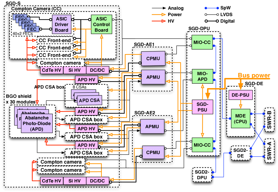
The front-end electronics of the Compton camera consists of four groups of 42 Front-End Cards (FECs) and an ASIC Driver Boards (ADBs), and an ASIC Control Board (ACB). Two FECs are connected back to back at the corner of each Si and CdTe trays, and are read out in daisy chain. FECs for the CdTe modules on the side have six ASICs that are daisy-chained on each board. Forty FECs from the Si/CdTe trays and two FECs from the CdTe modules on the side are connected to an ADB, which is located on the side of the Compton camera. Eight FECs (eight ASICs) are daisy-chained for Si/CdTe trays, resulting in 7 groups of ASICs for each side, 5 for Si/CdTe trays (8 ASICs each) and 2 for side-CdTe (6 ASICs each). Only digital communication is required between ADBs and FECs and all digital signals are differential to minimize the EMI (electro magnetic interference). Digital signals that are not used frequently are single ended between the ADB and the ACB due to constraints on the cable pin count. The ADB detects excess current of each ASIC group in order to protect ASICs from latch-ups due to highly ironizing radiation or other origins. We can recover ASICs from latch-ups by cycling the power supply.
ASICs are controlled by an FPGA on the ACB (one board per Compton camera). Functions of the ACB include: loading ASIC registers, sending a trigger to MIO and hold signals to ASICs with proper delays upon reception of triggers from ASICs, controlling analog-to-digital conversion on ASICs and data transfer from ASICs, halting data acquisition process if MIO cancels the trigger, formatting data from ASICs and send it to MIO, counting triggers and monitoring dead time.
CPMU functions include control of power switches and power supply voltages, monitor of power supply voltages and temperature. Remote HV (high voltage) bias power supplies are controlled via slow serial data link. We plan to ramp up and down bias power supply for the safety of the front-end electronics in the normal power up and down procedure. However, appropriate low pass filters should be placed between each sensor and the bias power supply so that any sudden change of the HV due to unforeseen reasons does not destroy front-end electronics connected to the sensors.
The APMU receives APD signals from APD CSAs and digitize them with flash ADCs. Digitized values are continuously monitored by an FPGA on the APMU. The FPGA differentiates the APD signal and issues a trigger when the differentiated signal is above a certain threshold. The time constant of the differentiation has to be optimized based on sampling frequency and the rising time of the CSA. Slightly more sophisticated algorithm is used to calculate more accurate pulse height information given the trigger timing of the Compton camera. Other APMU functions include HK such as control of power switches and power supply voltages, monitor of power supply voltages and temperature. Remote HV power supplies for APD are controlled via slow serial data link.
MIO functions include: recording event time tag, assemble veto information upon reception of trigger signals from Compton camera, sending trigger cancel within 10 s if necessary based on veto information, managing dead time, veto signals from APMU and ASIC registers which includes checking SEU bit from ASIC data, formatting data including sensor data, time tag, veto hit pattern, and send them to MIO, and controlling CPMU including reception of HK data from CPMU.
Communications between the Compton camera and MIO, and that between CPMU/APMU and MIO are handled via 3-line (CLK, DATA, STRB) serial protocol on LVDS physical layer. We have two additional real-time LVDS lines dedicated for trigger and trigger acknowledgement signals between CPMU and MIO. We also have dedicated LVDS lines to issue two types of veto signals between APMU and MIO.
5 Expected Scientific Performance
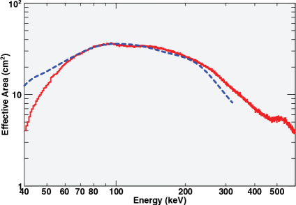
Effective area, non X-ray backgrounds, and sensitivities are evaluated by Geant4-based Monte Carlo simulations. The solid line in Figure 12 (a) shows the effective area as a function of the incident energy for the current SGD design. Maximum effective area of more than 30 cm2 is realized at around 80–100 keV, which corresponds to 15% reconstruction efficiency since the geometrical area of the SGD is 210 cm2. The effective area at low energies is suppressed due to the photo-absorption in Si while the loss at high energies is due to multiple-Compton events, which can be recovered by improved reconstruction algorithm. The dotted line in Figure 12 (a) shows the inverse of minimum detectable polarization (MDP) in arbitrary units assuming no background. The polarization sensitivity falls off slower at low energies and faster at high energies due to lower modulation factor resulting from more forward scattering at higher energies. This result indicates that SGD is sensitive to the polarization in the 50–200 keV energy band.
| (a) | (b) |
|---|---|
 |
 |
| (a) | (b) |
|---|---|
 |
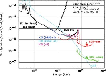 |
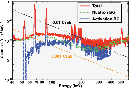
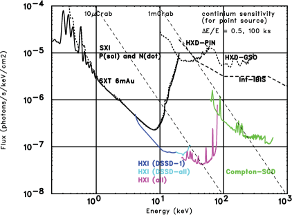
Main in-orbit background components of the SGD are expected to be activations induced during the SAA passages and elastic scatterings of albedo neutrons, at the expected orbit of ASTRO-H (altitude of 550 km with an inclination angle of 31∘). These background events can be heavily suppressed by a combination of multi-layer low-/high- sensor configuration, active shield, and the background rejection based on the Compton kinematics. The remaining background level is estimated to be much lower than any past instrument as shown in Figure 12 (b). The neutron background (green dotted curve) is estimated by the simulation assuming the neutron spectrum described in Ref. 16. The flux of the neutron background is scaled by a factor of two based on the background studies of the Suzaku hard X-ray detector [17]. The spectrum of the activation background (blue dashed curve) is estimated from experimental results on the radioactivities induced by mono-energetic protons [18]. The flux is scaled by a rejection factor expected from constraints by the Compton kinematics. The signal fluxes corresponding to 1/100 and 1/1000 of the Crab brightness are overlaid in black and orange dotted straight lines, respectively. This clearly illustrates that the expected background in SGD varies from 1/1000 to 1/100 of the Crab brightness in the 50–400 keV band. Fig. 13 shows 3 sensitivity for three instruments in the ASTRO-H mission, the SXI, HXI and SGD, for continuum emission from (a) point sources and (b) extended sources () with an observation time of 100 ks and comparison with other instruments. (Sensitivity depends on the bandwidth of each point and observation time, and can be lower than the background level with sufficient statistics.) SGD represents great improvement in the soft gamma-ray band compared with the currently operating INTEGRAL[19] or Suzaku HXD, and extends the bandpass to well above the cutoff of hard X-ray telescopes, which in turn allows us to study the high energy end of the particle spectrum. Combined with the SXI and the HXI on board the ASTRO-H, SGD realizes unprecedented level of sensitivities from soft X-ray to soft gamma-ray band.
| (a) | (b) |
|---|---|
 |
 |
| (a) | (b) |
|---|---|
 |
 |
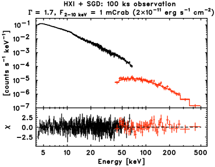
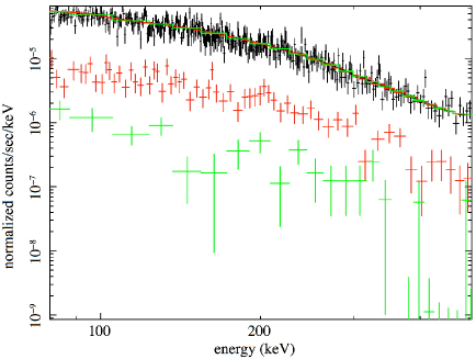
A simulation results shown in Figure 14 (a) demonstrate that spectral index can be measured within 10% error for a 100 ks observation of a source with 1/1000 of the Crab brightness in 2–10 keV and power law index of 1.7 using the current SGD design parameters. Another type of SGD target is supernova remnants where we can study nature of particle accelerations. Cas A is one of the most promising SNR for the SGD since sizable non-thermal bremsstrahlung emission is expected in the SGD band. Figure 14 (b) shows simulation results for observation of non-thermal bremsstrahlung from a supernova remnant, Cas A, which confirms that SGD can determine the magnetic field of Cas A with a 100 ks observation. This measurement will have significant implications on modeling of multi-wavelength observations since a model with leptonic origin predicts mG while a hadronic model prefers mG.
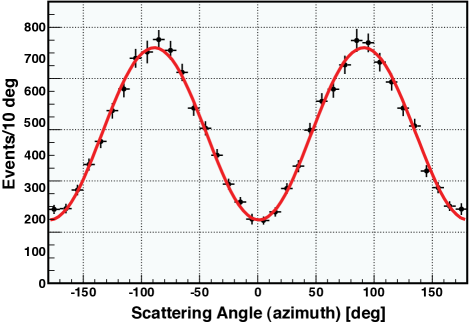
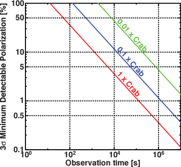
The polarization signature of incident gamma-ray is detected by the modulation of the azimuth angle distribution of Compton scattering in SGD as shown in Figure 15 (a) for a 100%-polarized source. A fit to yields %, where is the modulation factor which is proportional to the polarization degree and is the angle of the polarization vector. Using the modulation factor obtained here and the background level described above, we can calculate the MDP (minimum detectable polarization) analytically assuming no systematic effect from uneven backgrounds and uncertainties of the detector response. Figure 15 (b) shows the MDP as a function of the observation time for sources with 1, 1/10 and 1/100 of the Crab brightness, which can be parametrized as , and , respectively, where is the observation time in seconds. We can conclude that SGD can detect polarization from sources down to a few of the the Crab brightness with a polarization degree of several % in a few ks of observation time.
6 Summary
The Soft Gamma-ray Detector (SGD) onboard the next Japanese X-ray astronomy satellite ASTRO-H is designed to measure spectra of celestial sources with 1/1000 of Crab brightness in the 40–600 keV energy band, which is the highest end of the ASTRO-H energy coverage. The sensitivity of the SGD presents more than an order of magnitude improvement in the soft gamma-ray band as compared with the currently operating INTEGRAL or Suzaku HXD instruments. Combined with the soft and hard X-ray imagers (SXI and HXI) on board of ASTRO-H, the SGD realizes unprecedented level of sensitivities from soft X-ray to soft gamma-ray band. A key to achieve such sensitivity is a low background realized by a combination of the Compton camera surrounded by the BGO active shield where the incoming photon angle constrained by Compton kinematics is required to be consistent with the narrow field view of the active shield and passive collimator. The SGD is also capable of measuring polarization of celestial sources brighter than a few of the Crab Nebula, polarized above the 10%. This capability is expected to yield polarization measurements in several celestial objects, providing new insights into properties of soft gamma-ray emission processes.
The combination of low- (Si) and high- (CdTe) sensors allows us to employ appropriate sensor materials to lower the energy threshold, to minimize Doppler broadening while maximizing absorption efficiencies of the scattered photons. The low-/high- arrangement also suppresses contributions from neutron and activation backgrounds.
The SGD successfully completed preliminary design review in May 2010 and is currently in the detailed design phase. The ASTRO-H is expected to be launched in early 2014.
References
- [1] Takahashi, T. et al., “The NeXT X-ray mission, new exploration X-ray telescope,” in [UV to Gamma-Ray Space Telescope Systems ], SPIE 7011, 14T (2008).
- [2] Takahashi, T., Mitsuda, K., Kelley, R. L., et al., “The ASTRO-H mission,” in [Space Telescopes and Instrumentation 2010: Ultraviolet to Gamma Ray ], SPIE 7732 (2010).
- [3] Takahashi, T., Kamae, T., and Makishima, K., “Future hard X-ray and gamma-ray observations,” in [New Century X-ray Astronomy, ASP (Astronomical Society of the Pacific Conference Series) ], 251, 210–213 (2002).
- [4] Takahashi, T., Nakazawa, K., Kamae, T., Tajima, H., Fukazawa, Y., Nomachi, M., and Kokubun, M., “High resolution CdTe detectors for the next generation multi-Compton gamma-ray telescope,” in [X-ray and Gamma-ray Telescopes and Instruments for Astronomy, SPIE ], Truemper, J. E. and Tananbaum, H. D., eds., 4851, 1228–1235 (2002).
- [5] Takahashi, T., Makishima, K., Fukazawa, F., Kokubun, M., Nakazawa, K., Nomachi, M., Tajima, H., Tashiro, M., and Terada, Y., “Hard X-ray and Gamma-ray detectors for the NeXT mission,” New Astro. Rev. 48, 309–313 (2004).
- [6] Takahashi, T., Awaki, A., Dotani, T., Fukazawa, Y., Hayashida, K., Kamae, T., Kataoka, J., Kawai, N., et al., “Wide-band X-ray imager (WXI) and soft gamma-ray detector (SGD) for the NeXT mission,” in [UV and Gamma-Ray Space Telescope Systems ], SPIE 5488, 549–560 (2004).
- [7] Kokubun, M. et al., “Hard X-ray imager HXI for the NeXT mission,” in [UV to Gamma-Ray Space Telescope Systems ], SPIE 7011, 21K (2008).
- [8] Tajima, H., Kamae, T., Madejski, G., Mitani, T., Nakazawa, K., Tanaka, T., Takahashi, T., Watanabe, S., et al., “Design and performance of the Soft Gamma-ray Detector for the NeXT mission,” IEEE Trans. Nucl. Sci. 53, 2749–2757 (2005).
- [9] Takahashi, T. and Watanabe, S., “Recent progress in CdTe and CdZnTe detectors,” IEEE Trans. Nucl. Sci. 48, 950–959 (2001).
- [10] Watanabe, S., Tanaka, T., Nakazawa, K., Mitani, T., Oonuki, K., Takahashi, T., Takashima, T., Tajima, H., Fukazawa, Y., Nomachi, M., Kubo, S., Onishi, M., and Kuroda, Y., “A Si/CdTe semiconductor Compton camera,” IEEE Trans. Nucl. Sci. 52, 2045–2051 (2005).
- [11] Watanabe, S., Ishikawa, S., Aono, H., Takeda, S., Odaka, H., Kokubun, M., Takahashi, T., Nakazawa, K., Tajima, H., Onishi, M., and Kuroda, Y., “High energy resolution hard X-ray and gamma-ray imagers using CdTe diode devices,” IEEE Trans. Nucl. Sci. 56, 777–782 (2009).
- [12] Takeda, S., Aono, H., Okuyama, S., n. Ishikawa, S., Odaka, H., Watanabe, S., Kokubun, M., Takahashi, T., Nakazawa, K., Tajima, H., and Kawachi, N., “Experimental results of the gamma-ray imaging capability with a Si/CdTe semiconductor Compton camera,” IEEE Trans. Nucl. Sci. 56, 783–790 (2009).
- [13] Kamae, T., Ezawa, H., Fukazawa, Y., M, H., Idesawa, E., Iyomoto, N., et al., “Astro-E hard X-ray detector,” Proc. SPIE 2806, 314 (1996).
- [14] Toker, O., Masciocchi, S., Nygård, E., Rudge, A., and Weilhammer, P., “VIKING, a CMOS low noise monolithic 128 channel frontend for Si-strip detector readout,” Nucl. Instrum. Methods A 340, 572–579 (1994).
- [15] Tajima, H., Nakamoto, T., Tanaka, T., Uno, S., Mitani, T., do Couto e Silva, E., et al., “Performance of a low noise front-end ASIC for Si/CdTe detectors in Compton gamma-ray telescope,” IEEE Trans. Nucl. Sci. 51, 842–847 (2004).
- [16] Armstrong, T. W. et al. J. Geophys. Res. 78, 2715 (1973).
- [17] Fukazawa, Y. et al., “Modeling and reproducibility of Suzaku HXD PIN/GSO background,” Pub. of Astro. Soc. of Japan 61, S17 (2009).
- [18] Murakami, M., Kobayashi, Y., Kokubun, M., Takahashi, I., Okada, Y., Kawaharada, M., Nakazawa, K., Watanabe, S., Sato, G., Kouda, M., Mitani, T., Takahashi, T., Suzuki, M., Tashiro, M., Kawasoe, S., Nomachi, M., and Makishima, K., “Activation properties of schottky CdTe diodes irradiated by 150 MeV protons,” IEEE Trans. Nucl. Sci. 50, 1013–1019 (2003).
- [19] Winkler, C., Courvoisier, T. J.-L., Di Cocco, G., Gehrels, N., Giménez, A., Grebenev, S., Hermsen, W., Mas-Hesse, J. M., Lebrun, F., Lund, N., Palumbo, G. G. C., Paul, J., Roques, J.-P., Schnopper, H., Schönfelder, V., Sunyaev, R., Teegarden, B., Ubertini, P., Vedrenne, G., , and Dean, A. J., “The INTEGRAL mission,” Astronomy and Astrophysics 411, L1–L6 (2003).