Stacking and band structure of van der Waals bonded graphane multilayers
Abstract
We use density functional theory and the van der Waals density functional (vdW-DF) method to determine the binding separation in bilayer and bulk graphane and study the changes in electronic band structure that arise with the multilayer formation. The calculated binding separation (distance between center-of-mass planes) and binding energy are Å ( Å) and meV/cell ( meV/cell) in the bilayer (bulk), depending on the choice of vdW-DF version. We obtain the corresponding band diagrams using calculations in the ordinary generalized gradient approximation for the geometries specified by our vdW-DF results, so probing the indirect effect of vdW forces on electron behavior. We find significant band-gap modifications by up to -1.2 eV (+4.0 eV) in various regions of the Brillouin zone, produced by the bilayer (bulk) formation.
pacs:
81.05.Uw,73.22.Pr,71.15.Mb,I Introduction
Selective modification of band gaps (band-gap engineering) by atomic-scale design of materials is a powerful concept in electronic and photonic development.BGE Band gaps can be altered by, for example, introducing dopants, defects or by exploiting finite size effects.defects ; finiteSize The physical origin of band-gap variations is a modification in the charge distribution in concert with wavefunction hybridization and modification.
Dispersive or van der Waals (vdW) interactionsvdWDFreview also alter the distribution of electronic charges and hence the electron band-structure. A direct effect is evident, for example, by considering the formation of the double-dipole configurationThonhauser2007 which is the electrostatic signature and inherent nature of a pure vdW binding.vdWDFreview ; Thonhauser2007 In addition, there are also indirect, geometry-induced effects of vdW binding on electron behavior. These indirect effects arise when two material fragments come close to one another, thereby changing the local electron environments as compared to isolated fragments. For example, vdW-binding can cause smaller amounts of net charge transfer within individual vdW-bonded fragments.Londero2010 Also, wavefunction hybridization will certainly arise when material fragments approach one another, even if this hybridization does not significantly contribute to the binding itself (in purely dispersive interaction). Wavefunction hybridization and Pauli exclusion cause scattering of the surface-state electrons in physiosorption of acenes and quinones on Cu, even if there is no net charge transfer.sliding ; sliding2
The strength of vdW interactions in surface/adatom systems (including adclusters or complete overlayers) can be controlled by the precise choice of the surface materialJacobssenGrapheneOnMetals ; RohrerPhD ; RohrerGrapheneOnSiC and by the surface morphology (flat, stepped, pyramidal, etc.).KelkkanenBenxeneOnMetals It is therefore important to quantify the extent to which van der Waals (vdW) bonding can modify the electron dispersion, that is, the band structure. Such a study is now possible, since recent development of the vdW density functional (vdW-DF) method Thonhauser2007 ; vdWDF ; vdWDF2 ; C09 enables systematic (theoretical) explorations of bonding in sparse materials within density functional theory (DFT).vdWDFreview
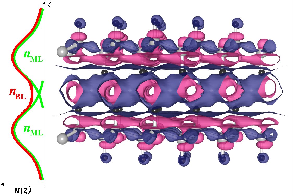 |
In this paper we investigate indirect, geometry-induced effects of vdW bonding on electronic structure. In particular we separately study the effects of (1) the enhanced charge density in regions where the tails of vdW-bonded material fragments overlap, see left panel of Fig. 1, (2) the hybridization of wave functions, and (3) the redistribution of charge density due to mechanisms that are not inherent to the vdW interaction (such as local displacements due to electrostatics and Pauli-repulsion), see right panel of Fig. 1.
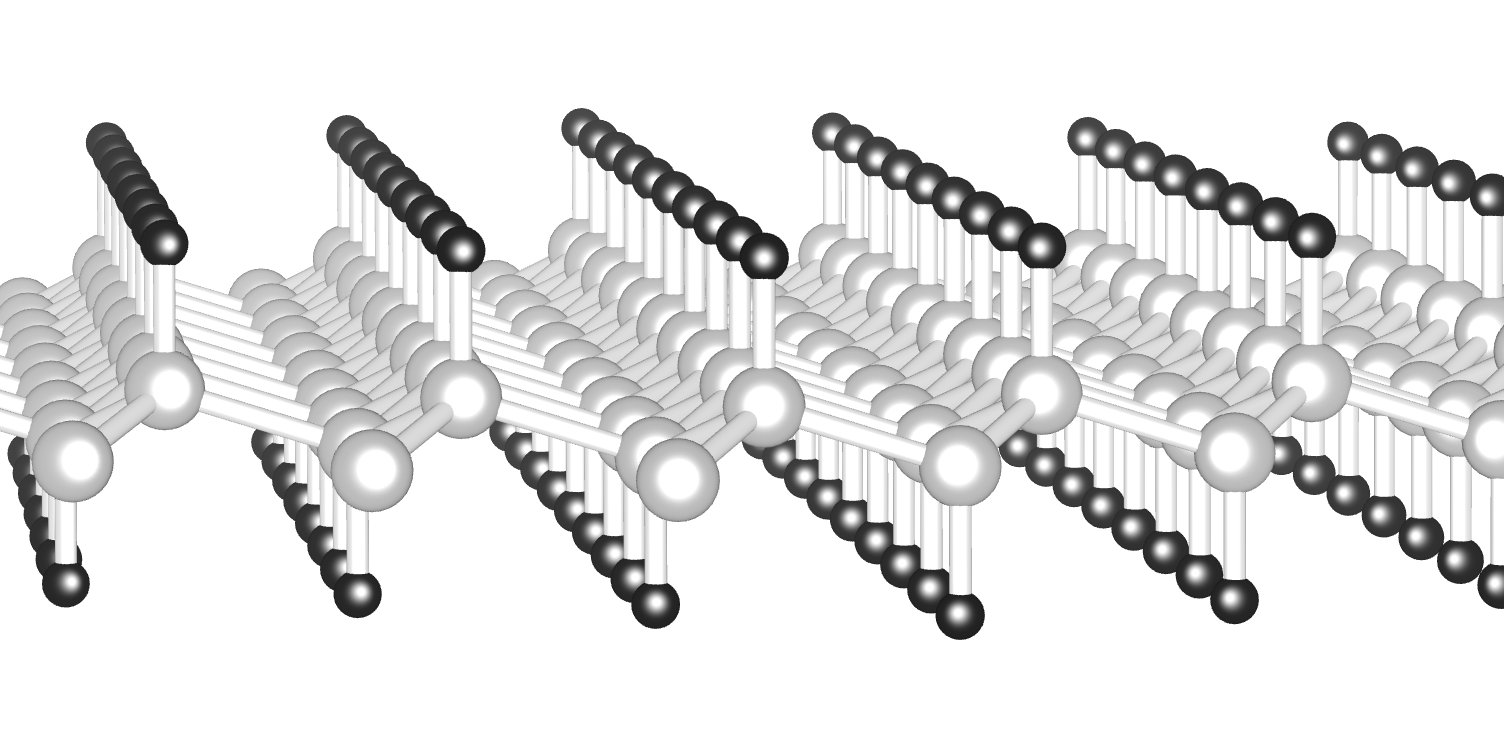
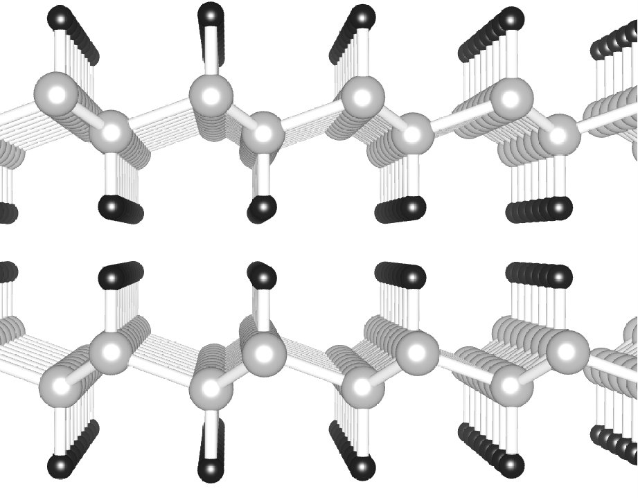
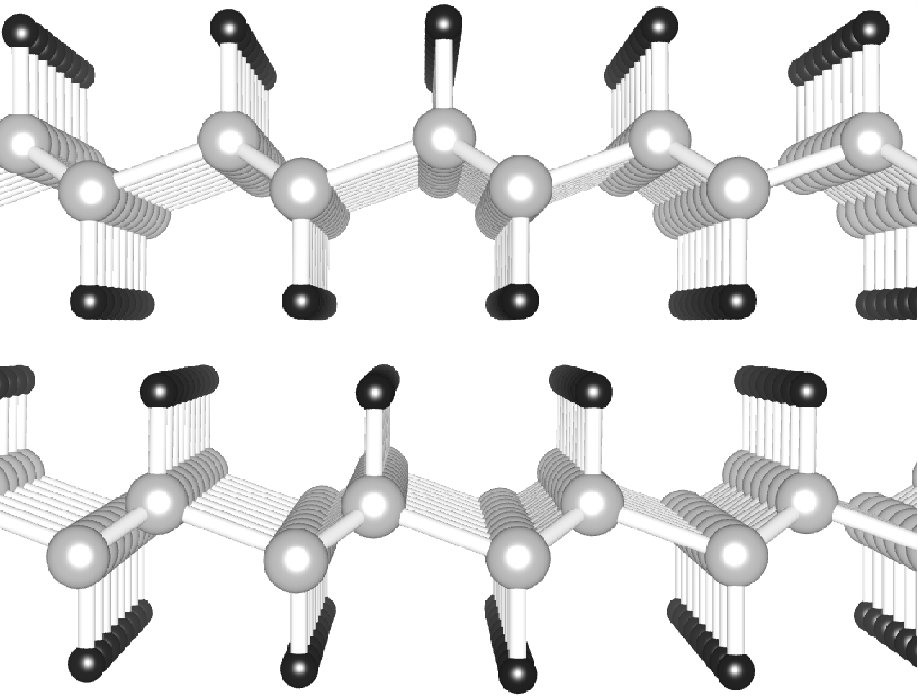
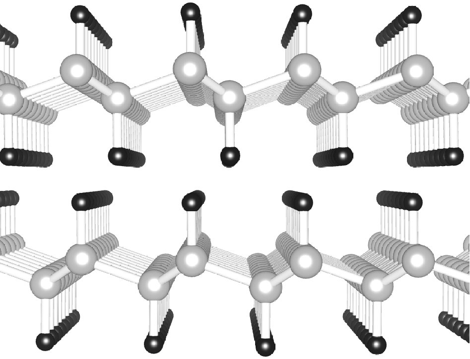
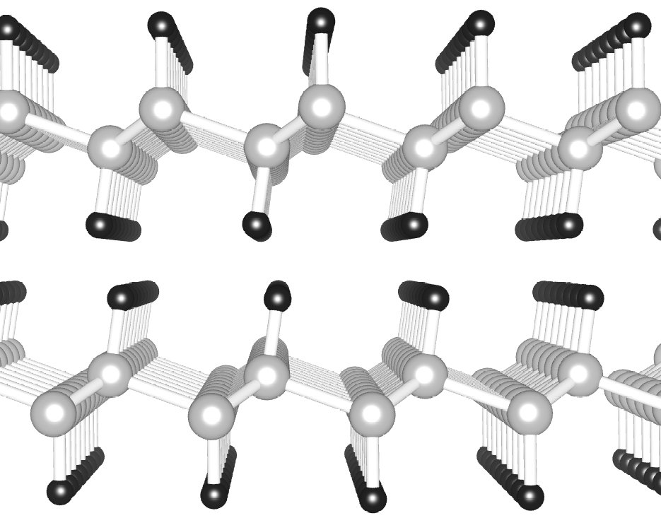
We focus on the band structure of layered systems of the macromolecule graphane,ref:Sofo_Graphane_2007 ; ref:Elias_Graphane_2009 a fully hydrogenated derivative of graphene.ref:Graphene The top panel of Fig. 2 shows the atomic structure of (the stable chair conformation of) monolayer (ML) graphane, consisting of a (slightly buckled) graphene backbone with H atoms attached in alternating fashion above and below the carbon plane. Bilayer graphane with possible high-symmetry structure shown in the bottom panels of Fig. 2 present a possible new system.BLGraphane1 ; BLGraphane2 In addition, we also include a study of a possible bulk-graphane crystal.
Graphane adds to the wealth of carbon-based materials that are considered as promising materials for near-future nanoelectronic devices.ref:Devices1 ; ref:Devices2 Pure graphene has a zero band gap and extraordinary conduction properties. Electronic devices, however, also require semiconducting and insulating materials. Such materials can be obtained from pure graphene as derivatives either in the form of graphene nanoribbonsGNRExp ; GNRModel or by chemical modification through adsorbates.ChemicalModification ; BGE_Eriksson Monolayer graphane belongs to the last-mentioned group of derivatives. DFT calculations predict a large band-gap semiconductor nature;ref:Sofo_Graphane_2007 the more advanced GW methodGW predicts an insulating nature.ErikssonGW Graphane has been proposed theoretically to serve as a natural host for graphene quantum dotsGraphaneQdots or graphene nanoribbons for nanoroads.GraphaneGrapheneJunc Furthermore, doped graphane has been recently predicted to be a high- superconductor.hTc-SC_graphane Such potential application of the graphane structure makes it interesting to explore possibilities to (locally) modify the the electronic behavior either by selective hydrogen removalErikssonGW ; GraphaneQdots ; GraphaneGrapheneJunc or by geometry-induced band-structure modifications.
II High-symmetry graphane bilayers
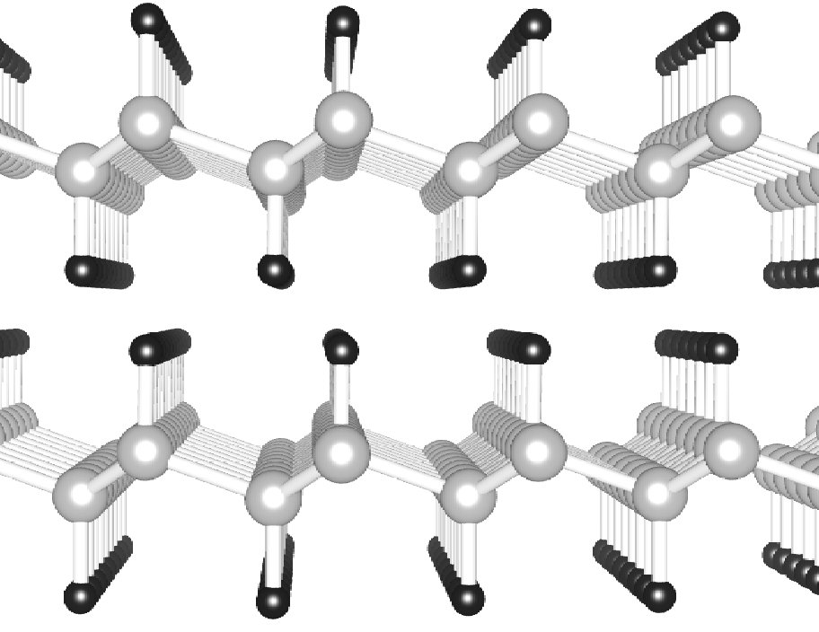
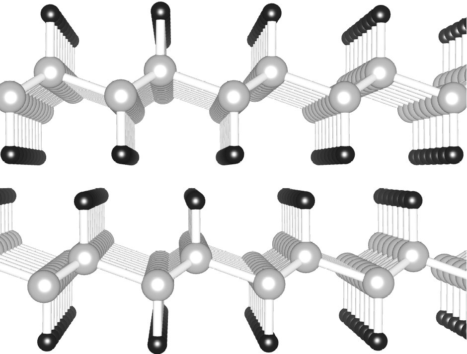
The set of lower panels in Fig. 2 shows all six high-symmetry arrangements of bilayer (BL) graphane. These can be grouped into two different types. In -type BL, the graphane sheets are interlocked with each other. In -type BL, the H atoms from different graphane sheets (located between the sheets) sit on top of each other. We calculate and compare all of these configurations that make up the - and -type sets of stacking configurations.
The set of different (high-symmetry) arrangements for the BL systems are found as follows. We label the sheets according to the location of vacancy in the C backbone in the unit cell (, , or sites). In addition, the distortion of the C backbone along the -direction ( or ) of the first occupied C site (counted along the main diagonal starting from the vacancy stacking) is indicated as a subscript label. In all BL, the first layer can be arbitrarily chosen to be an layer. The second layer is placed on top of the first one of the following actions: (i) copying the bottom layer and moving it along the -direction (); (ii) flipping the bottom layer and moving it along the -direction (); (iii) as in (i) and additionally moving it along the long diagonal of the 2D graphane lattice by one third (); (iv) as (ii) and additionally moving it along the long diagonal of the 2D graphane lattice by one third (); (v) as in (i) and additionally moving it along the long diagonal of the 2D graphane lattice by two thirds (); (vi) as in (ii) and additionally moving it along the long diagonal of the 2D graphane lattice by two thirds ().
| -type bilayers | -type bilayers | |
 |
 |
 |
 |
 |
 |
III Computational Method
III.1 vdW binding
We map out the energy variation of bilayer (bulk) graphane as a function of the separation between two graphane sheets (the -parameter of the bulk unit cell) using (non-selfconsistent) vdW-DF calculations. For BL, we employ supercells with our optimized 11 graphane in-plane lattice parameters [, with ] and a height of 30 Å. For the bulk, we optimize the -parameter of the periodic unit cell [] starting from the optimal value of the BL separation.
Our calculations combine selfconsistent DFT calculations in the generalized gradient approximation (GGA) with three (non-selfconsistent) versions of the vdW-DF method. The GGA calculations are performed with the planewave pseudopentialPseudopotentials code Dacapo,Dacapo using PBEPBE for exchange and correlation. We use a planewave cutoff of eV and a 441 (442) k-point samplingKpointSampling . The three versions of the vdW-DF method that we use are (i) the nonlocal correlation functional of Dion et al.vdWDF in conjunction with revPBErevPBE for exchange (vdW-DF1), (ii) the same correlation functional but with the exchange part of the C09 functionalC09 (vdW-DF1-C09), and (iii) the most recent version of the vdW-DF method, Ref. vdWDF2, (vdW-DF2). The latter version uses the refitted form of the PW86 functional (rPW86)PW86refitted for exchange. We obtain total energies as
| (1) |
Here, is the energy obtained from one of the non-local functionals of Refs. vdWDF, and vdWDF2, , and is given by
| (2) |
where is the VWN-LDAVWN correlation energy and the subscript ’v’ denotes the version of the exchange functional (revPBE, C09, or rPW86). We define the layer binding energy as
| (3) |
Here, is the distance between the center-of-mass planes in each graphane sheet of the monolayer.
Our numerical evaluation of Eq. (3) proceeds in the same way as described in Refs. sliding, and Method1, ; Method2, ; Method3, ; Method4, . In particular, because of a small but nonnegligible sensitivity of the nonlocal correlation on the exact positioning of atoms with respect to the density grid, we avoid a direct comparsion of for BL configurations with different ML separations. Instead we evaluate the layer-binding energy by comparing changes in the nonlocal correlation arising between the actual configuration and a reference that keeps the same alignment of atoms and grid points. Specifically, for all configurations we evaluate the change in nonlocal correlation as . Here is the nonlocal correlation energy of the full BL configuration (with one ML in P and one in Q) and () is the nonlocal energy of the configuration where one ML has been removed from Q (P) while the other is kept at precisely the same location P (Q) as in the BL configuration. Further details on our approach to increase the accuracy of vdW-DF are provided in Refs. sliding, and Method1, .
 |
 |
III.2 Band structure
We determine band structures with pure GGA calculations for various k points. We fix the BL separation (bulk -parameter) to the value calculated with vdW-DF, so probing indirect effects of vdW binding on electron behavior. The (selfconsistent GGA) input density for these (non-selfconsistent GGA) band-structure calculations is obtained using a planewave cutoff of 500 eV and a 20201 (20205) k-point samplingKpointSampling for the bilayer (bulk).
For the bilayer, the Brillouin zone (BZ) is two-dimensional and relevant k points are , and .BZpoints All special points are given in units of the reciprocal lattice vectors. We calculate the band variations along the paths , , and .
For the bulk, the BZ is three-dimensional. Therefore non-zero values of are important and we also calculate the band variations along , , and . Here, the special points are , , and .BZpoints
| bilayer graphane | |||
|---|---|---|---|
| vdW-DF1 | vdW-DF2 | vdW-DF1-C09 | |
| [Å] | 5.0 | 4.75 | 4.5 |
| [meV/cell] | 78 | 77 | 101 |
| at [eV] | 3.46 (-0.08) | 3.53 (-0.01) | 3.61 (+0.07) |
| at K [eV] | 11.86 (-0.30) | 11.75 (-0.41) | 11.61 (-0.55) |
| at M [eV] | 10.40 (-0.46) | 10.31 (-0.55) | 10.24 (-0.62) |
| bulk graphane | |||
| vdW-DF1 | vdW-DF2 | vdW-DF1-C09 | |
| [Å] | 4.8 | 4.7 | 4.5 |
| [meV/cell] | 93 | 94 | 127 |
| at [eV] | 7.23 (+3.69) | 7.50 (+3.96) | 8.01 (+4.47) |
| at K [eV] | 12.77 (+0.61) | 12.83 (+0.67) | 12.66 (+0.50) |
| at M [eV] | 10.00 (-0.86) | 9.95 (-0.91) | 9.85 (-1.01) |
| at A [eV] | 3.52 (-0.02) | 3.62 (+0.08) | 3.88 (+0.34) |
| at H [eV] | 11.63 (-0.53) | 11.58 (-0.58) | 11.48 (-0.68) |
| at L [eV] | 11.27 (+0.41) | 11.27 (+0.41) | 11.28 (+0.42) |
 |
IV Results: Predicted properties of bilayer and bulk graphane
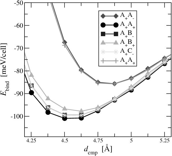
Figure 3 shows the calculated variations in layer-binding energies as functions of the separation between the center-of-mass planes (’cmp’) of the two graphane monolayers (ML) in a bilayer (BL). The top panel compares the energy variations for the configurations with different stackings using vdW-DF1-C09. The energy variations split according to the grouping into - and -type configurations. The -type configurations have a smaller binding separation and a higher binding energy; the stacking shows the strongest bonding.PES
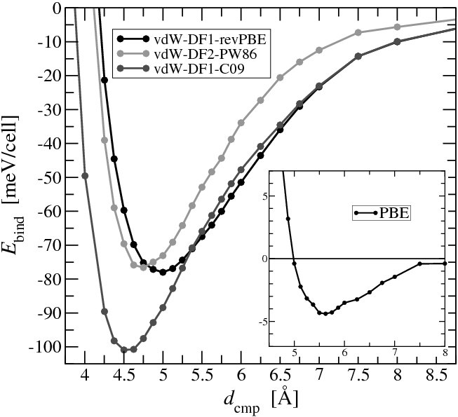
The bottom panel compares the energy variations of the BL for vdW-DF1, vdW-DF1-C09, and vdW-DF2. Qualitatively, all functionals yield the same energy variations. The insert shows the energy variation for the configuration obtained from pure PBE calculations and illustrates that no meaningful binding is predicted without an account of vdW forces.
Table 1 lists and compares numerical results for the calculated binding separations and layer-binding energies for the BL. The binding separations and energies range from 4.5 Å to 5.0 Å and 75 meV/cell to and 102 meV/cell, depending on the version of vdW-DF.LDAcomment The binding energy is comparable to that in a graphene BLref:GraphitevdW (94 meV using vdW-DF1).
Table 1 also lists the calculated lattice constant and the corresponding layer-binding energies for a fictitious bulk crystal of graphane. It is possible that such a 3D graphane system might eventually be synthesized. We here present predictions of the expected structure, using our analysis of stacking in the BL as starting point. In particular we focus on stacking and find that the lattice constant essentially coincides with in the bilayer. The binding energy is slightly increased in the bulk and varies between 93 eV and 127 meV. These numbers also compare to the binding in graphiteref:GraphitevdW (100 eV using vdW-DF1).
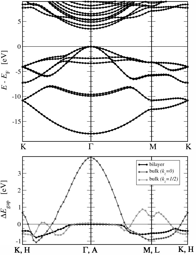
The top panel of Fig. 4 presents the overall PBE band-diagram for the stacked graphane BL at the binding separation predicted by vdW-DF2. Corresponding band diagrams at vdW-DF1 or vdW-DF1-CO binding separations are qualitatively similar. Apart from the fact that each band occurs as a pair of bands, the band structure also agrees qualitatively with that of the ML (see, for example, Ref. ref:Sofo_Graphane_2007, ).
The bottom panel of Fig. 4 summarizes some differences between the BL (bulk) and the ML, documenting the changes occurring in the -dependent band gap with the BL (bulk) formation. We plot the differences along , , and . In addition, for the bulk, we also plot . Here, is along , , and in the bulk; is the corresponding k point along , , and in the ML (and therefore , , while and ). A summary of the numerical values of band gaps at the special points (calculated with various choices of vdW-DF and corresponding BL binding separations or bulk lattice constants ) and their deviations from the corresponding values in the ML is given in Table 1.
We find large modifications of the band structure, indirectly induced by the vdW interactions and summarized by the -dependent band-gap differences. In the BL, the direct band gap can deviate by up to eV (between K and ) with respect to the ML gap (see bottom panel of Fig. 4). In the bulk, deviations can be as large eV ( eV) in some regions of the Brillouin zone (BZ) near the H point ( point).
V Discussions: Bilayer graphane
Focusing on the direct band gap in BL graphane, we find modifications that are strongly -dependent. At the K and M points (and in other regions), the modifications are significant. At the point, where the gap is smallest in the ML (and in the BL), no modifications occur, rendering the BL system electronically similar to the ML system. Nevertheless, qualitative understanding of the origin of the different modifications in the various regions is important to gain further insight into the relevance of vdW interactions for materials band-structure.
In the following, we explore the band-gap modifications upon formation of graphane BLs in more detail. We focus on the indirect, geometry-induced effects of vdW binding outlined in Fig. 1: the effect of a modified electronic environment in the region between the MLs that form the BL arising from a superposition of two ML electron densities (see left panel); the effect of self-consistent charge rearrangements (on the GGA level) of this superpositioned density (see right panel); the effect of potential hybridization of wave functions (WFs) (not shown in the figure).
Our analysis suggests that the band-gap modifications should be interpreted as a concerted interplay between WF hybridization and electrostatic interaction between the hybridized WFs with the modified environment. The relevant WFs are unoccupied conduction-band (CB) WFs. Self-consistent (SC) charge rearrangements (with respect to the superposition of ML densities) do not play a significant role.
V.1 Band-origin of gap reduction
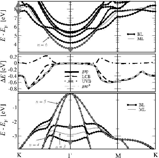
In the mid-panel of Fig. 5, we show that the main contribution to the observed band-gap variation comes from the lower conduction-band (LCB). We plot the variations of the upper valence-band (UVB) energies (dashed-dotted curve) and of the LCB energies (dashed curve),
| (4) |
Here is the energy of the highest (occupied) valence band (XXX = UVB) or the energy of the lowest (unoccupied) conduction band (XXX=LCB) at in the BL/ML and is the Fermi level in the BL/ML. (The Fermi level is here defined by the energy of the highest occupied state).
We find that is typically much larger than . The latter is essentially zero. In the UVB, nonzero contributions to the band-gap modifications are only found in small regions. As can be seen from the bottom panel of Fig. 5 where we contrast BL VBs with ML VBs, the topmost BL UVBs are non-degenerate there, indicating WF hybridization. Nevertheless, in regions where is large, only contributes. Thus, we assign the modifications of the band-gap variation in the BL primarily to the modifications in the LCB energy variation.
V.2 Self-consistent charge rearrangements
In the mid-panel of Fig. 5 we also contrast band-structure modifications obtained from the SC BL charge density with band-structure modifications obtained from the non-SC charge density, constructed as a superposition of ML densities. The solid black line (gap) corresponds to the SC case, the dashed light-gray line (gap∗) corresponds to the non-SC case. At the displayed resolution, the curves cannot be distinguished. We find that the differences between both band-gap variations are at the meV level. Thus, the charge rearrangementsChargeTransfer shown in the right panel of Fig. 1 do not appreciably contribute to the band-gap variation. In fact, this also applies for the overall band structure variation.
Further charge rearrangementsThonhauser2007 that are inherent to vdW forces (and require a SC vdW-DF calculations)Thonhauser2007 ; Soler ; GPAW are expected to be even smaller than those resulting at the the GGA level. The inherent rearrangements are not expected to be of importance for the band structure. This justifies our use of non-SC vdW-DF in this study of bilayer graphane.
V.3 Hybridization and concerted effects on kinetic and potential energy
In the remainder of this section we investigate the role of hybridization for the observed band-structure modifications. In the simplest picture of hybridization a bonding and antibonding hybrid WF can be formed when two degenerate atomic or layer WFs and approach each other,
| (5) |
If the actual BL WF equals or alternatively , its energy is shifted to lower energies. Similarily, if the actual BL WF equals or alternatively , its energy is shifted to lower energies. The energy shifts in such a simple picture of hybridization effects are due to a gain and a loss of kinetic energy.
This simple hydrogen-like picture of hybridization needs to be modified in the present case for two reasons. First, the unhybridized ML WFs are already complex objects possessing internal nodes. Second, the WFs live in a background effective potential . The hybrid WFs will then interact with this potential leading to further modifications of the actual bonding (B) and actual antibonding (A) WFs and . The actual hybrid WFs and will therefore no longer coincide with and , nor will their energy shift be only of kinetic nature.
We now move the discussion to a comparison of ML and BL graphane. For the ML, we denote the WFs by , where is the band index and k the wave vector. For the BL, is the bonding WF associated with two located on different sheets; is the antibonding WF.
These WFs (here collectively denoted by ) satisfy the Kohn-Sham equation
| (6) |
Here, is the effective potential (which, in general, is different for the ML and BL system), is the Fermi level (which may also be different in the ML or BL system) and the band energy of the WFs (also different in general). Accordingly, we can separate the kinetic- and potential-energy shifts of hybrid WFs as
| (7) | ||||
| (8) |
In the present analysis we focus on a quantitative evaluation of the per-orbital potential-energy shifts in Eq. (8) and on a qualitative account of the changes in the kinetic-energy term in Eq. (7). We replace the effective potential by the electrostatic potential (consisting of the Hartree potential and the atomic core potentials), neglecting effects from exchange and correlation, and give qualitative accounts of the changes in kinetic energies. A quantitative comparison of kinetic-energy shifts would be desirable but, since we are using pseudo-WFs, the evaluation of Eq. (7) is nontrivialPseudopotentials and beyond the present scope.
We obtain a qualitative analysis of the changes in kinetic energies by plotting the change of partial electron density associated with an (anti-) bonding BL WF
| (9) |
with respect to a sum of or difference between the corresponding ML WFs,
| (10) |
The differences
| (11) |
measure the extent to which the BL WFs experience a reduction or enhancement of kinetic energy with respect to a simple hybridization, Eq. (5).
| k | n | ||||
|---|---|---|---|---|---|
| in eV | |||||
| 2 (VB) | -0.17 | 0.14 | 0.20 | -0.34 | |
| 3 (VB) | -0.48 | 0.51 | 0.43 | -1.04 | |
| K | 6 (CB) | -0.37 | 0.31 | 0.37 | -0.51 |
| 6 (CB) | 0.00 | — | -1.07 | — | |
V.4 Hybridization in the valence band
Hybridization in the valence band is found, for example, around the point in the bands that correspond to band no 2 and 3 in the ML, see Figs. 4 and 5. We emphasize that the hybridization of the corresponding WFs is not a signature of binding. The energy splits are (essentially) symmetric and since both the bonding and the antibonding states are occupied, there is no (significant) net gain in total energy.
In Table 2, we list the total-energy shifts (obtained directly from our calculations) and the potential-energy contributions to these shifts for the corresponding WFs. Interestingly, we find that the electrostatic contributions to the energy shifts are positive for bonding BL WF whereas they are negative for the antibonding BL WF. The kinetic-energy gain (loss) must therefore be significantly larger than the loss (gain) in potential energy of the bonding (antibonding) BL WF to produce the ordering shown in the bottom panel of Fig. 5 (compare states identified by triangles at the point).
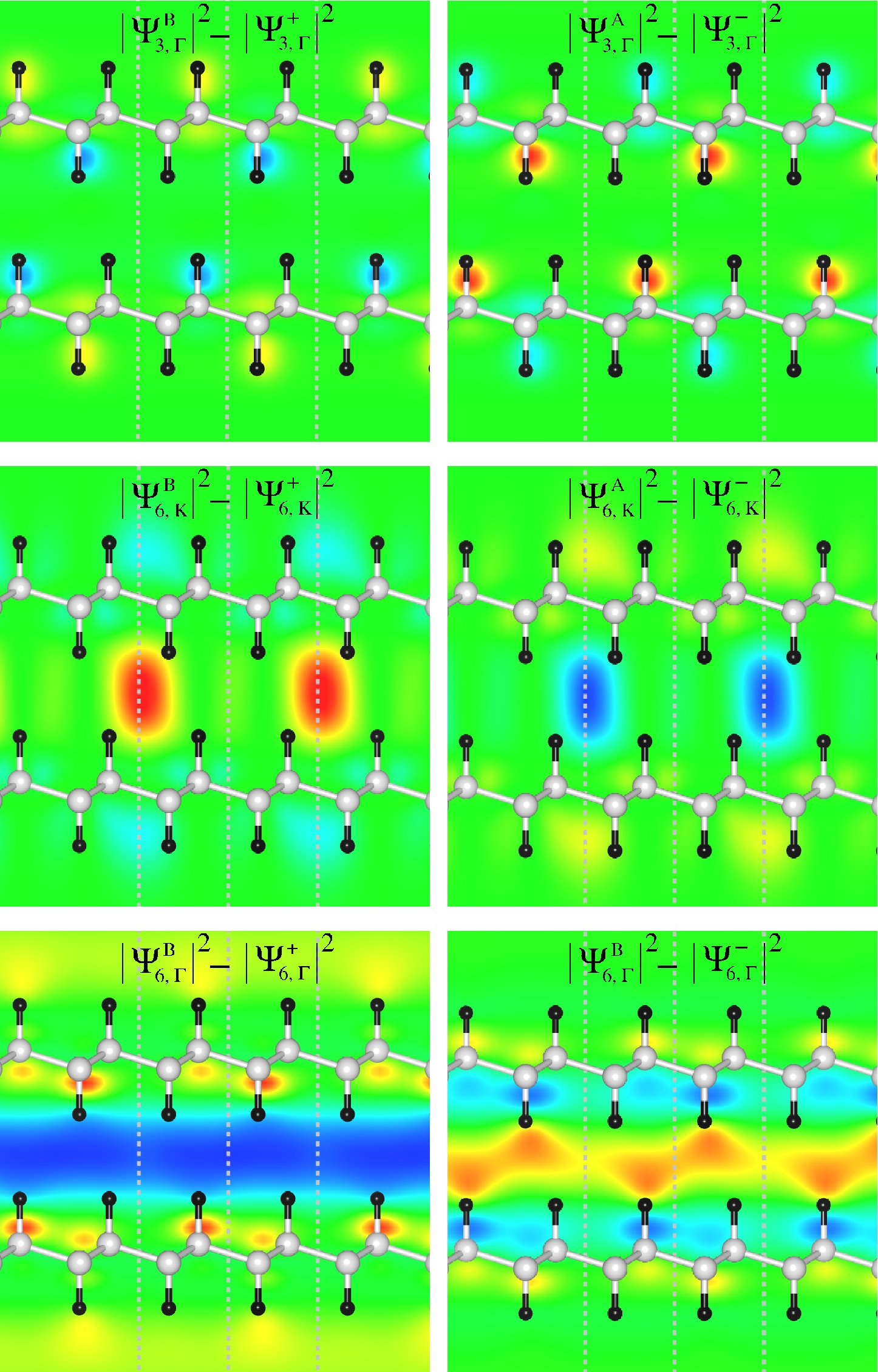 |
The top panels of Fig. 6 show sections (through the main diagonal of the unit cell) of the difference between the partial densities that correspond to the bonding and antibonding VB BL WFs at and the partial densities that correspond to the pure sum of (difference between) the corresponding ML WFs (with band index 3). The green color (indicating an absence of any decrease or enhancement relative to a simple hybridization) between the MLs in both panels shows that the BL WFs gains or looses kinetic energy. These kinetic-energy changes evidently more than make up the concerted changes in the potential-energy terms.
V.5 Conduction-band modifications
For the CB, we focus on the band-gap modifications and WFs at the points marked in the top panel of Fig. 5 (at K and ). At K, the total-energy splitting leads to the reduced band gap. As shown in Tab. 2, the potential-energy shift is positive for the bonding BL WF at K (marked with a downward triangle in Fig. 5) and negative for the antibonding BL WF (marked with an upward triangle). This observation is in line with those made at in the VB.
The mid-panels of Fig. 6 show the differences between partial density associated with the lowest bonding (next-lowest antibonding) CB BL WFs and the density associated with the pure sum of (difference between) the corresponding ML WFs at K. For the bonding BL WF, the partial density is increased between the two ML with respect to the pure sum of ML WFs. For the antibonding BL WF, the partial density is decreased with respect to the difference between the ML WFs. This indicates that the kinetic energy gain (loss) of the bonding (antibonding) BL WF is larger than within a simple hybridization picture where the hybrid WFs already possessing a kinetic energy gain (loss) with respect to an individual ML WF.
At , the contribution of the potential energy to the total shift of the lowest lying CB WF (marked with a square Fig. 5) is negative, see Table 2. In a simple hybridization picture one would expect a WF with a bonding nature and an additional decrease of kinetic energy. The vanishing shift in total energy, however, requires a kinetic-energy offset that compensates for the negative potential-energy shift. Specifically, one must therefore expect a more complicated hybridization of this BL WF.
The bottom panels of Fig. 6 show the difference between the partial density of the lowest CB BL WF and the pure sum of (left panel) and the pure difference between (right panel) the corresponding ML WFs at . The significantly negative value of the contours between the MLs in the left panel indicates that the BL WF at has a higher kinetic energy than the pure sum of ML WFs. Similarly, the kinetic energy is lower than in the difference between ML WFs, indicated by the positive value of the contours between the MLs in the right panel.
The contour plots show that the lowest CB BL WF at is not a simple hybridization of ML WFs. Also, we notice that the differences in the right panel are not as pronounced as the differences in the left panel. This suggests that the lowest CB BL WF at possesses rather an antibonding nature (although the lowest CB BL WF has a smaller kinetic energy than a simple antibonding hybridization). Such an antibonding nature is consistent with the vanishing total-energy shift and the negative potential-energy shift.
 |
VI Discussions: Bulk graphane
The most pronounced electronic difference between bulk graphane and ML or BL graphane is the fact that the A point takes over the role of the point, see Fig. 4. At A, the band gap is smallest in the bulk and the size of that gap coincides essentially with the size of the gap at in the ML or BL. Also, in the bulk, the deviations in the band-gap variations can be considerably larger than those in the BL, see bottom panel of Fig. 4. Here, we give a more detailed analysis of the overall band structure effects associated with graphane assembly into bulk.
In the the left panel of Fig. 7, we show the band diagram along , , and . Focusing on the CB, the bulk band structure is very different from that of the BL along the same path, see top panel of Fig. 4. In particular at the point, that gap is approximately twice as large as in the BL. Also, the band energy at K is considerably higher than in the BL. Only at M, we find similar band energies. Thus, the effect of vdW-bonding on local features of the band structure and related observable properties can be dramatic.
In the mid-panel of Fig. 7, we show show the band diagram along , , and . Again, the the bulk band structure is very different from that of the BL along the parallel path along , , and . The band energy at H is lower than at L, while it is the other way around at K and at M in the BL. Only around the point (corresponding to in the BL and ML cases) do the bulk and ML band diagram show similar features.
In the right panel of Fig. 7, we effectively combine the two diagrams from the left and mid-panel, calculating the band diagram for a would-be 2-layer unit cell at . The resulting band diagram shows the features of the BL band diagram and of the VB there is also a very good quantitative agreement. Therefore, the BL band-diagram can partly be understood as a zone-folded version of the bulk band-diagram.
VII Summary and Conclusion
This paper predicts and characterizes band-structure modifications produced indirectly as a geometry-induced effect of pure dispersive binding between two macromolecules in possible new material systems: bilayer and bulk graphane.BLGraphane1 ; BLGraphane2 Using non-selfconsistent vdW-DF calculations,vdWDFreview ; Thonhauser2007 ; vdWDF ; vdWDF2 ; C09 we determine the binding separation (-lattice parameter) and binding energies in vdW-bonded graphane bilayers (bulk). We use the calculated separations to obtain corresponding GGA-DFT band diagrams. Our results demonstrate that vdW interactions can significantly alter electron behavior, at least locally in the Brillouin zone. In graphane, the direct band gap is reduced (increased) by up to 1.2 eV (4 eV).
Our analysis shows that the origin of the band-gap modifications in this system is the concerted action of two geometry-induced effects. The first cause is the hybridization between unoccupied wave functions in the lowest conduction band. This effect generally leads to lower (higher) energy state for the bonding-type (antibonding-type) hybrid wave function, but not always, since the graphane wavefunctions can possess a more complex hybridization nature than what applies in the hydrogen-like case. The second cause is the modified electrostatic interaction between the hybrid wave functions and the electron density. This cause can either increase or decrease the energy gain (loss) in a bonding-type (antiboning-type) hybridization. Moreover, it may result into a modified hybrid wave-function where a pure bonding-type (antibonding-type) character is lost.
Our analysis also shows that selfconsistent charge rearrangements (on the GGA level) with respect to the ML density have no significant impact on the bandstructure. Additional charge rearrangements described by self-consistent vdW-DF calculationsThonhauser2007 are expected to be even smaller, justifying our use of non-selfconsistent vdW-DF.
The nature of conduction and optical absorption in BL graphane would be determined by the region around the point. There, the band structure of the bilayer essentially coincides with that of the monolayer. Therefore, we expect graphane multilayers to behave electronically similar to a graphane monolayer, at least for properties defined by a simple response. For bulk graphane, the behavior is more complicated. We emphasize that other vdW-bonded systems may exist where significant band-gap modifications arise at Brillouin-zone points having higher relevance for the electronic nature of the material.
Our results for BL graphane suggest that vdW forces can have non-negligible indirect effects on the overall band structure in layered or macromolecular materials. A similar effect can be found in V2O5,LonderoRohrer where traditional GGA severely overestimate the lattice constant and where vdW-DF provides a more accurate description.Londero2010 Furthermore, we notice that vdW binding of the intrinsic semimetal graphene to metalJacobssenGrapheneOnMetals or semiconductorRohrerPhD ; RohrerGrapheneOnSiC surfaces seems to generally lead to a shift of the Fermi level, rendering graphene a true metal. These observations together with the fact that the vdW binding strength in surface/adatom systems (and thus presumably the strength of the corresponding effect on the band structure) depends on the choice of the substrate materialJacobssenGrapheneOnMetals and on the substrate morphologyKelkkanenBenxeneOnMetals implies a possibility to exploit dispersive interactions also in band-gap engineering.
Finally, a comment on the accuracy of the predicted band-gap modifications is in order. GGA DFT typically severely underestimates the band gap in semiconductors or insulators. A possible remedy is the use of the GW method where the Kohn-Sham orbitals are used to construct the self-energy operator. The GW method also contains non-local correlations and therefore provides an alternative description of vdW interaction. GW calculations come at a considerably higher computational cost than that of vdW-DF, however. The procedure illustrated here, using vdW-DF calculations to determine binding morphologies followed by band-structure calculations might well also be adapted for GW, pursuing characterizations of band-structure effects in sparse matter.
Acknowledgment
We thank G. D. Mahan for encouragement and discussions. Support by the Swedish National Graduate School in Materials Science (NFSM), the Swedish Research Council (VR) and the Swedish National Infrastructure for Computing (SNIC) is gratefully acknowledged.
References
- (1) F. Capasso, Science 235, 172 (1987); F. Capasso, Thin Solid Films 216, 59 (1992).
- (2) V. H. Crespi, M. L. Cohen and A. Rubio, Phys. Rev. Lett. 79, 2093 (1997).
- (3) B. Xu and B. C. Pan, Phys. Rev. B 74, 245402 (2006).
- (4) D.C. Langreth, B.I. Lundqvist, S.D. Chakarova-Käck, V.R. Cooper, M. Dion, P. Hyldgaard, A. Kelkkanen, J. Kleis, Lingzhu Kong, Shen Li, P.G. Moses, E. Murray, A. Puzder, H. Rydberg, E. Schröder, and T. Thonhauser, J. Phys.: Condensed Matter 21, 084203 (2009).
- (5) T. Thonhauser, V. R. Cooper, S. Li, A. Puzder, P. Hyldgaard, and D. C. Langreth Phys. Rev. B 76, 125112 (2007).
- (6) E. Londero and E. Schröder, Phys. Rev. B 82, 054116 (2010).
- (7) K Berland, T.L. Einstein, and P. Hyldgaard Phys. Rev. B 80, 155431 (2009).
- (8) G. Pawin, K. L. Wong, K.-Y. Kwon, L. Bartels, Science 313, 961 (2006).
- (9) M. Vanin, J. J. Mortensen, A. K. Kelkkanen, J. M. Garcia-Lastra, K. S. Thygesen, and K. W. Jacobsen, Phys. Rev. B 81, 081408(R) (2010).
- (10) J. Rohrer, ”Formation stability and electronic structure of surfaces and int erfaces from first principles”, PhD Thesis, ISBN 978-91-7385-469-6, Chalmers University of Technology (2010).
- (11) J. Rohrer and P. Hyldgaard, unpublished.
- (12) A. Kelkkanen, B. I. Lundqvist and J. K. Norskov, accepted for publication in PRB.
- (13) M. Dion, H. Rydberg, E. Schröder, D. C. Langreth, and B. I. Lundqvist, Phys. Rev. Lett. 92, 246401 (2004).
- (14) K. Lee, É. D. Murray, L. Kong, B. I. Lundqvist, and D. C. Langreth, Phys. Rev. B 82, 081101(R) (2010).
- (15) V. R. Cooper, Phys. Rev. B 81, 161104(R) (2010).
- (16) J. O. Sofo, A. Chaudhari and G. D. Barber, Phys. Rev. B 75, 153401 (2007).
- (17) D. C. Elias, R. R. Nair, T. M. G. Mohiuddin, S. V. Morozov, P. Blake, M. P. Halsall, A. C. Ferrari, D. W. Boukhvalov, M. I. Katsnelson, A. K. Geim, and K. S. Novoselov, Science 323, 5914 (2009).
- (18) K. S. Novoselov, A. K. Geim, S. V. Morozov, D. Jiang, Y. Zhang, S. V. Dubonos, I. V. Grigorieva, and A. A. Firsov, Science 306, 666 (2004).
- (19) O. Leenaerts, B. Partoens, and F. M. Peeters, Phys. Rev. B 80, 245422 (2009).
- (20) V. I. Artyukhov and L. A. Chernozatonskii, J. Phys. Chem. A 114, 5389 (2010).
- (21) A. K. Geim and K. S. Novoselov, Nature Materials 6, 183 (2007).
- (22) A. K. Geim, Science 324, 1530 (2009).
- (23) G. Henkelman, A. Arnaldsson, and H. Jónsson, Comput. Mater. Sci. 36, 254 (2006)
- (24) K. Berland, Ø. Borck, and P. Hyldgaard, submitted to Comp. Phys. Comm., see also arXiv:1007.3305v1; Ø. Borck, unpublished.
- (25) M. Y. Han, B. Özyilmaz, Y. Zhang, and P. Kim, Phys. Rev. Lett. 98, 206805 (2007).
- (26) V. Barone, O. Hod, and G. E. Scuseria, Nano Lett. 6, 2748 (2006).
- (27) Schedin et al. Nat. Mater. 6, 652 (2007).
- (28) M. Klintenberg, S. Lebégue, M. I. Katsnelson, and O. Eriksson, Phys. Rev. B 81, 085433 (2010).
- (29) L. Hedin, Phys. Rev. 139, A796 (1965); F. Aryasetiawan and O. Gunnarsson, Rep. Prog. Phys. 61, 237 (1998).
- (30) S. Lebegue, M. Klintenberg, O. Eriksson, and M.I. Katsnelson, Phys. Rev. B 79 245117 (2009).
- (31) A. K. Singh, E. S. Penev and B. I. Yakobson, ACS Nano 4, 3510 (2010).
- (32) A. K. Singh and B. I. Yakobson, Nano Lett. 9, 1540 (2009).
- (33) G. Savini, A. C. Ferrari, and F. Giustino, Phys. Rev. Lett. 105, 037002 (2010).
- (34) D. Vanderbilt, Phys. Rev. B 41, 7892 (1990).
- (35) B. Hammer, O. H. Nielsen, J. J. Mortensen, L. Bengtsson, L.B. Hansen, A. C. E. Madsen, Y. Morikawa, T. Bligaard, A. Christensen, and J. Rossmeisl, available from https://wiki.fysik.dtu.dk/dacapo.
- (36) J. P. Perdew, K. Burke, and M. Ernzerhof, Phys. Rev. Lett. 77, 3865 (1996).
- (37) H. J. Monkhorst and J. D. Pack, Phys. Rev. B 13, 5188 (1976).
- (38) Y. Zhang and W. Yang, Phys. Rev. Lett. 80, 890 (1998).
- (39) E. D. Murray, K. Lee, and D. C. Langreth, J. Chem. Theory Comput. 5, 2754 (2009).
- (40) S.H. Vosko, L. Wilk, M. Nusair, Can. J. Phys. 58, 1200 (1980).
- (41) E. Ziambaras, J. Kleis, E. Schröder, and P. Hyldgaard, Phys. Rev. B 76, 155425 (2007).
- (42) S. D. Chakarova-Käck, E. Schröder, B. I. Lundqvist, and D. C. Langreth, Phys. Rev. Lett. 96, 146107 (2006).
- (43) K. Johnston, J. Kleis, B. I. Lundqvist, and R. M. Nieminen, Phys. Rev. B 77, 121404(R) (2008).
- (44) J. Kleis, E. Schröder, and P. Hyldgaard, Phys. Rev. B 77, 205422 (2008).
- (45) H. Ibach and H. Lüth, Solid-State Physics: An Introduction to Principles of Materials Science 3rd ed. (Springer-Verlag 2002).
- (46) We have also mapped out the vdW-DF potential energy landscape (PES) that arises when one of the graphane sheets is slightly displaced in various directions from this high-symmetry configuration. This stability test was performed for various layer separations around the binding separation predicted by vdW-DF2. On the PBE level, the displaced configurations essentially do not relax, reflecting the essentially flat PBE PES at these separations. However, adding the nonlocal vdW correction by evaluating Eq. (3), we find that the high-symmetry configuration possesses the lowest total energy of all considered systems.
- (47) We notice that full relaxation of the considered high-symmetry configurations using LDA also predicts the to be most favorable. Also, the predicted LDA binding separation of Å is in fair agreement with those predicted here by the various versions of vdW-DF (whereas the LDA-predicted layer-binding energy of meV/cell is considerably smaller). However, we stress that this correspondence with vdW-DF results coincidentally. LDA binding in systems which (like multilayer graphane) are bound by vdW forces has been assigned to unphysical long-range exchange interactions and LDA does not, by any means, contain vdW interactions, see J. Harris, Phys. Rev. B 31, 1770 (1985); E. D. Murray, K. Lee and D. C. Langreth, J. Chem. Theory Comput. 5, 2754 (2009) and references therein.
- (48) S. D. Chakarova-Käck, A. Vojvodic, J. Kleis, P. Hyldgaard, and E. Schröder, New J. Phys. 12 013017 (2010).
- (49) In the present case the charge rearrangements are not accompanied by any significant charge transfer. Our Bader analysis BaderAnalysis1 ; BaderAnalysis2 shows that the difference in charge before and after the charge rearrangement is e/atom. In cases where charge transfer takes place, see for example Ref. Londero2010, , such rearrangements may have more significance.
- (50) E. Londero and J. Rohrer, unpublished.
- (51) J. P. Perdew and W. Yue, Phys. Rev. B 33, 8800 (1986)
- (52) G. Román-Pérez and J. M. Soler, Phys. Rev. Lett. 103, 096102 (2009).
- (53) Selfconsistent vdW-DF is available in the opensource code GPAW,GPAWreview see https://wiki.fysik.dtu.dk/gpaw/index.html.
- (54) J. Enkovaara, C. Rostgaard, J. J. Mortensen et al. J. Phys.: Condens. Matter 22, 253202 (2010).