Single-charge escape processes through a hybrid turnstile in a dissipative environment
Abstract
We have investigated the static, charge-trapping properties of a hybrid superconductor—normal metal electron turnstile embedded into a high-ohmic environment. The device includes a local Cr resistor on one side of the turnstile, and a superconducting trapping island on the other side. The electron hold times, , in our two-junction circuit are comparable with those of typical multi-junction, , normal-metal single-electron tunneling devices. A semi-phenomenological model of the environmental activation of tunneling is applied for the analysis of the switching statistics. The experimental results are promising for electrical metrology.
1 Introduction
Currently, a growing interest is observed to the quantum sources of electrical current, based on a clocked transfer of the elementary charges. Developed for mesoscopic systems of small tunnel junctions, an orthodox theory of single-electron tunneling (SET) [1] has been used to describe the operation of the SET pumping devices (for a few examples, see Refs. [2, 3, 4]) in terms of cyclic sequences of the charge states with the charge values on the nodes being a multiple of the electron charge . The quantized current value is given by , where is the cycling frequency and is the number of electrons transferred in one cycle.
A more complete picture involves a broad scope of cotunneling leakage processes [5, 6] as well as the influence of the electromagnetic environment [7, 8] to explain the finite, often unexpectedly short decay times of the participating charge configurations, imposing a significant limitation onto the pumping accuracy. Accordingly, the rate of charge leakage across the whole device has been an important characteristic of any Coulomb blockade circuit (see, e.g., Refs. [3, 4, 9]). For example, in the quantum standard of capacitance, this insulation property was ultimately quantified by measuring a single-electron hold time of the pump in the static mode with the help of an SET electrometer [9].
In the present experiment, we address the insulation properties of a novel single-gate electron turnstile, recently realized as a hybrid SET transistor, built on two superconductor–insulator–normal metal (SIN) tunnel junctions [4]. In this turnstile, the interplay of the Coulomb blockade and the sub-gap current suppression enables the accurate transfer of single electrons, using only one gate signal. A promising estimate was obtained theoretically [6, 10] for the fundamental accuracy of such a turnstile to be at the relative level of for currents up to . Parallel operation of up to 10 devices driven by a common rf-gate, producing a total current above , has been demonstrated [11]. On the other hand, having only two junctions in-series, , instead of, for instance [9], , was found to be a critical issue for the metrological applications due to non-vanishing sub-gap leakage currents, deteriorating the pumping performance.
It has been predicted theoretically [12, 13] and proven experimentally [14, 15, 16] that for few-junction normal-state SET circuits, there is an efficient way to suppress the cotunneling leakage by engineering the electromagnetic environment of the junctions. Quantitatively, the implementation of an in-series high-ohmic local resistor provides a result similar to an extension of the series array by additional tunnel junctions, where and is the resistance quantum. For example, the hold times in a 4-junction R-trap (array with the resistor ) on the scale of hours [15] were found comparable to those for 7- to 9-junction traps without resistors [17, 18].
Compared to the normal-state case, there is a possibility of an additional first-order error process in the hybrid turnstile that involves tunneling of electrons, either photon assisted [8] or via the Dynes density of sub-gap states [19]. However, even in this case, a high-ohmic environment can be helpful for reducing the leakage. In the previous experiment on R-turnstiles (a hybrid turnstile connected in series to the resistors, see Ref. [20]), we were able to achieve more than an order of magnitude suppression of the sub-gap current.
Rapid progress in understanding the sub-gap tunneling phenomena as well as the efficient methods [8, 20], developed for their suppression, brought the frontier of experiments down to a single-electron level [21] and the current uncertainty: much closer to the level demanded by metrology. In this work, we report on the behavior of the R-turnstile in the static hold mode, i. e. in the configuration, where it is connected to a small ”trapping” island monitored by an SET electrometer. The hold times, measured in our experiment on the scale up to , are promising for metrological applications, due to exceptionally low sub-gap current uncertainty . The electron switchings are analyzed along the lines of the model of environmental activation of tunneling, proposed in previous works [8, 21].
2 Fabrication and Experiment
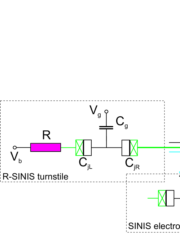
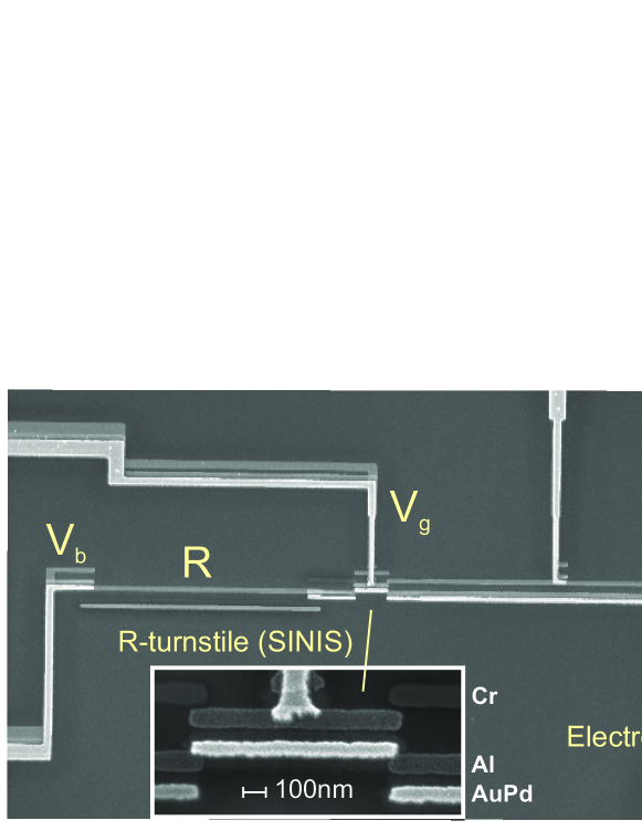
The experimental circuit is shown in Fig. 1. It includes a hybrid SINIS-type R-turnstile, terminated by the trapping island capacitively coupled to a SINIS SET electrometer. An SEM image of the structure is shown in Fig. 2. It was fabricated on the thermally oxidized Si substrate by means of the standard shadow evaporation technique [22]. The layout consists of three replicas of different materials: Cr for the resistor, -thick, evaporated in oxygen at a pressure of about ; Al () oxidized just after the evaporation at for to form the tunnel barrier; and a proximity bilayer of Al () and AuPd (), building together the normal-state island of the turnstile. Here, the thin Al film was used in order to improve the quality of the tunnel barrier. For the purpose of increasing the yield of the intact junctions, the layout included a semiconducting ring of evaporated Si (not shown), cross-connecting all on-chip lines during sample manipulations at room temperature [23].
The trapping island was made of solely the superconducting Al, to avoid unpaired electron states within the energy gap . The island was coupled to the electrometer indirectly through its capacitive link to the neighboring normal-conducting replica, connected galvanically to a spacer electrode, as shown in Fig. 2. Due to the indirect way of coupling, the electrometer response function was sufficiently weak to avoid the back influence of this charge detector onto the trap (see below).
-
Sample No. 1 600 750 260 85 44 25.0 2 120 360 230 38 36 2.6
The measurements were carried out in a dilution fridge with a base temperature of . The sample was encapsulated into a microwave-tight, but not a vacuum-sealed sample holder. Thermocoax coaxial filters, approximately -long, were installed into the sample-holder for every signal line. One exception was, however, made for the high-frequency gate line (used in the present experiment to apply a dc-voltage ), equipped with a much shorter coaxial filter, about .
The results of this paper are demonstrated on two samples with substantially different parameters, determined with the help of relevant test devices and summarized in Table 1. We note that, due to high oxygen content, our resistive Cr lines exhibited slightly non-linear -curves, characterized by the different zero-bias and asymptotic resistances .
3 Results and discussion
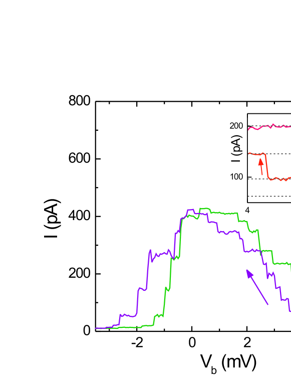
An important manifestation of the trapping effect is a hysteresis, appearing in the charge detector response, as we reverse the direction of charging the trap, see Fig. 3. A single-electron trapping induced a small polarization charge on the electrometer island, corresponding to a th part of the modulation period, as shown in part by a step-like modulation function in Fig. 3. During the voltage sweep in Fig. 3, we applied a cross-talk cancellation signal to the gate , which was used to counterbalance the continuous voltage modulation of the trapping island and the electrometer island. As a result, the discrete detector signal was observed, due to electron tunneling events only, as manifested in the inset to Fig. 3 by a stepped shape of the hysteresis loops.
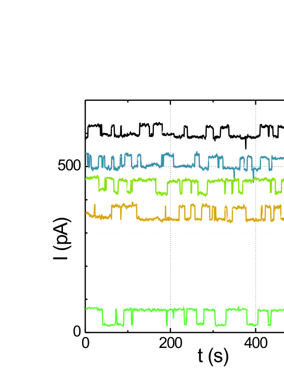
As previously mentioned, the detection of incremental charging of the trapping island was done by means of a voltage-biased SINIS transistor. In order to obtain a measurable output current, the bias voltage was increased above the gap value, , which is sufficiently high to enable appreciable quasiparticle current. Accordingly, one could expect significant disturbances, imposed on the trap by the quasiparticle recombination processes in such a detector. However, as shown in Fig. 4, the frequency of random switchings in the trap was not noticeably affected within the practical range of the electrometer currents, .
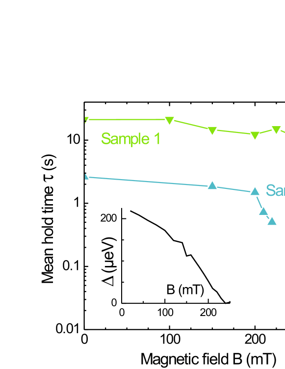
Since, depending on the voltage settings, both one-electron and two-electron (Andreev reflections) tunneling events can, in principle, contribute to the detector signal, we first calibrated the experimental circuit, by driving the sample into the normal state and monitoring the single-electron switchings. In Fig. 5 the dependence is shown of the average hold time on the magnetic field , arranged perpendicular to the substrate. The inset illustrates a suppression of the energy gap with increasing values of . The comparison with the normal-state behavior brought us to the conclusion that the majority of events were related to 1e-tunneling even in the superconducting state. Rare 2e-events were also observed, but they were statistically indistinguishable from a possible small amount of time-unresolved two-electron tunneling sequences. On the other hand, theoretically, a single-electron escape through the SINIS turnstile must leave behind a quasiparticle excitation in the trapping island. This process is, however, prohibited energetically at low bias voltage and low temperatures. Therefore, observation of predominantly single-electron events in our experiment must be attributed to the dominance of non-equilibrium carriers in the escape processes.
The average hold times of two equally populated neighboring charge states were registered to be at the level of , in the high- energy Sample 1, and , in the moderate- Sample 2. These values are remarkable, because such long hold times have been previously observed only for single-electron arrays without resistors with the number of junctions (see Refs. [24, 25, 26]).
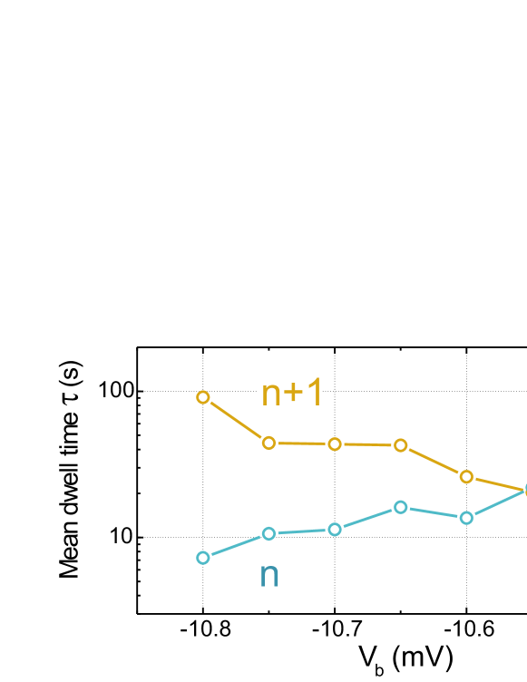
Due to the gate modulation by the cancellation signal (see above), a strong systematic variation of the loop width was observed, as we swept over more than loops. However, for the hold times measurements, we focused on the loop of the maximum width, where only a little change to the neighboring loops was observed. On the other hand, due to the same cancellation signal, an effective bias voltage across the R-SINIS-turnstile-part of the circuit, which was zero in the center of the loop , could be directly obtained in experiment as within the same loop. The latter consideration enables a direct estimate of the practical accuracy of the turnstile at finite bias voltage with the help of the data shown in Fig. 6. One can see that for the half of the gap voltage, which typically corresponds to an optimal bias in the center of the pumping plateau [4, 20], the electron leak is still on the scale of one electron per . Accordingly, for the R-turnstile driven by a rectangular signal [10], i. e. flipped quickly between two optimized gate settings, one could expect a leakage-limited accuracy, say, at the pumping frequency , on the metrological level .
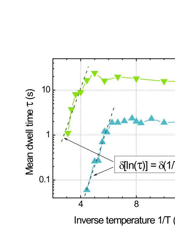
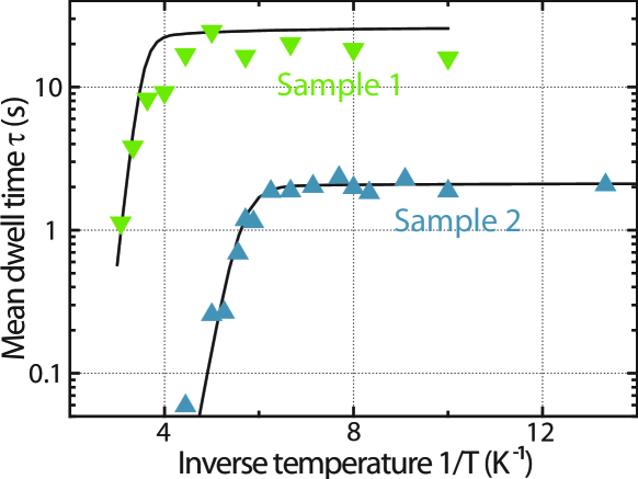
Furthermore, our samples demonstrated no deterioration of the hold time within wide temperature ranges up to (see Fig. 7). This predicts excellent stability against the electron overheating effects for pumping currents up to [27]. At higher temperatures, a fast exponential reduction of the hold times was observed. A slope of the decay, estimated in Fig. 7 to be similar for both samples, reveals a phenomenological activation energy of about , which is considerably lower than in either sample. Our numerical analysis, which we address below, indicates that these deviations from the simple Ahrrenius model of an autonomous SET trap, which basically assumes a strong dependence of on (cf., e.g., Refs. [17, 18]), appears due to the influence of the on-chip resistor and the shape of the BCS density of states in the superconductor.
4 Model of environmental activation of tunneling for the R-SINIS trap
In order to facilitate the understanding of the observed escape processes, we have applied a semi-phenomenological model of environmentally enhanced tunneling in the R-SINIS trap, which assumes that a considerable noise contribution arrives from the warmer parts of the electromagnetic circuitry. Further details related to this Environmental Activation of Tunneling (EAT) approach can be found elsewhere [8, 21].
EAT formalism
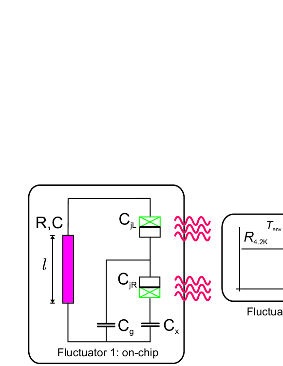
Our modeling of electron escape from the trap is based on the environmental activation of single-particle tunneling events. The theoretical framework is that of standard theory [28], which accounts for the photon exchange with the tunnel junction, due to the excitation of the environmental modes. Our model of the electromagnetic environment of the trap junctions includes two independent fluctuators, as shown symbolically in Fig. 8:
- Fluctuator 1
- Fluctuator 2
-
accounts for the high-frequency noise originating possibly from a source external to the sample stage and having higher temperature. Activation of first-order tunneling by high-temperature environment, , has been previously shown to reproduce the experimentally observed finite sub-gap conductance of NIS junctions [8], and low-temperature saturation of tunneling rates in an NIS single-electron box[21].
In the framework of theory[28], a single-electron tunneling rate is derived on the basis of the absorption/emission spectrum of the environment, the function . For Gaussian fluctuators, can be evaluated as
| (1) |
where is a linear phase-phase correlation function, introduced in Ref. [28] to describe fluctuations of voltage across the tunnel junction. In the case of a linear environment in thermal equilibrium, which can be characterized by an impedance , connected in parallel to the junction of capacitance , equals
| (2) |
where is the total impedance seen over the junction and is the inverse temperature of the environment. In order to describe the experimental setup, we will generalize the above result to the two-fluctuator model, where the voltage fluctuations caused by the independent fluctuators are additive. Consequently, the total function can be found as a convolution
| (3) |
of the partial functions, evaluated independently for the two components (cf., e. g., Ref. [31]).
For a description of filtering and voltage division effects, we allow for an arbitrary transfer function , which relates the fluctuating current through the impedance to the voltage across the junction, so that . The actual phase fluctuations across the junction will then be equivalent to those across an effective total impedance
| (4) |
which can be used for calculations of the function with the help of equations 1,2.
Fluctuator 1: On-chip resistor
-
Sample 1 5 85a 320 40 30 100 24 0.58 0.29 2 5 38 320 100 30 100 44 0.44 0.28 -
aZero-bias resistance was used instead of the asymptotic value .
For evaluating corresponding to the on-chip resistor, we will use the reduced circuit diagram, shown in detail in the left-hand part of Fig. 8. and denote the total capacitance of the Cr wire, and and where is the wire length. For , we take a rule-of-thumb value accounting for geometric stray capacitance. We have introduced a shorthand notation for impedance calculations. The essential transmission line parameters are the frequency dependent wave number, , and the characteristic line impedance, . For a semi-infinite line, the impedance seen from the open end equals the characteristic impedance, and for a finite wire terminated with a short circuit, one finds .
Next, we note that the electrical circuit in parallel to the resistor consists of purely capacitive elements only. Hence, it can be modeled by a single lumped capacitor of value . The voltage fluctuations over the junctions and are equivalent to the fluctuations over , scaled by a factor accounting for the capacitive voltage division. For the left (upper) junction, we have , and for the right, . According to Equation (4), voltage division by factor is equivalent to scaling by a factor of . Based on the preceding argument, we can now write the effective impedance, used for evaluating the function related to Fluctuator 1, as
| (5) |
The numerical values of the model parameters are presented in Table 2.
Fluctuator 2: A source of high-frequency noise
The principal escape mechanism is assumed to be related to the excitation of quasiparticles by the photons with energy , which is high enough to overcome the Coulomb blockade in the turnstile. For both studied samples , and hence the relevant noise frequencies are above . The photon excitations are expected to arrive from the warmer (and more distant) parts of the environment, to be modeled as Fluctuator 2, shown symbolically in the right-hand part of Fig. 8.
Due to the lack of microscopic understanding, we will model Fluctuator 2 just as a parallel circuit at (see previous work in Refs. [8, 21]), coupled directly to either junction. Used as a model parameter, the cut-off frequency of this effective circuit can be reasonably interpreted as the cut-off of the coupling between the source and the junction. Taking into account that the gate capacitances in the reported turnstiles are comparable to those of the (very small) tunnel junctions, we assume the gate lines are the dominant on-chip propagation ways for the external noise. (For simplicity, this concern was disregarded in Fig. 8.) On the contrary, the high-frequency power attenuation for the on-chip Cr resistors is very strong: if modeled as transmission lines, it takes the exponential form with the cut-off frequency .
As long as the hold time at low temperatures depends mainly on the spectral density of environmental emission at high frequencies , the source resistance and cutoff frequency of the high-temperature environment cannot be independently extracted from the measurements. In the calculations, a constant cut-off frequency was used, corresponding to the filtering properties of the Thermocoax lines. We stress that the effective source resistance , obtained as a model fit parameter, formally includes the details of a phenomenological transfer function and is not expected to be equal to the actual source resistance.
Results
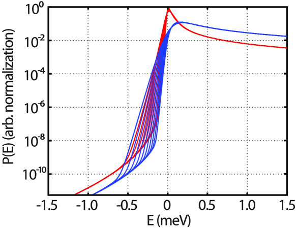
The typical composite functions, resulting from the calculations described above, are shown in Fig. 9. The slowly decaying environmental absorption spectrum () is due to the on-chip resistor, whereas the finite emission probabilities on the millivolt scale at low temperatures stem from the high-frequency noise. A maximum of the functions occurs at a positive voltage due to the dynamic Coulomb blockade arising owing to the on-chip resistor.
The single-electron tunneling rates were computed using the golden rule formula
| (6) |
where is the junction resistance, the density of states in the S electrode, and the occupation factor for quasiparticle states in the N(S) electrode. In our model, we use the pure BCS density of states and the occupation factors are taken to obey equilibrium Fermi distribution, i. e., , where is the sample stage temperature. The assumption of the equilibrium quasiparticle distribution in the S electrodes is based on the ultra low injection rates (of the order of ), allowing for sufficiency of the quasiparticle relaxation/recombination rates on both sides of the turnstile. The tunneling rates were evaluated independently for the left and right tunnel junctions, respectively.
Finally, the hold times were calculated based on the master equation [1] for single-electron tunneling
| (7) |
We note that the sequences, where an electron tunnels to the turnstile island and then back, are too fast to be detected, and hence they do not affect the observed hold times. Furthermore, the charging energy of the trapping node is considered to be compensated in the experiment by an appropriate bias voltage , and it was not included in the simulations.
-
Sample 1 600 260 600 11.3 2 120 230 360 1.8
Figure 10 demonstrates a reasonable agreement of the measured and calculated hold times in the trap. The parameters used in numerical calculations are summarized in Table 3. The fit value of in Sample 1 is lower than its experimental estimate , which we attribute to an effect of a not quite optimum gate voltage setting in measurements. The fit value of for Sample 1 was found larger than that of Sample 2 by a factor of 6.3, corresponding to a factor of in the voltage fluctuation amplitude. Larger voltage fluctuations can be, at least partially, attributed to the lower junction capacitance of Sample 1 compared to Sample 2 (see Table 2). Furthermore, since the photon energy required to overcome the Coulomb blockade barrier is different for the two samples, any deviation of the true noise spectrum from the assumed first-order decay could also result in different fit values for .
At higher temperatures, the hold times are influenced by the thermal broadening of the Fermi-factors, but also by an increased probability of photon emission by the on-chip resistor (see the plot vs. for in Fig. 9). For Sample 1, we evaluated the hold time also in the case of a magnetically suppressed energy gap . The obtained value of is to the order of magnitude consistent with the experimental hold time (see Fig. 5), which provides one more proof of validity for our model.
5 Conclusions and outlook
Our study of the hold times in the two-junction hybrid R-traps gives rise to a promising prediction of the leakage-limited pumping accuracy of hybrid R-turnstiles. The hold times on the scale of up to tens of seconds imply that the metrological accuracy is feasible and could, in principle, be realized with the help of a special rectangular drive [10]. A more detailed study is under way to characterize the leak in the gate-open state of the turnstile, which is relevant to a more common sinusoidal driving signal. The experimental switchings have been successfully interpreted in terms of the environmentally-induced escape processes. In particular, a good agreement has been achieved in the frame of a two-component model of the environment. Significant disturbances have been shown to arrive from the warmer parts of the set-up, supposedly from outside the sample stage. In this respect, an important further insight can be provided by comparing the hold times of the same trapping device, measured in different measurement setups or by varying the quality of noise filtering.
Acknowledgements
Fruitful discussions with S Kafanov and V Bubanja are gratefully acknowledged. Technological support from T Weimann and V Rogalya is appreciated. The research conducted within the EU project SCOPE received funding from the European Community’s Seventh Framework Programme under Grant Agreement No. 218783.
References
References
- [1] Averin D V and Likharev K K 1991 Mesoscopic Phenomena in Solids (Amsterdam: Elsevier) pp 173-271
- [2] Geerligs L J, Anderegg V F, Holweg P A M, Mooij J E, Pothier H, Esteve D, Urbina C and Devoret M H 1990 Phys. Rev. Lett. 64 2691
- [3] Pothier H, Lafarge P, Orfila P F, Urbina C, Esteve D and Devoret M H 1991 Physica B 169 573 Pothier H, Lafarge P, Urbina C, Esteve D and Devoret M H 1992 Europhys Lett 17 249
- [4] Pekola J P, Vartiainen J J, Möttönen M, Saira O-P, Meschke M and Averin D V 2008 Nature Physics 4 120
- [5] Averin D V and Odintsov A A 1989 Phys Lett A 140 251 Averin D V and Nazarov Yu V 1990 Phys Rev Lett 65 2446
- [6] Averin D V and Pekola J P 2008 Phys Rev Lett 101 066801
- [7] Kautz R L, Keller M W and Martinis J M 2000 Phys Rev B 62 15888
- [8] Pekola J P, Maisi V F, Kafanov S, Chekurov N, Kemppinen A, Pashkin Yu A, Saira O-P, Möttönen M and Tsai J S 2010 Phys Rev Lett 105 026803
- [9] Keller M W, Eichenberger A L, Martinis J M and Zimmerman N M 1999 Science 285 1706
- [10] Kemppinen A, Kafanov S, Pashkin Yu A, Tsai J S, Averin D V and Pekola J P 2009 Appl Phys Lett 94 172108
- [11] Maisi V F, Pashkin Yu A, Kafanov S, Tsai J S and Pekola J P 2009 New J Phys 11 113057
- [12] Odintsov A A, Bubanja V and Schön G 1992 Phys Rev B 46 6875
- [13] Golubev D S and Zaikin A D 1992 Phys Lett A 169 475
- [14] Zorin A B, Lotkhov S V, Zangerle H and Niemeyer J 2000 J Appl Phys 88 2665
- [15] Lotkhov S V, Zangerle H, Zorin A B, Niemeyer J 1999 Appl Phys Lett 75 2665
- [16] Lotkhov S V, Bogoslovsky S A, Zorin A B and Niemeyer J 2001 Appl Phys Lett 78 946
- [17] Dresselhaus P D, Ji L, Han S, Lukens J E and Likharev K K 1994 Phys Rev Lett 72 3226
- [18] Krupenin V A, Lotkhov S V and Presnov D E 1997 J Exp Theor Phys 84 190
- [19] Dynes R C, Garno J P, Hertel G B and Orlando T P 1984 Phys Rev Lett 53 2437
- [20] Lotkhov S V, Kemppinen A, Kafanov S, Pekola J P and Zorin A B 2009 Appl Phys Lett 95 112507
- [21] Saira O-P, Möttönen M, Maisi V F and Pekola J P 2010 arXiv:1006 0479 submitted for publication
- [22] Dolan G J 1977 Appl Phys Lett 31 337 Niemeyer J 1974 PTB-Mitt 84 251
- [23] Lotkhov S V, Camarota B, Scherer H, Weimann T, Hinze P and Zorin A B 2009 Proc. IEEE Nanotechnology Materials and Device Conf. (Traverse City, USA) pp 23-26
- [24] Fulton T A, Gammel P L and Dunkleberger L N 1991 Phys Rev Lett 67 3148
- [25] Lafarge P, Joyez P, Pothier H, Cleland A, Holst T, Esteve D, Urbina C and Devoret M H 1992 C R Acad. Sci. Paris 314 883
- [26] Martinis J M, Nahum M and Jensen H D 1994 Phys Rev Lett 72 904
- [27] Maibaum F, Lotkhov S V and Zorin A B 2010 in preparation
- [28] Ingold G L and Nazarov Yu V 1992 Single Charge Tunneling, Coulomb Blockade Phenomena in Nanostructures (NATO ASI Series B vol 294)(New York: Plenum Press) ch 2
- [29] Farhangfar Sh, Toppari J J, Pashkin Yu A, Manninen A J and Pekola J P 1998 Europhys Lett 43 59
- [30] Farhangfar Sh, Manninen A J and Pekola J P 2000 Europhys Lett 49 237
- [31] Ingold G-L, Grabert H and Eberhardt U 1994 Phys Rev B 50 395