Compensation-dependence of magnetic and electrical properties in GaMnP
Abstract
We demonstrate the control of the hole concentration in Ga1-xMnxP over a wide range by introducing compensating vacancies. The resulting evolution of the Curie temperature from to is remarkably similar to that observed in Ga1-xMnxAs despite the dramatically different character of hole transport between the two material systems. The highly localized nature of holes in Ga1-xMnxP is reflected in the accompanying increase in resistivity by many orders of magnitude. Based on variable-temperature resistivity data we present a general picture for hole conduction in which variable-range hopping is the dominant transport mechanism in the presence of compensation.
pacs:
75.50.Pp, 72.80.Ey, 72.60.+gDilute magnetic semiconductors (DMSs), where a few atomic percent of magnetic ions are randomly substituted for a semiconductor host species, represent a remarkable workbench for the study and demonstration of spintronic functionalities.(Dietl et al., 2008) They are not only a means to an end but very exciting materials in their own right, exhibiting many striking phenomena whose interpretation and modeling are extremely challenging – from the ferromagnetic exchange itself to the large anomalous Hall effect.(Jungwirth et al., 2006) Much research has focused on III-Mn-V systems,(Jungwirth et al., 2006; Matsukura, Ohno, and Dietl, 2002; Burch, Awschalom, and Basov, 2008; Sato et al., 2010) where Mn acts as the source of both magnetic moment and carriers that mediate long-range ordering. While the behavior of Ga1-xMnxAs is reasonably well understood at this point, the models developed in the process fall short of describing some other DMSs.(Jungwirth et al., 2006)
Ga1-xMnxP is a prime candidate for further study, due to both its chemical similarity to Ga1-xMnxAs as well as its low lattice mismatch with Si. Because the Mn acceptor level lies approximately four times deeper within the gap with respect to the valence band than in GaAs,(Clerjaud, 1985) the holes are of a much more localized nature. Still, hole-mediated ferromagnetism (FM) has been demonstrated conclusively in Ga1-xMnxP fabricated by ion implantation and pulsed-laser melting (II-PLM).(Scarpulla et al., 2005) In the best samples to date FM signatures persist up to a Curie temperature () of ,(Farshchi et al., 2006) which is lower than for Ga1-xMnxAs at the same .(Jungwirth et al., 2005)
One of the hallmarks of carrier-mediated FM is the dependence of the characteristic electrical, magnetic and optical properties on and carrier (i.e., hole) concentration, . A major line of study pursued has thus been the behavior of Ga1-xMnxP over a range of .(Stone et al., 2006; Farshchi et al., 2006) While these samples implicitly exhibit different as well, this approach only explores part of the available parameter space. Research into samples with constant and varying has been comparatively limited, focusing on anisotropy in S-codoped samples(Stone et al., 2008a) and on in S- and Te-codoped samples.(Scarpulla et al., 2008, 2005)
In this letter we present the first systematic study on the electrical and magnetic effects of hole compensation in Ga1-xMnxP. We utilize the amphoteric nature of native defects (Walukiewicz, 1989) – donor-like in Ga1-xMnxP (Walukiewicz, 1988; Clerjaud, 1985) – to investigate a very wide range of without significantly changing . A similar method has recently been applied to Ga1-xMnxAs,(Mayer et al., 2010) and we find surprising similarities between the materials despite the radically different degree of hole localization. Furthermore, we present a picture for hole conduction by variable-range hopping (VRH) in Ga1-xMnxP.
The samples for this study were prepared by II-PLM.(Scarpulla et al., 2003) A GaP wafer – doped n-type; – was implanted with at an energy of and an angle of incidence of to a dose of . Samples with approximate side lengths of were cleaved along directions and individually irradiated with a single KrF laser pulse ( , ), homogenized to a spatial uniformity of by a crossed-cylindrical lens homogenizer. They were subsequently subjected to HCl etching to remove residual surface damage. These parameters have been used previously to produce samples with .(Farshchi et al., 2006) For our samples, is defined as the peak substitutional manganese () fraction – occurring between and nm below the surface – as determined by a combination of secondary ion mass spectrometry (SIMS) and ion beam analysis (IBA).(Stone et al., 2010) Compensating defects were then introduced into samples by consecutive irradiations with at an energy of and an angle of incidence of , which according to simulations (Ziegler, Ziegler, and Biersack, 2008) yield a vacancy depth profile similar to the typical Mn distribution.
The characterization of several identically prepared Ga1-xMnxP samples was carried out by SQUID magnetometry. All measurements were conducted in zero-field cooled conditions along the in-plane magnetic easy axis,(Bihler et al., 2007) and the diamagnetic background was removed by linear fitting of variable-field magnetic moment data up to at . They revealed an average saturation moment per of in agreement with previous values.(Scarpulla et al., 2005) Temperature-dependent magnetic moment data at revealed , which is well in line with both previous experimental (Farshchi et al., 2006) and theoretical (Katayama-Yoshida et al., 2007) results. Variable-temperature sheet resistance measurements showed similar agreement between samples.
To confirm their structural integrity, samples were characterized after various irradiation doses. Using IBA, we found that the sheet concentration of , , remains constant within experimental errors and by SIMS that the Mn distribution is unaffected. High-resolution transmission electron microscopy and atomic force microscopy similarly show no qualitative changes with ion irradiation. Notably, even the sample with the highest irradiation dose shows no traces of secondary phases.
In order to track the degree of compensation, control samples were processed in parallel by implanting – a hydrogenic acceptor in GaP – to a dose of . On these, direct measurement of the hole concentration as a function of irradiation dose is possible using the Hall effect. From this data we have determined a hole removal rate of holes per , or holes per vacancy when taking into account the simulations. Using this information, we calculate the relative sheet hole concentration , defined as the difference in the sheet hole concentration between the unirradiated reference and the irradiated sample.

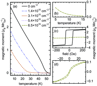
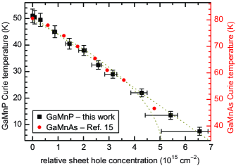
In Fig. 1(a-b) we show for various , revealing a monotonic decrease of with . Similarly, we observe a decrease of with dose as evidenced in Fig. 1(c), consistent with previous studies of donor- or vacancy doping.(Stone et al., 2008a; Mayer et al., 2010) We point out that this is in contrast to being unaffected by hydrogenation,(Bihler et al., 2008; Goennenwein et al., 2004) indicating different mechanisms being involved in passivation versus compensation. The dependence of on is presented in Fig. 2, revealing a virtually linear decline with decreasing hole concentration. We note that the highest irradiation dose of should be sufficient to fully compensate the Mn acceptors, present at . However, as apparent from Fig. 1(a-d), the films are FM at all irradiation doses, implying that they remain p-type even for the highest doses. This apparent discrepancy is explained by the amphoteric defect model (ADM),(Walukiewicz, 1989, 1988) wherein the defect formation energy strongly depends on the Fermi level , resulting in a saturation of the defect doping-induced shift in at a material-dependent stabilization level . This effect becomes dominant in our system for , considerations that are reflected in the error bars where appropriate. Furthermore, the persistence of FM even at these high levels of compensation demonstrates again that the compensation level of as-fabricated films must be very low.(Stone et al., 2010)

Accounting for the ADM-related compensation effects, we observe the relation with for Ga1-xMnxP. Remarkably, such dependence of on is nearly identical to that observed in Ga0.955Mn0.045As (Mayer et al., 2010) films grown by low-temperature molecular beam epitaxy – that is, the trend is identical, barring a certain offset, reminiscent of the similarity in .(Stone et al., 2008b) While our is in a similar range as a p-d Zener model prediction for Ga1-xMnxAs of ,(Nishitani et al., 2010; Dietl, Ohno, and Matsukura, 2001) the model assumption of uniformly distributed delocalized or weakly localized holes does not apply to the Ga1-xMnxP films in this study.
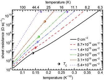
for Ga1-xMnxP samples with varying levels of compensation is displayed in Fig. 3. Films become orders of magnitude more resistive with increasing irradiation dose.

The generally applied, phenomenological model in Ga1-xMnxP has been .(Scarpulla et al., 2005) Here the first term is attributed to thermally activated hole transport via the valence band and the second term to hopping conduction, previously assumed to take place between nearest neighbors.(Scarpulla et al., 2008; Kaminski and Das Sarma, 2003; Shklovskii and Efros, 1984) This model reproduces the behavior of samples with varying which have not been intentionally compensated.(Farshchi et al., 2006) For the current case of compensated films, however, we find overall better agreement with activated transport of the form with a temperature exponent of , separated into a high- and a low-temperature regime characterized by different activation energies . We attribute the general behavior to hopping conduction, specifically VRH.(Shklovskii and Efros, 1984) That this mechanism should dominate even at high for large is reasonable as the energetic difference between delocalized states and – here on the order of the Mn acceptor level of (Clerjaud, 1985) – can easily be an order of magnitude larger than . At , VRH is insufficient to describe fully the transport at high . In this regime, the conduction by holes excited thermally to delocalized states, as described previously,(Scarpulla et al., 2005) contributes or even dominates. This behavior is qualitatively similar to that observed in insulating, low-doped Ga1-xMnxAs (Sheu et al., 2007) and even more so to that in insulating, Sn-codoped Ga1-xMnxAs.(Satoh et al., 2001)
In conclusion, the orders-of-magnitude changes in conductivity and the much more subtle changes in the magnetic response upon compensation using -induced native defects demonstrate the stability of the hole-mediated FM phase in Ga1-xMnxP. While the electrical behavior of Ga1-xMnxP and Ga1-xMnxAs at comparable is dramatically different, these materials display a remarkably similar dependence on both hole concentration and Mn content. This indicates similar mechanisms for inter-Mn exchange in the two systems and places carrier-mediated FM on a continuum of carrier localization in III-Mn-V DMSs.
Acknowledgements.
The work at Berkeley (sample synthesis, electrical and magnetic characterization, ion beam analysis) was supported by the Director, Office of Science, Office of Basic Energy Sciences, Division of Materials Sciences and Engineering, of the U.S. Department of Energy under Contract No. DE-AC02-05CH11231. The work at Linz (structural characterization) was supported by the European Research Council through the FunDMS Advanced Grant within the “Ideas” 7th Framework Programme of the EC, and by the Austrian Fonds zur Förderung der wissenschaftlichen Forschung – FWF (Grants P22477, P20065, and N107-NAN). We thank R. Jakieła for SIMS measurements. P.R. S. acknowledges support from an NSF fellowship, T.E. W. from a Marshall Plan Scholarship.References
- Dietl et al. (2008) T. Dietl, D. D. Awschalom, M. Kamińska, and H. Ohno, Spintronics, edited by E. R. Weber, Semiconductors and Semimetals, Vol. 82 (Elsevier, Amsterdam, 2008).
- Jungwirth et al. (2006) T. Jungwirth, J. Sinova, J. Mašek, J. Kučera, and A. H. MacDonald, Rev. Mod. Phys. 78, 809 (2006).
- Matsukura, Ohno, and Dietl (2002) F. Matsukura, H. Ohno, and T. Dietl, in Handbook of Magnetic Materials, Vol. 14, edited by K. H. J. Buschow (Elsevier, Amsterdam, 2002) pp. 1–87.
- Burch, Awschalom, and Basov (2008) K. S. Burch, D. D. Awschalom, and D. N. Basov, J. Magn. Magn. Mater. 320, 3207 (2008).
- Sato et al. (2010) K. Sato, L. Bergqvist, J. Kudrnovský, P. H. Dederichs, O. Eriksson, I. Turek, B. Sanyal, G. Bouzerar, H. Katayama-Yoshida, V. A. Dinh, T. Fukushima, H. Kizaki, and R. Zeller, Rev. Mod. Phys. 82, 1633 (2010).
- Clerjaud (1985) B. Clerjaud, J. Phys. C 18, 3615 (1985).
- Scarpulla et al. (2005) M. A. Scarpulla, B. L. Cardozo, R. Farshchi, W. M. Hlaing Oo, M. D. McCluskey, K. M. Yu, and O. D. Dubon, Phys. Rev. Lett. 95, 207204 (2005).
- Farshchi et al. (2006) R. Farshchi, M. A. Scarpulla, P. R. Stone, K. M. Yu, I. D. Sharp, J. W. Beeman, H. H. Silvestri, L. A. Reichertz, E. E. Haller, and O. D. Dubon, Solid State Commun. 140, 443 (2006).
- Jungwirth et al. (2005) T. Jungwirth, K. Y. Wang, J. Mašek, K. W. Edmonds, J. König, J. Sinova, M. Polini, N. A. Goncharuk, A. H. MacDonald, M. Sawicki, A. W. Rushforth, R. P. Campion, L. X. Zhao, C. T. Foxon, and B. L. Gallagher, Phys. Rev. B 72, 165204 (2005).
- Stone et al. (2006) P. R. Stone, M. A. Scarpulla, R. Farshchi, I. D. Sharp, E. E. Haller, O. D. Dubon, K. M. Yu, J. W. Beeman, E. Arenholz, J. D. Denlinger, and H. Ohldag, Appl. Phys. Lett. 89, 012504 (2006).
- Stone et al. (2008a) P. R. Stone, C. Bihler, M. Kraus, M. A. Scarpulla, J. W. Beeman, K. M. Yu, M. S. Brandt, and O. D. Dubon, Phys. Rev. B 78, 214421 (2008a).
- Scarpulla et al. (2008) M. A. Scarpulla, P. R. Stone, I. D. Sharp, E. E. Haller, O. D. Dubon, J. W. Beeman, and K. M. Yu, J. Appl. Phys. 103, 123906 (2008).
- Walukiewicz (1989) W. Walukiewicz, Appl. Phys. Lett. 54, 2094 (1989).
- Walukiewicz (1988) W. Walukiewicz, Phys. Rev. B 37, 4760 (1988).
- Mayer et al. (2010) M. A. Mayer, P. R. Stone, N. Miller, H. M. Smith, O. D. Dubon, E. E. Haller, K. M. Yu, W. Walukiewicz, X. Liu, and J. K. Furdyna, Phys. Rev. B 81, 045205 (2010).
- Scarpulla et al. (2003) M. A. Scarpulla, O. D. Dubon, K. M. Yu, O. Monteiro, M. R. Pillai, M. J. Aziz, and M. C. Ridgway, Appl. Phys. Lett. 82, 1251 (2003).
- Stone et al. (2010) P. R. Stone, M. A. Scarpulla, K. M. Yu, and O. D. Dubon, in Handbook of Spintronic Semiconductors, edited by W. M. Chen and I. A. Buyanova (Pan Stanford Publishing, Singapore, 2010).
- Ziegler, Ziegler, and Biersack (2008) J. F. Ziegler, M. D. Ziegler, and J. P. Biersack, “SRIM 2008.04,” http://www.srim.org/ (2008).
- Bihler et al. (2007) C. Bihler, M. Kraus, H. Huebl, M. S. Brandt, S. T. B. Goennenwein, M. Opel, M. A. Scarpulla, P. R. Stone, R. Farshchi, and O. D. Dubon, Phys. Rev. B 75, 214419 (2007).
- Katayama-Yoshida et al. (2007) H. Katayama-Yoshida, K. Sato, T. Fukushima, M. Toyoda, H. Kizaki, V. A. Dinh, and P. H. Dederichs, Phys. Status Solidi A 204, 15 (2007).
- Note (1) See supplementary material at [URL will be inserted by AIP] for SIMS and IBA data.
- Bihler et al. (2008) C. Bihler, M. Kraus, M. S. Brandt, S. T. B. Goennenwein, M. Opel, M. A. Scarpulla, R. Farshchi, D. M. Estrada, and O. D. Dubon, Journal of Applied Physics 104, 013908 (2008).
- Goennenwein et al. (2004) S. T. B. Goennenwein, T. A. Wassner, H. Huebl, M. S. Brandt, J. B. Philipp, M. Opel, R. Gross, A. Koeder, W. Schoch, and A. Waag, Phys. Rev. Lett. 92, 227202 (2004).
- Stone et al. (2008b) P. R. Stone, K. Alberi, S. K. Z. Tardif, J. W. Beeman, K. M. Yu, W. Walukiewicz, and O. D. Dubon, Phys. Rev. Lett. 101, 087203 (2008b).
- Nishitani et al. (2010) Y. Nishitani, D. Chiba, M. Endo, M. Sawicki, F. Matsukura, T. Dietl, and H. Ohno, Phys. Rev. B 81, 045208 (2010).
- Dietl, Ohno, and Matsukura (2001) T. Dietl, H. Ohno, and F. Matsukura, Phys. Rev. B 63, 195205 (2001).
- Kaminski and Das Sarma (2003) A. Kaminski and S. Das Sarma, Phys. Rev. B 68, 235210 (2003).
- Shklovskii and Efros (1984) B. I. Shklovskii and A. L. Efros, Electronic Properties of Doped Semiconductors, Solid-State Sciences, Vol. 45 (Springer, Berlin, 1984).
- Sheu et al. (2007) B. L. Sheu, R. C. Myers, J.-M. Tang, N. Samarth, D. D. Awschalom, P. Schiffer, and M. E. Flatté, Phys. Rev. Lett. 99, 227205 (2007).
- Satoh et al. (2001) Y. Satoh, D. Okazawa, A. Nagashima, and J. Yoshino, Physica E 10, 196 (2001).