Plasmon modes of silver nanowire on a silica substrate
Abstract
Plasmon mode in a silver nanowire is theoretically studied when the nanowire is placed on or near a silica substrate. It is found that the substrate has much influence on the plasmon mode. For the nanowire on the substrate, the plasmon (hybrid) mode possesses not only a long propagation length but also an ultrasmall mode area. From the experimental point of view, this cavity-free structure holds a great potential to study a strong coherent interaction between the plasmon mode and single quantum system (for example, quantum dots) embedded in the substrate.
The silver nanowire is a potential solution to key components in future ultra-compact electronic and photonic circuit ozbay ; wireexp2 ; wireexp3 since it can confine the light in nanoscale beyond the diffraction limit. The strong confinement of light in a small area produces strong electric field intensity and dramatically changes the density of state nearby the metal surface. Therefore, the silver nanowire has been suggested to realize strong light-matter interaction, where the nanowire plays as the role of a resonator in cavity quantum electrodynamics (QED). When an optical emitter, e.g., a quantum dot (QD), is placed around the silver nanowire, its spontaneous emission can be significantly modifiedchang1 , known as the Purcell effect. As a result, single optical emitter coupling with plasmon modes of nanowire holds a great potential for broad-band cavity QED chang1 , single photon source akimov , and sub-wavelength single photon transistor chang2 ; chen for quantum information science.
Theoretically, the plasmon mode in silver nanowire was studied as an ideal axis-symmetric mode chang1 , or still treated without the external influence even it was placed on a substrate zma ; yma ; tshegai ; rxyan ; dong . However, in realistic applications, the silver nanowire is always necessary to be located on or near a substrate. For example, the nanowire on a substrate makes it convenient for manipulating assisted by the scanning near field optical microscope probe zma ; yma ; tshegai ; rxyan ; pyayt ; dong ; sanders ; hwei ; baik . To the best of our knowledge, the influence on the plasmon mode from the substrate is still kept un-studied. Actually, the plasmon mode is very sensitive to the surrounding environment. In this Letter, we theoretically study the plasmon mode propagating along the silver nanowire near a substrate with a gap . In this silver-air-substrate structure, most of the mode energy is confined around the interface between the substrate and silver nanowire. It is very different from the nanowire simply embedded in air. The benefit of the nanowire on a substrate is that the large portion of energy in the substrate reduces the mode area by a factor of 5, without significant degradation of the propagation loss.

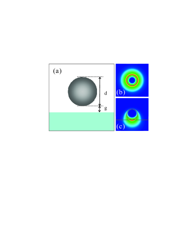
An infinite long silver nanowire with a diameter of is near an infinite dielectric substrate with a gap of . The cross section is shown Fig. 1(a). The surface plasmon mode propagates harmonically along the nanowire, and the electric field varies as , where the propagation constant is a complex number because of the energy attenuation in the propagation. In this case, the Maxwell equation is reduced to two-dimensional cross section, which can be expressed as
| (1) |
where and denote the refractive index of material and the effective index for the mode, respectively. The propagation length of the plasmon modes can be defined as
| (2) |
Besides the propagation loss, another important parameter of the plasmon mode is effective mode area , which can be defined by the ratio of a mode’s total energy density per unit length and its peak energy density,
| (3) |
where represents the effective energy density with
| (4) |
Here, and are the intensity of electric and magnetic fields, respectively. and are the electric and vacuum magnetic permittivities.
To describe the impact from the substrate, we also define the confinement factor as the portion of energy in substrate,
| (5) |
The confinement factor can also quantify the interaction of SPP and substrate,
A finite element method is used to investigate the plasmon modes with a fixed wavelength at nm. The energy distribution profiles of the plasmon modes in the nanowire are shown in Fig. 1(b) and (c), with , respectively. Here, and . It is not difficult to find a rotation symmetric field distribution when the nanowire is in air (), while a strongly asymmetric field distribution is presented in the presence of the silica substrate (). Moreover, the maximum of the electric field is distributed in the substrate-nanowire gap. In other words, the substrate can significantly pull the mode field.

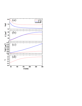
We first investigate the impact of the substrate on the plasmon modes for various nanowire sizes. Fig.2 shows the effective index (), propagation length (), effective mode area () and portion of energy () versus . As a comparison, the ideal case without substrate () is also depicted. It is found that decreases with the increase of , while and shows the opposite behaviors. This tradeoff between confinement and absorption loss is well known in the surface plasmon mode.
For the nanowire on silica substrate, comparing with the nanowire in air, is larger and is smaller with all . These obvious differences come from the presence of large refractive index material near the metal nanowire. In addition, the mode area of the nanowire on silica substrate is only about 1/5 of that in air. To characterize the field pulling by the silica substrate, we present the confinement factor for in Fig.2(d). The increases with to nearly when .
In Fig.(2), simply increases with the increase of . However, the other three parameters approach saturation values. In order to get a physic interpretation, we can approximately treat this hybrid system as the metal plane-substrate for large . The analytical solution to Eq. (1) in the plane condition gives , where and is the electric permittivity of metal and substrate. So we have , , and in the plane limit.
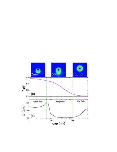
Now, we turn to discuss the experimental condition, where the nanowire is near the substrate with a finite gap . This is a realistic case for many experiments because the substrate is not perfect smooth, or in specific experimental config, the nanowire is suspended in airfalk . By fixing the diameter nm, we study the propagation loss and effective index (Fig.3) for different gaps between nanowire and substrate.
With the increase of gap , monotonously decreases and gradually approaches the in-air case. This is because the influence of substrate becomes smaller when the nanowire departs from the substrate. When nm, the substrate has a very minor effect on the plasmon mode of the silver. However, the dynamics of is much more complicated than that of . When the silver nanowire moves away from the silica substrate, increases first, then quickly drops to . After that, it slowly increases, and finally approaches to m note . We can divide the gap into three regimes: the near field, dissipation, and far field regimes, which correspond to different dynamics of and different loss mechanisms.

(i) Near field regime. In this regime, we have . Due to the phase mismatching, the dominant loss of the plasmon mode comes from the metal absorption. By increasing the gap, gradually decreases as the nanowire moves away from the substrate. A smaller indicates a smaller energy portion in the metal, so that the absorption loss is reduced with increasing .
(ii) Dissipation Regime. When the gap further increases, may be smaller than . Meanwhile, the plasmon mode still has much energy in the substrate, as can be seen in the inset of Fig.3 ( nm). From Eq. (1), when , the solutions are traveling waves in substrate as . The energy in traveling wave will dissipate into infinite space. Therefore, in this regime, the mode energy quickly dissipates by coupling to the dissipative traveling waves in the substrate. As a result, has a sudden decrease.
(iii) The far field regime. When the nanowire further moves away from the substrate, for example, nm, the coupling between the plasmon mode and the dissipative traveling modes in substrate becomes very weak as it is proportional to their field overlap. Thus, even , the plasmon mode keeps almost unchanged by the substrate, and the mode profile approaches the case of (in the absence of the substrate). Therefore, can be slowly recovered in this regime.
The above results indicate that the approximation by neglecting the substrate is not applicable in analyzing experimental results, where the energy confinement and propagation loss are significantly influenced by the substrate. When the gap is very small, most of the energy is confined near nanowire-substrate interface and is large. It should be more efficient to coupling light to the surface plasmon mode through the substrate, especially for large . The efficiently excitation of surface plasmon mode through substrate have been demonstrated recentlytshegai ; rxyan . It is worth noticing that the propagation loss strongly depends on the gap. In a recent experiment, near field surface plasmon mode detection is demonstratedfalk , where the silver nanowire is put on the Ge nanowire, with nm, nm and nm. From Fig. 3(b), it works in the dissipation regime with . For more efficiently detection, should be larger than nm or smaller than nm .
In conclusion, we have numerically studied the mode profile, propagation loss and mode area of plasmon modes of a silver nanowire near the silica substrate. To reduce the propagation loss, our result suggests that the gap between silver nanowire and the substrate should be as small as possible. When the silver nanowire is attached to the substrate (), the propagation length is limited by metal absorption and the mode area is reduced by a factor of . In addition, for nanowire with nm, the field energy portion of the plasmon mode in the substrate is as large as , which is suitable for coupling to QDs or molecules embed in substrate. Accompanying with the scanning near field optical microscope, the silver nanowire can be precisely moved on the substrate, and selectively coupled to single QDs in substrate. This is potential for experimental realization of the single photon transistors, or coupling two distant QDs to generate entanglement for quantum information science.
The work was supported by the National fundamental Research Program of China under Grant No 2006CB921900, the Knowledge Innovation Project of Chinese Academy of Sciences, and National Natural Science Foundation of China (Grant No. 60621064, 60537020). F.W. S. is also supported by the new faculty starting funds from USTC and the Fundamental Research Funds for the Central Universities.
References
- (1) E. Ozbay, Science 311, 189 (2006).
- (2) H. Ditlbacher, A. Hohenau, D. Wagner, U. Kreibig, M. Rogers, F. Hofer, F. R. Aussenegg, And J. R. Krenn, Phys. Rev. Lett. 95, 257403 (2005).
- (3) R. Kolesov, B. Grotz, G. Balasubramanian, R. J. Stohr, A. A. L. Nicolet, P. R. Hemmer, F. Jelezko, and J. Wrochtrup, Nature Phys. 5, 470 (2009).
- (4) D. E. Chang, A. S. Srensen, P. R. Hemmer, and M. D. Lukin, Phys. Rev. Lett. 97, 053002 (2006).
- (5) A. V. Akimov, A. Mukherjee, C. L. Yu, D. E. Chang, A. S. Zibrov, P. R. Hemmer, H. Park and M. D. Lukin, Nature 450, 402 (2007).
- (6) D. E. Chang, A. S. Srensen, E. A. Demler and M. D. Lukin, Nature Phys. 3, 807 (2007).
- (7) W. Chen, G.-Y. Chen, and Y.-N. Chen, Opt. Express 18, 10360-10368 (2010)
- (8) Z. Ma, X. Zhang, X. Guo, Q. Yang, Y. Ma, and L. Tong, Appl. Phys. Lett. 96, 051119 (2010).
- (9) Y. Ma, X. Li, H. Yu, L. Tong, Y. Gu, and G. Gong, Opt. Lett. 35, 1160 (2010).
- (10) T. Shegai, Y. Huang, H. Xu, and M. Käll, Appl. Phys. Lett. 96, 103114 (2010).
- (11) R. X. Yan, P. Pausauskie, J. X. Huang, and P. D. Yang, Proc. Natl. Acad. Sci. U.S.A. 106, 21045 (2009).
- (12) C.-H. Dong, X.-F. Ren, R. Yang, J.-Y. Duan, J.-G. Guan, G.-C. Guo, and G.-P. Guo, App. Phy. Lett. 95, 221009 (2009).
- (13) A. L. Pyayt, B. Wiley, Y. Xia, A. Chen, and L. Dalton, Nat. Nanotechnol. 3, 660 (2008)
- (14) A. W. Sanders, D. A. Routenberg, B. J. Wiley, Y. Xia, E. R. Dufresne, and M. A. Reed, Nano Lett. 6, 1822 (2006).
- (15) J. M. Baik, S. J. Lee, and M. Moskovits, Nano Lett. 8, 642 (2009).
- (16) H. Wei, D. Ratchfor, X. Li, H. Xu, and C.-K. Shih, Nano Lett. 9, 4168 (2009).
- (17) A. L. Falk, F. H. L. Koppens, C. L. Yu, K. Kang, N. D. L. Snapp, A. V. Akimov, M. H. Jo, M. D. Lukin and H. Park, Nature Phys. 5, 475 (2009).
- (18) R. F. Oulton, V. J. Sorger, D. A. Genov, D. F. P. Pile, and X. Zhang, Nature Photon. 2, 496 (2008).
- (19) Similar behavior of SPP have been observed in the case of sliver slab near a substrate, which could be solved analytically.