Mesoscopic transport in ultrathin films of La0.67Ca0.33MnO3
Abstract
We investigate the electrical transport in mesoscopic structures of La0.67Ca0.33MnO3 in the regime of the metal-insulator transition by fabricating microbridges from strained and unstrained thin films. We measure current-voltage characteristics as function of temperature and in high magnetic fields and with varying film thickness. For strained films, in warming from the metallic to the insulating state, we find non-linear effects in the steep part of the transition characterized by a differential resistance with a strong peak around zero applied current, and saturating at higher currents after resistance drops up to 60 . We propose that this nonlinear behavior is associated with melting of the insulating state by injecting charge carriers, signalling the occurrence of an intervening phase which involves the formation of short range polaron correlations.
Doped manganites are strongly correlated electron systems which show a large variety
in physical properties. The material La0.67Ca0.33MnO3(LCMO) for
instance shows a transition from a paramagnetic insulator to a ferromagnetic metal
around = 250 K and the well known colossal magnetoresistance (CMR) effect.
The physics is mainly determined by competing interactions: trapping of the
electrons in Jahn-Teller (JT) distortions (polarons) and the itinerancy of the
electrons in the Double-Exchange mechanism zener4 when spins become
polarized. This competition signals that only small free energy differences exist
between a variety of different possible phases of the system. As a result the phase
of the material can be tuned easily by various external perturbations, such as
magnetic and electric fields, strain and disorder. For instance, the application of
strain amplifies the JT splitting of the eg levels and makes the distortions more
static in nature. This has an inhibiting effect on band formation, which leads to
reduction of TMI in manganite thin films compared to the bulk value
freisem4 ; dorrrev4 . Furthermore, the susceptibility of the M-I transition to
disorder (doping disorder, oxygen nonstoichiometry, defects from strain relaxation,
twinning, and grain boundaries) can lead to the coexistence of the metallic and
insulating phases
on a variety of length scales uehara2 ; lynn5 .
Electrical transport in these correlated electron systems is therefore a complex
phenomenon, which has however hardly been probed on small length scales. Here we
address such transport in the mesoscopic regime, by investigating microbridges made
in LCMO thin films, grown in a strained or unstrained state on SrTiO3 (STO) or
NdGaO3 (NGO) substrates. In the strained films we do find strongly nonlinear
transport behavior in the CMR regime near the metal-insulator transition,
characterized by increased conductance at higher current. We attribute these effects
to the intrinsic physics of the insulating state in terms of the formation of an
intervening glassy polaron state when going from the correlated metal to the
polaronic insulator.
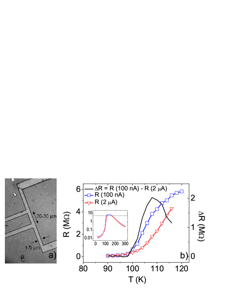
We have grown LCMO thin films with varying thicknesses between 7 - 20 nm on STO and NGO substrates, by DC-sputtering in an oxygen atmosphere of 3 mbar and at a growth temperature of 840∘C. The STO induces a tensile strain in the LCMO film due to the lattice mismatch of -0.6 , the NGO is (almost) lattice matched. After growth, x-ray measurements were performed to check the thickness of the films. Furthermore, Electron Energy Loss Spectroscopy (EELS) was used to characterize the elemental composition and Mn valence state of the samples beekman2 . We find that our films have compositions close to that of the sputtering target and correct oxygen stoichiometry. The films were patterned using electron-beam lithography and conventional Ar-etching followed by an oxygen plasma etch to restore the insulating properties of the substrate beekman . The mesoscopic LCMO structure has a four-point configuration with dimensions of 5 m (width) by 20 - 30 m (length between voltage contacts), as shown in Fig.1a. Macroscopic Au/MoGe contacts were fabricated in a second e-beam step. We measured - curves as function of temperature and in high magnetic fields using a Physical Properties Measurement System (Quantum Design) for temperature control ( = 20 - 300 K) and for magnetic field control ( = 0 - 9 T), but with external current sources and voltmeters.
- characteristics, measured by varying the current, were obtained across the temperature range of 20 - 300 K in order to obtain the differential resistance. All microbridges were also measured in a magnetic field of 5 T to investigate the magnetoresistance (MR) effect. Our main findings are shown in Fig.1b. It shows the resistance vs. temperature () of a microbridge on STO, measured at currents of 100 nA (current density J = 2x10⁶ A/m2) and 2 A (J = 4x10⁷ A/m2). As can be seen in the inset, where is plotted logarithmically, both sets of data show a clear M-I transition typical for strained LCMO thin films with = 130 K (peak temperature) and a resistance drop of three orders of magnitude.

The main panel of Fig.1b shows on a linear scale. The higher current density results in a reduction of resistance just below TMI, which produces a shift in the upper part of the transition of 5 to 10 K. Also shown is the difference between the two curves, which peaks between 105 K and 110 K. If we define a current-induced resistance called Electroresistance (ER() = ), then we observe a maximum ER effect up to 60 for the 10 nm microbridge.
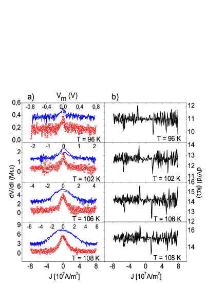
The measured - curves are linear for microbridges on NGO and linear for most temperatures in the case of STO. However, for microbridges on STO we find nonlinear behavior in the steep part of the transition which corresponds to the behavior shown in Fig.1. Typical nonlinear behavior is shown in Fig.2.

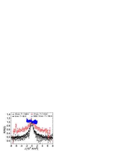
The left panel shows the differential resistance for the 10 nm microbridge at four different temperatures in 0 T as function of applie d current density (bottom axis) and also as function of the measured potential difference (Vm) between the voltage contacts (top axis). At low temperature all - curves are linear up to = 8x10⁷ A/m2 (I = 4 A). Upon warming into the transition the nonlinear behavior starts to occur just below T = 96 K and appears to continue until TMI. For all microbridges the differential resistance is largest at zero bias and drops with increasing applied current density. The full width of the peak appears to increase by more than an order of magnitude from about 2x10⁶ A/m2 (0.2 V) at T = 96 K up to 4x10⁷ A/m2 (8 V) at T = 110 K. However, due to the voltage limit of the nanovoltmeter, it is difficult to observe any nonlinear behavior between 110 K - 170 K. Above this temperature range all - curves are linear. From the right panel it is clear that application of a high magnetic field leads to a reduction in the differential resistance and to complete disappearance of the nonlinearities in the - curves; they are linear across the entire temperature range. To compare the differential resistance behavior of different microbridges we show (, Fig.3), normalized to the value at zero bias, as function of current density for three microbridges on STO with different thicknesses. The film thickness is indicated for each curve as well as the temperature at which the - curve was measured.

The variation in () with becomes less strong when the microbridge thickness is increased. Also shown in Fig.3 are similar data of a 10 nm LCMO film grown on an NGO substrate (TMI = 165 K) measured at 150 K, again in the steep part of the transition. Although measured in a somewhat smaller current density range we find no nonlinear behavior in films on NGO for thicknesses down to 10 nm.
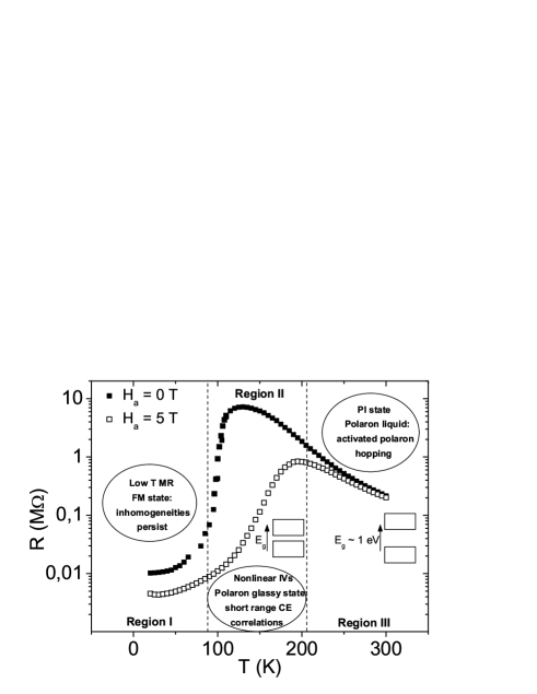
Besides the well known CMR effect in the transition, we also observe a strong MR
effect at low temperatures both for microbridges on STO and on NGO. As becomes clear
from Fig.4a this effect too depends on the microbridge thickness. For the
17 nm thick bridge the curves at 0 T and 5 T almost overlap, but for the 10
nm thick bridge a high magnetic field induces a significant reduction in resistance
at low temperature. The magnitude of the low temperature MR increases with reducing
film thickness reaching about an order of magnitude for the 6.4 nm thick film, see
Fig.4b. Furthermore, also the (unstrained) 10 nm thick film on NGO shows
a MR effect, of 50 at low temperature. Apparently, even for the unstrained LCMO
microbridge an applied magnetic field can result in an increased metallicity at low
temperature. On the other hand, we stress that in this regime of enhanced MR the
- characteristics are simply ohmic.
Behavior as found here under the controlled circumstances of substrate, sample thickness, and bridge width, has not been reported before. Nonlinear behavior was observed recently in thick unstructured and strongly oxygen deficient samples liu5 , but temperature regime, magnetization and field dependence were all different, and it is difficult to connect that work to our observations, in particular since the EELS characterization showed that oxygen deficiency is not an issue in our LCMO films. A concern can be that the observations are an artefact caused by Joule heating in the microbridge. The peak resistivity is around 105-106 cm which we can use to estimate the effect of Joule heating in the measured current density range. The power inserted into the bridge is of the order of W; the estimated Joule heating would be in the mK range which is clearly negligible. Furthermore, heating would lead to different nonlinear behavior, namely increasing resistance with increasing current, and can be ruled out as a possible cause for the observed nonlinearities. Another concern could be the influence of the structural phase transition, tetragonal to cubic, which occurs in the STO substrate at = 105 K . Since our LCMO films are epitaxial this could influence microbridge properties. However, we have shown that the observed nonlinear behavior can occur at different temperatures, both above and below T = 105 K. This indicates that the nonlinear behavior is not an STO-induced effect but intrinsic to the material LCMO.

We conclude from this that the non-linear behavior has to be the
fingerprint of an organized phenomenon intrinsic to the electron
matter formed in the manganite. Next we discuss the different
regimes we believe are present, c.q. the different states of the
microbridge as it is warmed through the metal-insulator
transition. In Fig.5 we provide the R(T) data of the 10
nm microbridge again, in order to help in identifying the various
regimes. At low temperature (region I), the strong MR effects show
that a high magnetic field can still assist in increasing the
metallicity of the microbridge. We believe this to derive from
static inhomogeneities which lead to a relatively high residual
resistance in the thinnest films and locally frustrate the DE-type
metallic state which then forms easier in a (high) magnetic field.
The effect is rather similar to the MR reported in
Ref.eblen05 in thin films of La0.8Ca0.2MnO3
which also exists down to the lowest temperatures.

Upon warming into the transition the conduction electrons become more localized, with the Jahn-Teller splitting of the eg-levels, assisted by the strain in the film, leading to polaron formation. In the steep part of the transition we start to observe strongly nonlinear behavior, and increasing conductance with current. The nonlinearities are fully reversible, indicating that the process which enhances the conductance is not a first-order transition. A scenario in which current transforms a possible antiferromagnetic insulator to a ferromagnetic metal, e.g. through spin torque processes, is not likely, since the closeness of the M-I transition in LCMO to a first-order transition kim5 would probably render this process hysteretic. The scenario we propose instead is that of current-induced melting of an intervening phase which can sustain a voltage difference, while its electrical properties are extraordinarily sensitive to the injection of charge carriers as occurs in the high current state. Such a phase was actually demonstrated to exist, and is called the polaron glass phase lynn5 . We can understand the origin of this phase by remembering that at higher doping of x 0.5, the material is antiferromagnetic and charge and orbital ordered. At lower doping x = 0.33 (our material), this ordering is frustrated, but polaron correlations can still occur. In ref.lynn5 it was shown through neutron scattering experiments that a correlated polaron (glass) phase is formed in LCMO single crystals. The nanoscale structural correlations occur just above TMI. The development of these static (charge ordered, CE-type) polaron structures trap electrons and drive the system into the insulating state. In our case the correlated regions already start to occur below TMI and become more abundant when the bridge is warmed through the transition, a process facilitated by the strain, which causes more disorder on nanoscales as well as larger Jahn-Teller distortions and smaller band-widths. The resulting glass phase fully closes the bridge off. The injection of carriers into this nascent state by applying a chemical potential difference works against the formation of the polaron correlations and drives the system to a different, more metallic, equilibrium. We note that the large CMR effect in the transition is in itself related to the occurrence of the correlated polaron phase, as reported both experimentally kiryukhin5 ; tendeloo5 and theoretically sen5 , while a similar scenario was suggested for the bilayer compound La1.2Sr1.8Mn2O7 mannella5 . Much weaker CMR effects are observed in systems with only single dynamic polarons (large bandwidth materials such as La0.67Sr0.33MnO3). Warming into region III, the polaron correlations break down (polaron liquid) and conduction is governed by thermally activated (single) polaron hopping.
In summary, we find that, upon reducing the size of a strained LCMO film grown on an STO substrate, novel behavior in the transport properties occurs, notably non-linear current-voltage characteristics. This is not found in wider bridges or when strain is absent (films on NGO). As a possible explanation we use the concept of a phase of glassy polarons which is formed in the M-I transition, assisted by the strain, and which is very sensitive to the injection of charge carriers, leading to current-induced melting of the newly forming insulating state.
We thank I. Komissarov for discussions, and M. Porcu and H. Zandbergen for performing the EELS measurements. This work was part of the research program of the Stichting voor Fundamenteel Onderzoek der Materie (FOM), which is financially supported by NWO.
References
- (1) C. Zener, Phys. Rev. 82, 403 (1951).
- (2) J. Aarts et al., Appl. Phys. Lett. 72, 2975 (1998).
- (3) K. Dörr, J. Phys. D: Appl. Phys. 39, R125 (2006).
- (4) M. Uehara et al., Nature 399, 560 (1999).
- (5) J.W. Lynn et al., Phys. Rev. B 76, 014437 (2007); and references therein.
- (6) C. Beekman et al., Phys. Rev. B, in preparation.
- (7) C. Beekman et al., Appl. Phys. Lett. 91, 062101 (2007).
- (8) S.J. Liu et al., J. Appl. Phys. 103, 023917 (2008).
- (9) M. Eblen-Zayas et al., Phys. Rev. Lett. 94,037204 (2005).
- (10) D. Kim et al., Phys. Rev. Lett. 89, 227202 (2002).
- (11) V. Kiryukhin et al., Phys. Rev. B, 70, 214424 (2004).
- (12) V. Moshnyaga et al., Phys. Rev. B 79, 134413 (2009).
- (13) C. Sen et al., Phys. Rev. Lett. 98, 127202 (2007).
- (14) N. Mannella et al., Phys. Rev. B 76, 233102 (2007).