Superconducting junctions from non-superconducting doped CuO2 layers
Abstract
The theoretical approach proposed recently for description of redistribution of electronic charge in multilayered selectively doped systems is modified for a system with finite number of layers. A special attention is payed to the case of a finite heterostructure made of copper-oxide layers which are all non-superconducting (including non-conducting) because of doping levels being beyond the well-known characteristic interval for superconductivity. Specific finite structures and doping configurations are proposed to obtain atomically thin superconducting heterojunctions of different compositions.
pacs:
74.72.-h, 74.78.Fk, 74.25.Jb, 74.45.+cAn interesting area in nanoengineering of materials was opened in a series of experiments by Bozovič et al Boz1 on atomically perfect stacks of selectively doped perovskite layers. These and some other papers Goz1 ; Boz2 mainly used periodic multilayered structures where essential new electronic effects, as interface SC between nominally non-SC layers Boz2 , appeared due to charge redistribution between layers and related shifts of in-plane energy bands. The basic condition for SC to appear within few perovskite layers or even in a single layer is that the local density of hole charge carriers occurs within a definite, rather narrow, interval: with and (carriers per site). The required density distribution results from the corresponding shifts of in-plane energy bands by local Coulomb potentials. A simple theoretical model for such processes was proposed lok , combining a discrete version of Poisson equation for potential with a band-structure modified self-consistent Thomas-Fermi charge density. This approach gives exact solutions for infinite periodical and some other unbounded systems. However recent studies Goz2 ; Smad ; Log showed that pronounced modification of electronic ground state and related SC transitions can be obtained either in stacks of finite (and small) number of layers which is quite promising for practical applications in nanoengineered composite devices. The following consideration aims on an extension of the previous model on an arbitrary layered system and establishing criteria for its optimum SC performance. This line of study can be seen as a practical realization of long envisaged Ginzburg’s program for ultrathin superconducting states ginz .
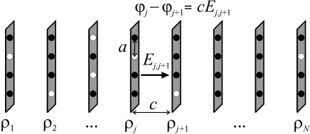
Following the same assumptions as in Ref. lok , we express local charge density in j-th layer: , through the densities of mobile holes and of ionized dopants ( is the elementary charge) and then present the potential difference between neighbor layers as:
| (1) |
This value is obtained considering the electric field in the spacer as the geometric sum of fields emitted by each l-th charged layer: , on both sides of this spacer. Eq. 1 involves the in-plane and c-axis lattice constants and , and is the (static) dielectric constant that effectively reduces the Coulomb field in the c-direction. Eq. 1 would be exact for a stack of mathematical planes, with uniform in-plane charge densities and separation , and it should be a reasonable model for real layers where delocalized holes and localized dopants are distributed in different atomic planes within the period of jth layer. The adopted form of purely dielectric screening is justified in neglect of c-hopping processes, accordingly to their above mentioned weakness, also this model neglects polarization effects from the insulating substrate. We note that the charge densities naturally vanish in uniformly doped (), including undoped (), systems.

Otherwise, the hole carrier density can be related to the local potential using the respective density of states (DOS) :
| (2) |
with the spin factor 2 (this zero-temperature formula is justified for all the considered temperatures ). Thus the role of c-hopping in this model is reduced to establishing the common Fermi level for all the layers. Using the simplest approximation of rectangular DOS: within the bandwidth , we arrive at the linear relation between and :
| (3) |
Then, inserting Eq. 3 into Eq. 1, we obtain the linear relation between carrier and dopant densities, referred to the spacer:
| (4) |
where the dimensionless quantity:
| (5) |
is the single material parameter of the model. Finally, subtracting the relations, Eq. 4, for and spacers leads to simple linear equations for the hole carrier densities in neighbor layers only:
| (6) |
The advantage of Eq. 6 against possible analogous relations between the potentials is in avoiding the need to know the Fermi level position (doping dependent). For an infinite stack of layers, summing these equations in all would automatically assure the total electroneutrality condition , and this was just the way used in Ref. lok to obtain a more detailed alternative to the phenomenological Thomas-Fermi treatment Smad . However, for a finite stack of layers, this condition should be additionally imposed besides the relations, Eq. 4, in order to completely define all the densities . Since Eq. 6 in this case only applies for the internal layers , one needs two more equations which can be obtained from Eq. 4 for terminal layers, and , under the electroneutrality condition:
| (7) |
Thus the non-uniform linear system of Eqs. 6, 7 can be presented in the matrix form as:
| (8) |
where the finite -stack of layers generates the "Laplacian" matrix:
| (9) |
and the -vectors:

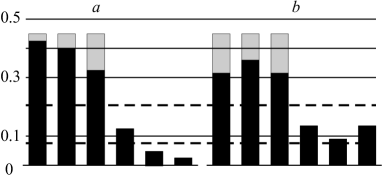
It is seen from Eq. 8 that plays the role of localization parameter: the carrier density strictly coincides with the doping distribution in the limit , otherwise it is spread beyond this distribution, the stronger the smaller is. Generally, the standard solution with the resolvent gives the densities in terms of the doping levels and of the localization parameter as for the instance in Fig. 2 with , (a reliable estimate for real La2CuO4 pog; kast ; chen ) and . It is of interest to compare this solution to that for an unlimited system with the same distribution of dopants but periodically repeated, so that the matrix is replaced by its periodic version:
| (10) |
A notable difference in the resulting distributions of densities is seen in Fig. 2a,b. An important feature of superconducting layers formed in each of these structures (4th layer in Fig. 2a and 4th and 6th layers in Fig. 2b) is that they are realized in nominally undoped La2CuO4 and thus can be expected almost free of undesirable disorder effects (as scattering by defects and consequent fluctuations of the SC order parameter lang ).

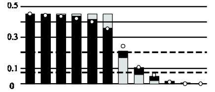
Also a comparison of such calculation with the experiment data Log is presented in Fig. 3, using the real values of structure parameters: and (the three last values are due to the interdiffusion of Sr dopants into nominally undoped La2CuO4 layers), and the same localization parameter as before. The resulting distribution of carrier densities (black columns) displays an excellent coincidence with its measured values. In particular, the carrier density occurs within the SC interval just in the layer with the value that just corresponds to the observed transition temperature K when used in the phenomenological formula lok with K.
From such a good agreement, one expects that this approach can be also used for design of new configurations with tailored superconducting performance. In particular, an interesting possibility is to build ultra-quantum heterojunctions of two types: superconductor- insulator-superconductor (SIS) and superconductor-normal metal-superconductor (SNS), each component being restricted to a single cuprate layer. Such junctions could realize a single layer limit of already discussed thicker SIS and SNS nanostructures with giant proximity effect Boz4 . It should be noted that since the localization parameter value (see Eq. 6) is rather fixed by the choice of the building material (with for La2CuO4), the practical control parameters in this process must be the total number of layers in the stack and particular doping levels in each layer.
Thus, one possible simple structure to produce a SNS junction can consist of cuprate layers with the doping levels defined for instance as: (that is, nominally all non-superconducting). From Eq. 8, the resulting carrier density distribution: , correspond to nomal (overdoped) metal layers, to superconducting layers with a high enough transition temperature K, separated by the layer with and low transition temperature K. Then, in the temperature range one should obtain a SNS heterostructure. If so, the quasiparticle spectrum of this junction will present a peculiar combination of gapped (a kind of size quantization) and gapless branches with interesting IR absorption and electric transport properties.
As to the SIS heterostructure, it is rather difficult to be obtained in the suggested stack, but it can be achieved, e.g., by adding one more undoped layer (i.e., from 3 to 4) to the above structure, or introducing electronic doping in the central layer (making ). Unlike the above SNS case, the resulting SIS junction should display a quasiparticle spectrum with gapped branches only.
In conclusion, an extension of the recent electrostatic model for charge redistribution in non-uniformly doped multilayered systems is proposed for finite (mostly small) number of layers. Formal solutions of this model are mainly analyzed in the parameter range actual for the experimentally investigated multilayers. The distinctions of finite stacks from previously studied unlimited or cyclic systems are indicated. Some new specific arrangements of doped and undoped layers are suggested for realization of artificial atomically thin heterostructures with unusual electronic excitation spectrum, potentially interesting for applications in nanocomputing devices. Such artificial structures may present also an interest for their behavior under applied magnetic field.
This work was partially supported by the Special Program of Fundamental Research of the Department of Physics and Astronomy of NAS of Ukraine. The authors are grateful to I. Bozovič for reading the manuscript and valuable discussion.
References
- (1) I. Bozovič, IEEE Trans. Appl. Superconduct. 11, 2686 (2001).
- (2) A. Gozar, G. Logvenov, V.Y. Butko, I. Bozovič, Phys. Rev. B 75, 201402(R) (2007).
- (3) I. Bozovič, Phys. Usp. 51, 170 (2008).
- (4) V.M. Loktev, Yu.G. Pogorelov, Phys. Rev. B 78, 180501(R) (2008).
- (5) A. Gozar, G. Logvenov, L.F. Kourkoutis, A.T. Bollinger, L.A. Giannuzzi, D.A. Muller, I. Bozovič, Nature 455, 782 (2008).
- (6) S. Smadici, J.C.T. Lee, S. Wang, P. Abbamonte, G. Logvenov, A. Gozar, C. Deville Cavellin and I. Bozovič, Phys. Rev. Lett. 102, 107004 (2009).
- (7) G. Logvenov, A. Gozar and I. Bozovič, Science 326, 699 (2009).
- (8) V.L. Ginzburg, Phys. Lett. 13, 101 (1964).
- (9) M.A. Kastner, R.J. Birgeneau, G. Shirane, Y. Endoh, Rev. Mod. Phys. 70, 897 (1998).
- (10) C.Y. Chen, N.W. Preyer, P.J. Picone, M.A. Kastner, H.P. Jenssen, D.R. Gabbe, A. Cassanho, R.J. Birgeneau, Phys. Rev. Lett. 63, 2307 (1989).
- (11) K. M. Lang, V. Madhavan, J. E. Hoffman, E. W. Hudson, H. Eisaki, S. Uchida, and J. C. Davis, Nature, 415, 412 (2002).
- (12) D. Reagor, E. Ahrens, S-W. Cheong, A. Migliori, Z. Fisk, Phys. Rev. Lett. 62, 2048 (1989).
- (13) C. Weisbuch, B. Vinter, Quantum Semiconductor Structures: Fundamentals and Applications, Academic Press, London, 1991.
- (14) C. B. Eom, R. J. Cava, J. M. Phillips, D. J. Werder, J. Appl. Phys. 77, 5449 (1995).
- (15) I. Bozovič, G. Logvenov, M.A.J. Verhoeven, P. Caputo, E. Goldobin, T.H. Geballe, Nature 422, 873 (2003).