Quantum Information and Computation, Vol. 0, No. 0
(2010) 000–000
©Rinton Press
1
AN -DEPTH QUANTUM ADDER ON
THE 2D NTC QUANTUM COMPUTER ARCHITECTURE aaaA two-page short abstract was presented at AQIS 2010. This version includes all details of design and analysis of the proposed adder.
BYUNG-SOO CHOIbbbCorresponding Author, bschoi3@gmail.com
Center for Quantum Information Processing
Department of Electrical and Computer Engineering
University of Seoul
13 Siripdae-gil (90 jeonnong-dong), Dongdaemun-gu, Seoul, 130-743, Republic of Korea
RODNEY VAN METERcccrdv@sfc.wide.ad.jp
Faculty of Environment and Information Studies
Keio University
5322 Endo, Fujisawa, Kanagawa, 252-8520, Japan
Received ()
Revised (revised date)
In this work, we propose an adder for the 2D NTC architecture, designed to match the architectural constraints of many quantum computing technologies. The chosen architecture allows the layout of logical qubits in two dimensions and the concurrent execution of one- and two-qubit gates with nearest-neighbor interaction only. The proposed adder works in three phases. In the first phase, the first column generates the summation output and the other columns do the carry-lookahead operations. In the second phase, these intermediate values are propagated from column to column, preparing for computation of the final carry for each register position. In the last phase, each column, except the first one, generates the summation output using this column-level carry. The depth and the number of qubits of the proposed adder are and , respectively. The proposed adder executes faster than the adders designed for the 1D NTC architecture when the length of the input registers is larger than 58.
Keywords: quantum arithmetic algorithms, quantum circuit, depth lower bound, adder, 2D NTC quantum computer architecture
Communicated by: to be filled by the Editorial
1 Introduction
Quantum computers have been proposed to exploit the exotic properties of quantum mechanics for information processing. Among many potential uses, two quantum algorithms have received the bulk of the attention. One is Shor’s large number factoring algorithm [1], and the other is Grover’s unstructured database search algorithm [2], though there has also been much progress recently on other algorithms [3, 4, 5]. Quantum algorithms are often shown to be more efficient than classical ones by analyzing the number of queries to an oracle. However, for a more exact performance analysis, we need to analyze the quantum algorithms in terms of the detailed quantum circuits necessary to implement them. Among many circuits, as in classical computation, a core set of subroutines whose behavior will strongly impact the performance of the overall algorithm is arithmetic, hence we focus on the adder in this work.
Numerous quantum addition circuits have been proposed using abstract models of the computer itself. The basic elementary quantum arithmetic operations including addition have been proposed by Vedral et al. [6] and Beckman et al. [7], following seminal work on elementary reversible full- and half-adders by Fredkin and Toffoli [8], and Feynman [9]. Glassner proposed an one-qubit full adder [10]. Subsequently, Cheng and Tseng proposed an n-qubit full adder and subtractor based on the work of Glassner [11]. Reducing the space requirements for those earlier adders [6], Cuccaro et al. proposed a linear-depth ripple-carry adder with only a single ancillary qubit [12]. Meanwhile Draper proposed a transform adder based on the quantum Fourier transform [13]. Draper et al. proposed a fast quantum carry-lookahead adder [14]. Takahashi and Kunihiro have shown that addition can actually be performed with no ancillae, at the expense of a deeper circuit [15].
Incorporating the behavior of these circuits, we can estimate the overall quantum speedup more accurately than simply addressing the issue at the query-level, and confirm again that the quantum speedup is very high. However, it is not possible to determine the exact performance gain unless the practical issues of architecture are considered; both the constant factors and the leading order of both the computational complexity and minimum execution time (or circuit depth) depend on the assumed underlying machine. Hence we have to consider many issues such as error correction, communication, gate, and qubit technologies [16]. For example, Maslov et. al [17] pointed out the importance of the problem of placing circuit variables on the underlying qubit layout. Unfortunately, it is impossible to consider all practical issues at the same time. To avoid this problem, we usually define a practical quantum computer architecture incorporating as many practical constraints as possible. For many quantum computer architectures, the 2D NTC architecture is a reasonable model capturing the key factors that impact performance. NTC allows Nearest-neighbor interactions, Two-qubit quantum gates, and Concurrent executions of gates [18]. An example of a potentially scalable architecture with the nearest-neighbor constraint is that of Kielpinski et. al [19]. Barenco et al. [20] showed one way to decompose a given quantum circuit into two-qubit gates. Steane [21] investigated the necessity of concurrent execution for error correction and fault-tolerance; concurrency is also required at the application level for high performance. The 2D allows a single qubit to interact with four neighboring qubits. With more neighboring qubits than the 1D case, the 2D layout should show higher performance, thanks to reduced distance between many pairs of qubits and the potential for more concurrent movement of qubits. Likewise, a 3D layout should show higher performance than the 2D case, but the complexity of fabricating and controlling qubits in three dimensions likely makes it impractical. Therefore, we believe that the 2D layout is the most reasonable choice at the middle level of performance and control overhead. Thus, it would be interesting to understand the quantum speedup in this context.
Surprisingly, as far as we know, there is no quantum addition circuit designed specifically for the 2D NTC architecture. Hence we have to design a quantum addition circuit for the 2D NTC architecture and estimate the performance gain. Based on this, our contributions are as follows.
-
•
Propose a quantum adder on the 2D NTC architecture.
First, we lay out the qubits in a array where is the input size, in qubits. Based on this layout, we propose a three-phase quantum addition algorithm. In the first phase, the first column does a ripple-carry addition and the other columns do carry-lookahead operations. In the second phase, the column-level carry is propagated in ripple fashion between the columns. In the last phase, each column transports its column-level carry input into the cells to generate the final summation value. -
•
Analyze the proposed adder.
We decompose the necessary quantum circuit blocks using only one- and two-qubit gates. Next, we add SWAP operations necessary to transport qubits in order to satisfy the NTC constraint. We found that the depth of the proposed adder is in terms of one- and two-qubit gates. Asymptotically, the depth is meeting the depth lower bound we established in earlier work [22]. To execute many quantum gates in parallel, the proposed adder utilizes many working qubits as qubits.Since the 2D NTC layout generalizes the 1D NTC architecture, the adders designed for the 1D NTC architecture can also be implemented on the 2D NTC architecture without modification. After reevaluating the depth of the adders for the 1D NTC architecture, we find that our new 2D adder works faster when .
2 Adder on the 2D NTC Structure
In this section, we first explain how the qubits are laid out on the 2D structure firstly. Second, we explain an addition algorithm based on a slight modification of carry-lookahead addition. Third, we discuss how the addition algorithm is mapped with the circuit blocks. Finally, we show how the ancillae qubits can be initialized.
2.1 Qubit Layout
On the 2D NTC structure, we can lay out the qubits as shown in Figure 2.1. In the figure, the two input registers are and . As shown in the figure, the two inputs and are interleaved where . The number of rows and columns are and , respectively. Two inputs and are located at a (-th column, -th row) cell where and . The figure shows only the input qubits for clarity. For simplicity, we assume without loss of generality that is an integer.
![[Uncaptioned image]](/html/1008.5093/assets/x1.png)
Fig. 1. Layout of Input Qubits for a 2D NTC adder.
Two inputs are and . -th qubit is located at position where and . Ancillae qubits are not shown for simplicity.
Fig. 1. Layout of Input Qubits for a 2D NTC adder.
Two inputs are and . -th qubit is located at position where and . Ancillae qubits are not shown for simplicity.
2.2 Adapting Carry-Lookahead Addition to Limited Interaction Distance
To set the stage for the later arithmetic discussions, let us first explain the ripple for two -qubit input registers, and . Since the summation value for the -th position is generated by , where and are the -th qubits in the input registers, and is the carry input from the summation of the -th position, the time complexity of the addition depends on how fast the carry information can be transported between the bit positions.
The simplest circuit is the ripple carry adder, which propagates the carry information stepwise from position to position. The carry output for the -th position, , should be one if a majority of the bits , , and are one, and zero otherwise; it is generated by . Therefore, the final summation value is generated only after ripple carry time steps.
To reduce this time, a carry-lookahead method was devised. In this method, two additional values are defined as follows:
| (1) | |||||
| (2) |
Implicitly, and determine whether this bit position generates a carry out independent of the carry in, or propagates its incoming carry to its output carry, respectively. Only one of these may be true, though both may be false (called carry kill, though kill is not necessary in the actual circuit). The carry output for -th position is generated as . Therefore, if is one, has no dependence on , and hence disconnects the carry chain. However, if is zero, is dependent on . In the worst case, the longest chain is from to . To decompose this long chain into sub-units, two variables and are also defined as follows.
| (3) | |||||
| (4) |
indicates whether an entire span of the addition, from qubit to qubit , generates a carry. Similarly, indicates whether the span propagates the carry from position all the way to position . By calculating these values concurrently and progressively increasing the span of and , the total time to create complete carry information for the entire register can be reduced to , provided that communication within the system is adequately fast.
Unfortunately, this carry-lookahead addition algorithm is defined assuming no limitation of interaction distance, and hence cannot be applied for the 2D NTC architecture without modification. In this work, we slightly modify the carry-lookahead, which consists of three phases as follows.
2.2.1 Phase 1: Ripple Carry Addition on the First Column, and Carry-Lookahead on the Other Columns
As shown in Figure 2.2.1, the first column does the typical ripple carry addition. From the first position to the last position, each position generates a summation value and a carry output as follows.
| (5) | |||||
| (6) |
where . Since the carry output of the -th position must be used as input for the next -th position, there is an information dependency, hence this step takes about time.
During this time, the other columns concurrently generate other necessary information for carry-lookahead operations. For example, the -th column works as follows. First, each cell generates and concurrently,
| (7) | |||||
| (8) |
where . After that, each cell generates and sequentially,
| (10) |
where and . The same process is applied for the other columns.
After this phase, the first column generates its final summation output and also the carry output . The other columns generate the column-level carry-lookahead information and .
![[Uncaptioned image]](/html/1008.5093/assets/x2.png)
Fig. 2. First phase.
During this phase, the first column executes a ripple-carry adder. The other -th column generates and concurrently, and then and sequentially.
Fig. 2. First phase.
During this phase, the first column executes a ripple-carry adder. The other -th column generates and concurrently, and then and sequentially.
2.2.2 Phase 2: Inter-Column Carry Propagation
The final carry output of the first column, , is given as an initial input value for the column-level carry generation logic as shown in Figure 2.2.2. Each column, except the first, generates its column-level carry output as follows.
| (11) |
![[Uncaptioned image]](/html/1008.5093/assets/x3.png)
Fig. 3. Second phase.
The purpose of this phase is to generate column-level carry output for each column sequentially.
Fig. 3. Second phase.
The purpose of this phase is to generate column-level carry output for each column sequentially.
2.2.3 Phase 3: Carry Generation and Summation
After the first phase, each cell has the carry-lookahead information and . After the second phase, each column has the incoming column-level carry . By propagating incoming column-level carry as shown in Figure 2.2.3, each cell can calculate its final carry input as
After that, each cell can generate the final summation value as
| (13) |
![[Uncaptioned image]](/html/1008.5093/assets/x4.png)
Fig. 4. Third phase.
Using the incoming carry for each column, all carry and sum are generated sequentially.
Fig. 4. Third phase.
Using the incoming carry for each column, all carry and sum are generated sequentially.
2.3 Circuit Layout
In the first phase, the first column and the other columns use different circuit blocks. The circuit blocks for the first column are shown in Figure 5(a). To do the ripple carry addition, a half-adder (HA) for the first position and -1 full-adders (FA) are used. The circuit blocks for the other columns are shown in Figure 5(b). As explained in the previous part, it generates first and concurrently by using the g, p circuit blocks and then and sequentially by using the G, P circuit blocks.
The block-level circuit for the second phase is shown in Figure 2.3. The circuit block Col-carry has three inputs: and from the corresponding column and from the lower column.
Figure 2.3 shows the circuit blocks for the third phase. In the figure, c and c1 represent the blocks for generating carry output for -th position. Note for the first row, and are the same as and , and hence the circuit block is slightly different. SUM, SUM1, and SUM2 are for generating the final summation value for -th position.
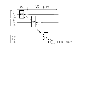
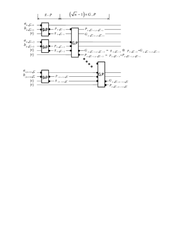
Fig. 5. Circuit flow for the first phase.
Note FA and HA are the full adder and the half adder, respectively. and are initially , and and are summation and carry for each position, respectively.
Fig. 5. Circuit flow for the first phase.
Note FA and HA are the full adder and the half adder, respectively. and are initially , and and are summation and carry for each position, respectively.
![[Uncaptioned image]](/html/1008.5093/assets/x7.png)
Fig. 6. Circuit flow for the second phase.
Col-carry block generates a column-level carry output, which is used for the actual incoming carry value for the next (right) column.
Fig. 6. Circuit flow for the second phase.
Col-carry block generates a column-level carry output, which is used for the actual incoming carry value for the next (right) column.
![[Uncaptioned image]](/html/1008.5093/assets/x8.png)
Fig. 7. Circuit flow for the third phase.
c represents the block for generating carry output for -th position. SUM is for generating the final summation value for -th position.
Fig. 7. Circuit flow for the third phase.
c represents the block for generating carry output for -th position. SUM is for generating the final summation value for -th position.
2.4 Clearing Ancillae Qubits
As shown in Table 3.2, three types of ancillae qubits are used, , , and . To clean these ancillae, we have used the strategy proposed in Reference [14]. The key idea of this approach is based on the observation that in two’s complement arithmetic
| (14) | |||||
| (15) | |||||
| (16) |
where is the bit-wise inversion of . Let us consider an addition of and , , where and are the bitwise sum and carry vectors, respectively. Let us consider another addition of and , , where and are sum and carry vectors, respectively. Note the bitwise sum is because
| (17) |
It is worth noting that must be equal to because of
| (18) | |||||
| (19) | |||||
| (20) | |||||
| (21) | |||||
| (22) | |||||
| (23) |
Now we follow the circuit as shown in Figure 2.4. Conceptually any addition circuit can be divided into two parts, generation ()and generation (). As shown in the figure, we apply as follows.
| (24) |
As the second step, we apply as follows.
| (25) |
Apply two operations
| (26) |
| (27) |
Meanwhile,
| (28) |
Since the two carry vectors and for and are the same, the above line changes to
| (29) |
Therefore, running the inverse operation,
| (30) |
Finally, apply as follows.
| (31) |
to generate the final sum and clean ancillae.
![[Uncaptioned image]](/html/1008.5093/assets/x9.png)
Fig. 8. Clearing Ancillae Qubits.
By applying the inverse of the carry generation flow, the ancillae qubits can be cleaned.
Fig. 8. Clearing Ancillae Qubits.
By applying the inverse of the carry generation flow, the ancillae qubits can be cleaned.
3 Analysis
3.1 Depth Analysis
To analyze the depth of the proposed adder, we have to decompose the circuit blocks into elementary gates, which can be decomposed into unit delay gates. In this work, we assume one-qubit, CNOT, and Control- gates have unit delay. The elementary gates we have chosen for constructing our circuits are SWAP, CCNOT, CNOT, Control-, and one-qubit gates. In this paper, we use the three-CNOT construction for SWAP gate. Figure 3.1 shows the conventional form of CCNOT (left) and its decomposition into one-qubit and two-qubit gates (right).
![[Uncaptioned image]](/html/1008.5093/assets/x10.png)
Fig. 9. Circuit for CCNOT
Fig. 9. Circuit for CCNOT
3.1.1 Circuit Decomposition with NTC Constraints
Now we decompose the circuit blocks for three phases with the chosen elementary gates and necessary SWAP operations to satisfy the NTC constraints. The blocks are shown in Figures 3.1.1 to 3.1.1. The circuit of HALF ADDER is shown in Figure 10(a). Figure 10(b) [11] shows a decomposition of FULL ADDER into elementary gates. In this figure, there is no limitation on the distance between operands for a gate. To satisfy the NTC constraint, we redesign it as shown in Figure 10(c) by adding several SWAP gates to move the qubits to neighboring positions. This approach is also applied for the following circuit blocks. The circuits for g and p, and the generalized G and P are shown in Figure 3.1.1. The circuit of Column_carry is shown in Figure 3.1.1. For generating , a single CCNOT is enough. However, to propagate it to the next column and to propagate to the rows, a SWAP is necessary. For implementing the last SWAP gate in the neighbor interaction only case, several SWAPs are necessary as shown in Figure 12(b). The initial circuit for Carry is shown in Figure 13(a). Since the has to be moved to the upper row, several SWAPs are necessary as shown in Figure 13(b). After this circuit, the is transported to the top position, and the others are to the lower row. Since the carry for the first row is different from other rows, Figures 13(c) and 13(d) show its circuits. The circuits for SUM are shown in Figures 14(a) and 14(b). For the second and the first row, we have to use slightly different circuits as shown in Figures 14(c) and 14(d), and Figure 14(e), respectively.
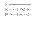
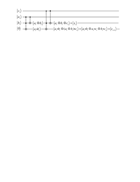

Fig. 10. Circuit for HALF ADDER (a); Circuits for FULL ADDER with arbitrary interaction (b) and with only nearest-neighbor interaction (c)
Fig. 10. Circuit for HALF ADDER (a); Circuits for FULL ADDER with arbitrary interaction (b) and with only nearest-neighbor interaction (c)
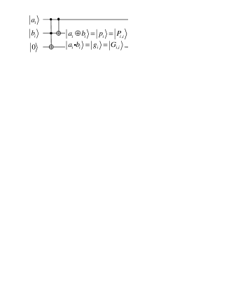
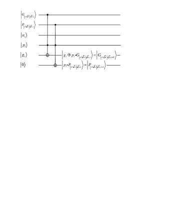

Fig. 11. Circuits for g,p (a); Circuits for G and P with arbitrary interaction (b) and with only nearest-neighbor interaction (c)
Fig. 11. Circuits for g,p (a); Circuits for G and P with arbitrary interaction (b) and with only nearest-neighbor interaction (c)
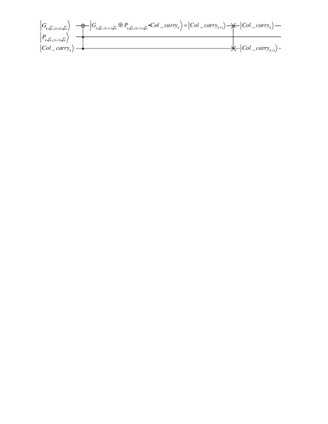

Fig. 12. Circuits for Column_carry with arbitrary interaction (a) and with only nearest-neighbor interaction (b)
Fig. 12. Circuits for Column_carry with arbitrary interaction (a) and with only nearest-neighbor interaction (b)
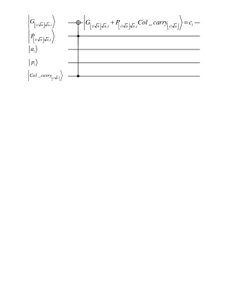

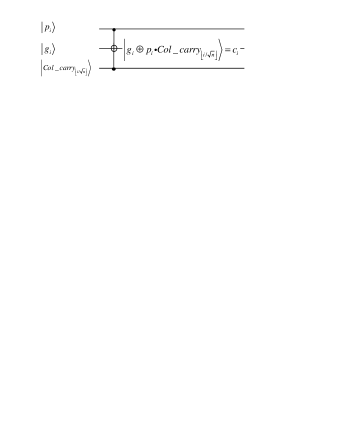

Fig. 13. Circuits for Carry with arbitrary interaction (a) and with only nearest-neighbor interaction (b); Circuits for Carry1 with arbitrary interaction (c) and with only nearest-neighbor interaction (d)
Fig. 13. Circuits for Carry with arbitrary interaction (a) and with only nearest-neighbor interaction (b); Circuits for Carry1 with arbitrary interaction (c) and with only nearest-neighbor interaction (d)
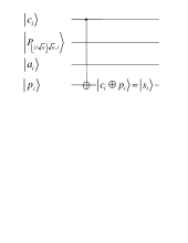

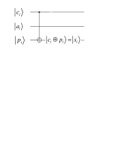


Fig. 14. Circuits for SUM with arbitrary interaction (a) and with only nearest-neighbor interaction (b); Circuits for SUM1 with arbitrary interaction (c) and with only nearest-neighbor interaction (d); Circuit for SUM2 (e)
Fig. 14. Circuits for SUM with arbitrary interaction (a) and with only nearest-neighbor interaction (b); Circuits for SUM1 with arbitrary interaction (c) and with only nearest-neighbor interaction (d); Circuit for SUM2 (e)
3.1.2 Total Depth
Based on the revised circuits with satisfying the NTC constraint, we can summarize the depth of each elementary gate and circuit block as shown in Table 3.1.2.
Table 1. Depth analysis of each gate and circuit
Table 1. Depth analysis of each gate and circuit
Name Composition of the longest path # of unit-gate steps SWAP 3 CNOTs 3 CCNOT 1 SWAP + 6 unit gates 9 HALF ADDER 1 CCNOT + 1 CNOT 10 FULL ADDER 2 CCNOTs + 2 CNOTs + 2 SWAPs 26 g and p 1 CCNOT + 1 CNOT 10 G and P 2 CCNOTs + 6 SWAPs 36 Column_carry 1 CCNOT + 3 SWAPs 18 Carry 1 CCNOT + 4 SWAPs 21 Carry1 1 CCNOT + 2 SWAPs 15 SUM 1 CNOT + 4 SWAPs 13 SUM1 1 CNOT + 2 SWAPs 7 SUM2 1 CNOT 1
The proposed adder works in three sequential phases, and hence the overall depth is the sum of the depths for each phase. The depth for each phase is the “long pole”, or the longest delay among the parallel execution paths. In the first column, one HA and FA operations are executed sequentially. Since HA needs 10 unit-gate steps and FA needs 26 unit-gate steps, unit-gate steps are needed. On the other hand, the other columns need one g, p + (-1)G, P, which is . The overall depth for the first phase is the longer of the two column types, hence . The second phase consists of Column_carry operations, requiring a total of time steps. The third phase consists of Carry + Carry1 and SUM1 operations for the longest path. Hence, the depth is unit-gate steps. By summing depths of each phase, the total depth is .
The above depth is only for generating the summation output without clearing the ancillae. For clearing ancillae, we apply more circuits as shown in Figure 2.4. Based on this figure, we can decompose the above three phases into the carry generation flow and the sum generation flow. The first and the second phases are for the carry generation flow. The third phase has to be divided into the carry generation flow and the sum generation flow. The above depth is apportioned as for carry generation flow and for sum generation flow. As shown in Figure 2.4 we need to apply NOT and CNOT gates and then inverse of the carry generation flow again with the final NOT gate. Hence, the overall depth is .
3.2 Required Space
The number of qubits for the adder is shown in Table 3.2. As shown in the first column, some qubits work for multiple purposes. Note the additional number of qubits is , which is less than twice the minimum qubits [12, 15].
Table 2. Number of Qubits
Table 2. Number of Qubits
Name Number of qubits Explanation Input Input , Carry propagate for -th position, and Summation Carry generation for -th position, Carry generation between and , and carry for -th position Carry propagation between and Inter column carry. The last is for the final carry output. Total ()+() Mandatory + Additional
3.3 Comparison to Other Adders
Table 3. Comparison with Other Designs
Table 3. Comparison with Other Designs
When only interactions between neighboring qubits are allowed, the depth of arithmetic circuits increases. For the 2D case, the depth lower bound was proven to be [22]. Therefore, the depth of the proposed adder is asymptotically optimal.
Beyond the asymptotic behavior, it seems more interesting and important to compare with other adders in the practical cases. Specifically, it is necessary to compare adders designed for the 1D NTC architecture since they can be implemented on the 2D NTC architecture without modification, using a simple serpentine qubit layout. The overall analysis and the comparison between the adders are shown in Table 3.3. The first column distinguishes the architecture and the second column lists the adder type. For the 1D NTC architecture, we choose three typical adders. Vedral et al. proposed a plain ripple-carry adder [6], named VBE in the table. VBE-Improved is the Van Meter and Itoh update to this adder [18]. Cuccaro et al. proposed a ripple carry adder with only one ancillae qubit [12], named CDKM. For the 2D NTC architecture, the present adder is shown. For the architecture with arbitrary distance interaction, several adders are evaluated. Draper proposed a quantum Fourier transform adder [13], named QFT-based. By exploiting the classical fast addition algorithm, Draper et al. also proposed a carry-lookahead adder [14], named CLA-based. Kawata et al. also proposed an adder based on the combination of ripple carry adder and carry-lookahead adder [24], named RCA+CLA-based. For comparison, the depth and the size of each adder is shown in the third column. In this work, the depth is measured by in units of one- and two-qubit gates for the 1D and 2D NTC architectures. On the other hand, the depth for the AC architecture is based on one-, two-, and CCNOT gates. The size is for the number of qubits for input, output, and ancillae. In the fourth column, the input size is shown when the selected adder works faster than the present adder. In the fifth column, we calculate KQ, the product of qubits and depth where and are the numbers of logical qubits and computational steps, respectively [23]. KQ is used to estimate the strength of error correction required.
From this table we can point out three key results. First, when the size of input is larger than 58, the present adder works faster than 1D NTC adders. Second, the present adder needs about two times number of qubits than 1D NTC adders. Lastly, the present adder has a smaller KQ factor when the input size is larger than 278.
4 Conclusion and Open Problems
In this work, we proposed a quantum adder for the 2D NTC architecture for the first time. Van Meter and Oskin indicated that an adder would be in time complexity on a 2D architecture, but no circuit has been provided [25]. The proposed adder has the depth complexity with qubits. We found that the proposed adder works faster than a 1D ripple-carry adder when the length of the input registers is larger than 58, and requires about two times the number of additional qubits.
Although this adder is, to the best of our knowledge, the first one specifically designed for a 2D architecture, we suspect it will not be the last; we anticipate that several improvements are possible. First, the number of additional gates is very large. Most of the gates for the proposed adder are used for transporting qubits to neighboring positions so that gates can be executed. By arranging qubits in a better way, we may be able to reduce the necessary propagattion operations. Second, the phase for cleaning the ancillae qubits roughly doubles the total number of quantum operations. In the present adder, the ancillae qubits are reinitialized by applying the inverse circuit, doubling the overall depth. Perhaps there is some way to reduce this drawback by exploiting some overlap of the clearing phase with the computation phase. Third, the number of ancillae is also very large. The proposed design attempts to achieve the highest parallel execution at the expense of requiring more ancillae, but this tradeoff may prove to be less than optimal for two reasons. First, qubits themselves are expensive resources, and in many applications could be allocated to other work if not used directly in the adder; second, inserting the ancillae into our layout increases the distance between qubits, forcing the addition of more SWAPs and slowing down the circuit.
Acknowledgements
This research is supported in part by the Japan Society for the Promotion of Science (JSPS) through its Funding Program for World-Leading Innovative R&D on Science and Technology (FIRST Program), and in part by the National Research Foundation of Korea Grant funded by the Korean Government(Ministry of Education, Science and Technology).[NRF-2010-359-D00012]
References
References
- [1] Peter W. Shor. Polynomial-time algorithms for prime factorization and discrete logarithms on a quantum computer. SIAM Journal on Computing, 26(5):1484–1509, 1997.
- [2] Lov K. Grover. A fast quantum mechanical algorithm for database search. In STOC ’96: Proceedings of the twenty-eighth annual ACM symposium on Theory of computing, pages 212–219, New York, NY, USA, 1996. ACM.
- [3] Michele Mosca. Quantum algorithms. http://arxiv.org/abs/0808.0369, 2008.
- [4] Dave Bacon and Wim van Dam. Recent progress in quantum algorithms. Communications of the ACM, 53(2):84–93, 2010.
- [5] Katherine L. Brown, William J. Munro, and Vivien M. Kendon. Using quantum computers for quantum simulation. http://arxiv.org/abs/1004.5528, 2010.
- [6] Vlatko Vedral, Adriano Barenco, and Artur Ekert. Quantum networks for elementary arithmetic operations. Phys. Rev. A, 54(1):147–153, Jul 1996.
- [7] David Beckman, Amalavoyal N. Chari, Srikrishna Devabhaktuni, and John Preskill. Efficient networks for quantum factoring. Phys. Rev. A, 54(2):1034–1063, Aug 1996.
- [8] Edward Fredkin and Tommaso Toffoli. Conservative logic. International Journal of Theoretical Physics, 21:219–253, 1982.
- [9] Richard P. Feynman. Feynman Lectures on Computation. Addison Wesley, 1996.
- [10] Andrew S. Glassner. Quantum computing, part 2. IEEE Computer Graphics and Applications, 21(5):86–95, 2001.
- [11] Kai-Wen Cheng and Chien-Cheng Tseng. Quantum full adder and subtractor. Electronics Letters, 38(22):1343–1344, Oct 2002.
- [12] Steven A. Cuccaro, Thomas G. Draper, Samuel A. Kutin, and David Petrie Moulton. A new quantum ripple-carry addition circuit. http://arxiv.org/abs/quant-ph/0410184, 2004.
- [13] Thomas G. Draper. Addition on a quantum computer. http://arxiv.org/abs/quant-ph/0008033, 2000.
- [14] Thomas G. Draper, Samuel A. Kutin, Eric M. Rains, and Krysta M. Svore. A logarithmic-depth quantum carry-lookahead adder. http://arxiv.org/abs/quant-ph/0406142, 2004.
- [15] Yasuhiro Takahashi and Noboru Kunihiro. A linear-size quantum circuit for addition with no ancillary qubits. Quantum Information and Computation, 5(6):440–448, 2005.
- [16] Tzvetan S. Metodi and Frederic T. Chong. Quantum Computing for Computer Architects. Synthesis Lectures on Computer Architecture. Morgan & Claypool Publishers, 2006.
- [17] Dmitri Maslov, Sean M. Falconer, and Michele Mosca. Quantum circuit placement. IEEE Transactions on Computer-Aided Design of Integrated Circuits and Systems, 27(4):752–763, April 2008.
- [18] Rodney Van Meter and Kohei M. Itoh. Fast quantum modular exponentiation. Phys. Rev. A, 71(5):052320, May 2005.
- [19] D. Kielpinski, C. Monroe, and D. J. Wineland. Architecture for a large-scale ion-trap quantum computer. Nature, 417(6890):709–711, June 2002.
- [20] Adriano Barenco, Charles H. Bennett, Richard Cleve, David P. DiVincenzo, Norman Margolus, Peter Shor, Tycho Sleator, John A. Smolin, and Harald Weinfurter. Elementary gates for quantum computation. Phys. Rev. A, 52(5):3457–3467, Nov 1995.
- [21] Andrew M. Steane. Space, time, parallelism and noise requirements for reliable quantum computing. Fortschritte der Physik, 46(4-5):443–457, 1998.
- [22] Byung-Soo Choi and Rodney Van Meter. Effects of interaction distance on quantum addition circuits. http://arxiv.org/abs/0809.4317, 2008.
- [23] Andrew M. Steane. Overhead and noise threshold of fault-tolerant quantum error correction. Phys. Rev. A, 68(4):042322, Oct 2003.
- [24] Yoshinori Kawata, Satoshi Yayu, and Shuichi Ueno. An efficient quantum addition circuit : Extended abstract. IEICE Technical Report. Circuits and systems, 107(527):95–96, March 2008.
- [25] Rodney Van Meter and Mark Oskin. Architectural implications of quantum computing technologies. ACM Journal on Emerging Technologies in Computing Systems, 2(1):31–63, 2006.