Highly Confined Hybrid Spoof Surface Plasmons in Ultra-thin Metal/Dielectric Heterostructures
Abstract
Highly confined “spoof” surface plasmon-like (SSP) modes are theoretically predicted to exist in a perforated metal film coated with a thin dielectric layer. Strong modes confinement results from the additional waveguiding by the layer. Spectral characteristics, field distribution, and lifetime of these SSPs are tunable by the holes’ size and shape. SSPs exist both above and below the light line, offering two classes of applications: “perfect” far-field absorption and to efficient emission into guided modes. It is experimentally shown that these plasmon-like modes can turn thin, weakly-absorbing semiconductor films into perfect absorbers.
pacs:
73.20.Mf, 42.79.Dj, 42.25.Bs, 78.20.CiIntroduction. The surface plasmon (SP) is one of the linchpins of the field of sub-diffraction optics barnes_nature03 : by penetrating below the metal surface Raether_book , electromagnetic waves can be localized beyond diffraction limit. This opens a wide range of applications in spectroscopy, photonic circuits, solar cells, and other technologically important areas halas_natphot07 ; Atwater ; bozh_nature06 . For longer wavelengths, metals begin resembling perfect electric conductors (PECs), wave penetration into the metal becomes negligible, and other approaches to light localization and concentration must be found. It has been recently discovered Pendry_sc ; Abajo_PRL ; Abajo_OptExp ; Abajo_Review ; Maier that SPs can be mimicked by perforating the metal surface with an array of sub-wavelength holes. Dispersion and confinement of the resulting “spoof” surface plasmons (SSPs) are defined (and can be tuned) by the holes’ size and geometry. Thus, the SSP-based approach to light confinement is crucial for bringing the advantages of plasmonics into the longer-wavelength spectral range, which is especially important for various infrared applications, including surface-enhanced infrared absorption (SEIRA) spectroscopy Ozawa_JPC91 ; Halas_CPL08 , on-chip light sources brongersma_optexp08 , and infrared detectors painter_optexp10 ; shawnlin_NL10 .
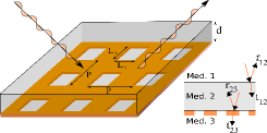
A major drawback of SSPs supported by metal films with simple perforation geometries (e.g., circular or rectangular holes) is that they are very weakly confined for most frequencies and, therefore, are not suitable for the above applications. More sophisticated geometries that have been shown Maier ; Sambles_PRL to improve confinement in the microwave spectral range are not practical for optical applications. In this Letter, we resolve the problem of poor confinement of conventional SSPs while retaining their important advantage: the ability to control SSP’s frequency and refractive index using variable size and shape of the metal holes. This is achieved by combining metal structuring with the traditional method of electromagnetic field confinement, waveguiding. We theoretically predict and experimentally confirm that a new class of SSPs exists in the ultrathin heterostructure comprised of a slab of high-index dielectric material and a perforated metal film (Fig. 1). The resulting SSPs owe their unusual electromagnetic properties to their hybrid nature: the conventional SSP modes inherent to any periodic metal structure are hybridized with conventional modes of dielectric films: guided waves (GW) and leaky Fabry-Perót (FP) modes. The hybrid SSPs represent an important improvement on both conventional guided modes and SSPs: they are better confined than either one of the two (Fig. 3), while their spectral properties and lifetimes are controllable by the size and shape of the metallic perforations. As a specific example and possible application of the proposed concept, we demonstrate that hybrid SSPs can turn low-absorbing semiconductor (specifically, SiC) films into near-perfect absorbers of infrared radiation. The choice of SiC owes to the strong dependence of its dielectric permittivity on frequency : changes by a factor as changes by neuner_jpc10 .
Theoretical description. It is instructive to start the theoretical description of hybrid SSPs by considering the eigenmodes (both leaky and fully-confined) of the unperforated heterostructure. Mathematically, this is done by recalling the standard Airy expression born_and_wolf for the reflectivity coefficient of the heterostructure :
| (1) |
where the reflection (transmission) coefficients () at the -th/-th medium interface are illustrated by Fig. 1, accounts for multiple reflections, and is the propagation wave number normal to the interface. All eigenmodes of the unperforated heterostructure (including leaky and fully-guided modes) correspond to the poles of . These poles are given by =, giving rise to the following necessary condition that must be satisfied by any eigenmode:
| (2) |
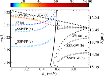
where is an integer number. Thin dielectric films with correspond to =, which will be assumed here. Note that = in the case of unperforated PEC film, and the phase of the Fresnel’s reflection coefficient satisfies = above the light line, but can depart from zero below the light line. The frequencies of the two eigenmodes found by solving for real wavenumbers along the interface correspond to the two eigenmodes: (i) the leaky FP mode above the light line, and (ii) the confined GW mode below the light line. For a specific case of a SiC film with thickness nm, the dispersion relations for these two eigenmodes are plotted in Fig. 2. For , the FP mode satisfies the quarter-wavelength condition =. Because the FP mode is leaky, it has a low quality factor . However, coupling to the GW mode requires a high-index prism or a diffraction grating, and its is limited only by the material losses. As shown below, when the metal film is patterned, both FP and GW modes can hybridize with SSPs giving rise to highly confined modes whose spectral properties can be tuned by the size and shape of the perforations, and whose confinement drastically exceeds that of either the SSPs or the modes of the unperforated structure (GW and FP modes).
Next, we consider a periodically perforated metal film as shown in Fig. 1. SSPs are introduced by generalizing Eq. (1) to include the effects of diffraction on the periodic hole array. Specifically, using the standard scattering matrix formulation, the reflection coefficient, which connects different diffractive orders, is expressed in the matrix form:
| (3) |
where is the multi-pass matrix given by . Because of the sub-wavelength periodicity of the hole array, the diagonal matrix element = expresses the experimentally-accessible reflection coefficient. Complex eigenfrequencies of the hybrid SSPs correspond to the roots of the equation =.
To make a further connection of hybrid SSPs to the modes of unperforated heterostructure, we introduce two effective (tilded) complex quantities for a perforated film: and . By comparing Eq. (1) to Eq. (3) and by using the above definitions, we find that
| (4) |
where involves summation over all the reciprocal lattice vectors (i.e., all the diffracted orders). These intuitive definitions of the effective quantities enable us to use the scalar Eqs. (1, 2) by replacing transmission/reflection coefficients and the corresponding phases with their effective counterparts. For example, the modified resonant phase-matching condition expressed by Eq. (2) is obtained by replacing = with , which can considerably deviate from . As will be shown below, the size and shape of the hole can strongly influence , thereby shifting the absorption peak from the Fabry-Perót resonance =.
Assuming a square array of holes in the PEC metal with the sub-diffraction period m and a thin SiC film with nm, we calculated the scattering matrices ( and ) using the semi-analytic modal matching technique Martin-Moreno_PRL , and analytically continued it into the complex -plane. The resulting dispersion curves for hybrid SSPs both above (leaky SSPs) and below (confined SSPs) the light line are plotted in Fig. 2, where =(a,b,c) labels the hole size (see caption), and the color indicates the quality factor of the modes.
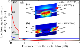
First we focus on dispersion curves below the light line: the guided mode of the unperforated structure GW(a), and the two hybrid SSPs (SSP/GW(b) and SSP/GW(c)) whose dispersion curves are controlled by the square holes’ size. As the hole size increases, the dispersion curves depart from the light line, thereby indicating high spatial confinement. Flattening of the dispersion curves for larger hole sizes also indicates an increasing density of states which can be utilized for plasmon-enhanced infrared emission brongersma_optexp08 . Strong concentration of the magnetic field of the hybrid SSP/GW mode inside the hole (Fig. 3 inset (a)) explains the high sensitivity of this mode to the size and shape of the hole. Figure 3 illustrates that the confinement of the SSP/GWs exceeds that of both classes of waves (GWs and pure SSPs without the dielectric film) from which these hybrid SSPs originate. The figure shows energy profiles of three modes at the particular subwavelength frequency, corresponding to a SSP/GW(c) mode at (i), a GW mode of the unperforated structure (ii), and a pure SSP of a thick perforated metal film surrounded by air (iii). Clearly, the hybrid SSPs have the highest confinement and the highest concentration of energy inside the dielectric film: () of the SSP/GW (GW) mode resides outside of the dielectric slab.
Hybridization between FP modes and SSPs produce leaky hybrid SSPs above the light line as shown in Fig. 2 by the progression from FP to SSP/FP modes. These hybrid leaky SSPs have a similar three-dimensional magnetic field profile to that of the guided SSP/GW modes as shown in the inset (a) to Fig. 3. Because fields are concentrated inside the perforation, spectral properties and the lifetime of the SSP/FP modes are strongly affected by the holes’ size . Their transverse confinement also significantly exceeds that of FP modes as indicated by Q-factor shown by color in Fig. 2. The SSP/FP mode lifetime and field confinment both increase with . The corresponding energy density profiles are similar to those plotted for the confined modes in Fig. 3. Note that, in addition to the SSP/FP modes, there is another leaky hybrid SSP labeled SSP/GW(j) above the light line whose field distribution (shown in Fig. 3 inset (b)) is centered outside of the hole. Therefore, the spectral position of the leaky SSP/GW modes is not strongly affected by the holes’ dimensions. Because SSP/FP and SSP/GW modes are leaky above the light line, they can be experimentally observed using conventional infrared spectroscopy as presented below.
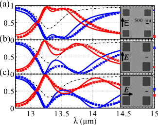
Experimental results. A SiC film of thickness = nm was hetero-epitaxially grown on a Si(100) substrate wafer, and an air-bridged membrane with area (m)2 was produced after KOH back-etching of the Si substrate. A nm Au film was thermally deposited on the newly exposed side of the SiC. Metal perforations were produced using a focused ion beam over a (m)2 area. Optical characterization (reflection, transmission) was performed using a Thermo Scientific Continuum microscope coupled to a Nicolet 6700 FTIR Spectrometer. Incident radiation was linearly polarized using a wire grid polarizer. In all measurements, transmission was less than . Therefore, we will focus on reflectivity and absorptivity spectra for the rest of this Letter. First, we measured prior to perforating the metal film which is shown by dot-dashed lines in Fig. 4. The broad reflection dip at =m corresponds to coupling to FP mode.
Next, we measured and for the perforated metal structures and plotted them alongside the results of the finite-elements COMSOL simulations in Fig. 4. Two hole sizes were used as perforations: small square holes (Fig. 4(a)) and larger rectangular holes (Fig. 4(b,c)). As predicted by the theory of hybrid SSPs, reflectivity curves reveal two reflection minima, which also correspond to absorption maxima. Thus, the metal perforation causes to drop to zero and absorption to reach nearly unity. The physical reason for this enhanced absorptivity is resonant coupling to leaky SSP/FP (long-wavelength peak) and SSP/GW (short-wavelength peak) modes.
Experimental results confirm that the spectral position of the SSP/GW dip (=m) is almost independent of the size/shape of the holes, while that of SSP/FP dip is very sensitive to hole size and, for rectangular holes, is polarization-sensitive. The SSP/FP absorption peak (e.g., at =m for light polarized along the short dimension of the large rectangular hole) is especially remarkable because it occurs far from the FP resonance in the spectral region where SiC is not very absorptive: =+. Without perforation, the round-trip absorptivity of the = SiC film is only =. This absorption enhancement is caused by the excitation of the high- SSP/FP mode which strongly traps and enhances the electromagnetic field inside the weakly-absorbing film, turning it into a “perfect” absorber.
Another degree of freedom to confine electromagnetic energy is to use more sophisticated hole shapes that exhibit site (or shape) resonances Sambles_PRL ; Maier . For example, a strong confinment even in a thinner heterostructures can be accomplished by employing relatively simple (and feasible for fabrication) U-shaped holes Rockstuhl shown in Fig. 5(a). For instance, in the case of the SSP/FP resonance, use of U-shaped holes causes even more dramatic red-shifting which facilitates trapping of electromagnetic fields by a subwavelength thick heterostructure. A family of reflectivity spectra shown in Fig. 5(b) correspond to U-shapes with increasing metal “tongue” length (see inset to Fig. 5(a)). The figure indicates that, counter-intuitively, the spectral position of the reflection dip red-shifts even as the remaining hole area decreases with increasing . This effect is due to the LC-like resonances of the U-shape occurring for electric field polarized parallel to the tongue Rockstuhl . This resonance manifests itself in the increased effective reflection phase . obtained for both rectangular and U-shaped holes at the respective reflectivity dips is shown by crosses and circles in Fig. 5(a) as a function of and , respectively. The U-shape’s parameter has a more pronounced effect on (and, by extension, on the spectral position of the reflection dip) than the overall size of the rectangular hole. In the latter case, the reflection phase saturates around the value of 1.25, while in the case of the U-shaped holes, approaches , with high value of indicating strong sensitivity to the geometry of the U-shape.
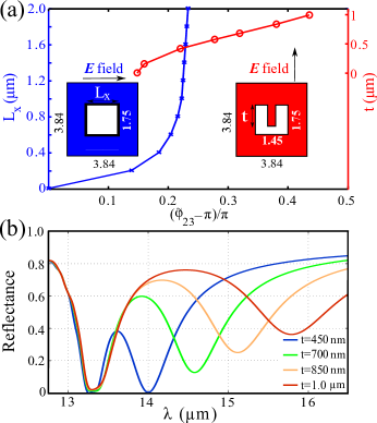
In conclusion, we have predicted and experimentally demonstrated that a heterostructure comprised of a periodically perforated metal film coated with high-index dielectric layer supports strongly confined hybrid spoof surface plasmons. This extraordinary confinement is achieved through hybridization between two weakly confined sets of modes: SSPs supported by the perforated metal film and guided modes supported by the dielectric layer. Hybrid SSPs retain tunability due to strong sensitivity to the holes’ size and shape. As an experimental proof of principle, we have demonstrated that hybrid SSPs can turn weakly-absorbing ultra-thin semiconductor films into spectrally-tunable “perfect” absorbers. Hybrid SSPs may find practical applications in multi-spectral infrared imaging, thermophotovoltaics, on-chip light sources, and infrared detectors.
This work was supported by NSF Grants ECCS-0709323 and CMMI-0928664, and the AFOSR MURI Grants FA9550-06-1-0279 and FA9550-08-1-0394.
References
- (1) W. L. Barnes, A. Dereux, and T. W. Ebbesen, Nature 424, 824 (2003).
- (2) H. Raether, Surface Plasmons on Smooth and Rough Surfaces and on Gratings, (Springer, Berlin, 1988).
- (3) S. Lal, S. Link, and N. J. Halas, Nature Phot. 1, 641 (2007).
- (4) H. A. Atwater and A. Polman, Nature Mat. 9, 205 (2010).
- (5) S. I. Bozhevolnyi, V. S. Volkov, E. Devaux, J.-Y. Laluet, and T. W. Ebbesen, Nature 440, 508 (2006).
- (6) J. B. Pendry, L. Martín-Moreno, and F. J. García-Vidal, Science 305, 847 (2004).
- (7) F. J. García de Abajo and J. J. Sáenz, Phys. Rev. Lett. 95, 233901 (2005).
- (8) X. M. Bendana and F. J. García de Abajo, Opt. Exp. 17, 18826 (2009).
- (9) F. J. García de Abajo, Rev. Mod. Phys. 79, 1267 (2007).
- (10) M. J. Lockyear, A. P. Hibbins, and J. R. Sambles, Phys. Rev. Lett. 102, 073901 (2009).
- (11) M. Navarro-Cía, M. Beruete, S. Agrafiotis, F. Falcone, M. Sorolla, and S. A. Maier, Opt. Exp. 17, 18184 (2009).
- (12) M. Osawa and M. Ikeda, J. Phys. Chem. 95, 9914 (1991).
- (13) J. Kundu, F. Le, P. Norlander, and N. J. Halas, Chem. Phys. Lett. 119, 452 (2008).
- (14) J. Rosenberg, R. V. Shenoi, S. Krishna, and O. Painter, Opt. Exp. 18, 3672 (2010).
- (15) A. C. Hryciw, Y. C. Jun, and M. L. Brongersma, Opt. Exp. 17, 185 (2008).
- (16) C-C. Chang, Y. D. Sharma, Y-S. Kim, J. A. Bur, R. V. Shenoi, S. Krishna, D. Huang, and S-Y. Lin, Nano Letters 10, 1704 (2010).
- (17) B. Neuner III, D. Korobkin, C. Fietz, D. Carole, G. Ferro, and G. Shvets, J. Phys. Chem. C 114, 7489 (2010).
- (18) M. Born and E. Wolf, Principles of Optics (Pergamon Press, New York, 1980), 6th ed.
- (19) L. Martín-Moreno, F. J. García-Vidal, H. J. Lezec, K. M. Pellerin, T. Thio, J. B. Pendry, and T. W. Ebbesen, Phys. Rev. Lett. 86, 1114 (2001).
- (20) C. Rockstuhl, T. Zentgraf, T. P. Meyrath, H. Giessen, and F. Lederer, Opt. Exp. 16, 2080 (2008).