Enhancement of the zero phonon line emission from a single NV-center in a nanodiamond via coupling to a photonic crystal cavity
Abstract
Using a nanomanipulation technique a nanodiamond with a single nitrogen vacancy center is placed directly on the surface of a gallium phosphide photonic crystal cavity. A Purcell-enhancement of the fluorescence emission at the zero phonon line (ZPL) by a factor of is observed. The ZPL coupling is a first crucial step towards future diamond-based integrated quantum optical devices.
Quantum information processing (QIP) has become one of the major research topics in quantum optics.1 As QIP requires the control of complex quantum systems several research groups have been striving for ways to realize an integrated quantum technology platform.2 Apart from purely semiconductor based approaches3 diamond has emerged as an interesting alternative. Several optically active defect centers in diamond have been studied on the single center level. The most promising among them for QIP applications is the nitrogen vacancy (NV)-center.4; 5 With its triplet ground state it is capable to encode quantum bits which can be controlled and read out by microwave or optical fields. In ultra-pure diamond, electron spin coherence times are in the millisecond range.6 Apart from this, the NV-center is probably the best known solid state single photon source operating at room temperature.7
However, the optical properties of the NV-centers are not ideal: The coupling strength to the electromagnetic field is small compared to other systems like quantum dots.8 Another problem is the small Debye-Waller factor. Even at cryogenic temperatures only a small fraction of about 3% of the radiation is emitted into the Fourier-limited zero phonon line (ZPL). 9
It has been proposed to overcome these problems by coupling the NV-centers to optical microcavities,10; 9 where the spontaneous emission (SE) rate is enhanced by the Purcell effect. For a perfect spatial and spectral matching of the emitter’s dipole with the cavity, the SE rate enhancement into the cavity mode is described by the Purcell factor
| (1) |
where is the wavelength at the cavity resonance in the medium, is the cavity quality factor (-factor) and is the effective mode volume. Increasing the SE rate into the ZPL will allow the generation of a large number of indistinguishable single photons 10 needed for linear optics quantum computation.11
An even stronger enhancement of the emitter-cavity coupling may bring the system to the strong coupling regime of cavity quantum electrodynamics, which allows the realization of quantum gates and interfaces between stationary and flying Qbits. Several attempts have been pursued to couple NV-centers to cavities such as microsphere resonators12; 13, microtoroids,14; 15 or photonic crystal cavities (PCC).16; 17 PCCs have the particular advantage that they can be fabricated with high quality factors as well as small mode volumes 18, both being figures of merit for obtaining a large Purcell enhancement. Furthermore, PCCs can easily be integrated into more complex systems of coupled cavities and waveguides.19
In this letter we present an experimental realization of one of the most crucial steps for integrated diamond-based quantum technology, i.e. the coupling of the ZPL of an NV-center in a nanodiamond to a single mode of a PCC.
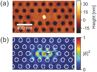
To achieve this, a free-standing photonic crystal slab (lattice constant 200 nm) with a so-called L3 cavity, formed by three missing holes (see Fig. 1), is designed using FDTD simulations (Lumerical). It is optimized to have the fundamental mode at 640 nm, slightly above the ZPL of the NV-center. The volume of the fundamental mode is . These structures were fabricated from a 70 nm thick heteroepitaxial gallium phosphide (GaP) layer,20 deposited on a Si(100) substrate by electron beam lithography and subsequent dry-etching.
Using a home-build micro photoluminescence setup (PL) with a numerical aperture (NA) of , bare cavities were analyzed utilizing the intrinsic fluorescence light under strong excitation with a green 532 nm laser (300 W). The intrinsic fluorescence is strongly enhanced at the cavity resonance. All the fabricated cavities show resonances around 642 nm with a typical deviation of nm and a -factor of around 1000.
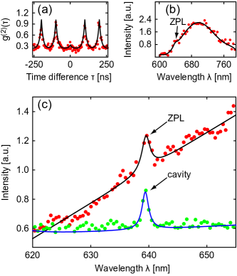
To place a single nanodiamond (height 35 nm) with a single NV-center in the cavity, first a diamond suspension was spin-coated onto a glass cover slip. These diamonds were then optically pre-characterized using a confocal microscope (NA ) with a Hanbury-Brown and Twiss setup under pulsed excitation with a 532 nm laser at a repetition rate of 10 MHz. For a diamond containing a single NV-center the autocorrelation function vanishes at ns. Figure 2(a) shows the measured function of a single nanodiamond. The interval between the peaks represents the repetition time of the pulsed laser. In contrast to what is expected from classical light there is no peak at ns, showing that the diamond contains only a single NV-center. Using our recently developed pick-and-place technique 21 this pre-selected diamond was picked up with an atomic force microscope (AFM) and preliminary placed on the GaP surface, close to the PCCs. Here the diamond was further characterized. In particular, a spectrum was measured [Fig. 2(b)] and the position of the ZPL at nm was determined [red dots in Fig. 2(c)].
We selected a cavity with a resonance wavelength of nm and a -factor of and performed active tuning to the ZPL of this diamond in the following way: A focused blue laser (407 nm, 270 W), which is absorbed within the GaP membrane, was used to heat the structure locally for several minutes. It is assumed that by this procedure the GaP locally oxidizes and changes its index of refraction.22 After this procedure the cavity’s resonance was blue shifted by nm and showed a resonance at nm. The quality factor decreased from to . Figure 2(c) shows the fluorescence spectra of the bare cavity after tuning and the fluorescence from the NV-center. Note that the cavity resonance wavelength matches the ZPL almost perfectly.
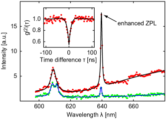
In a last step the diamond was picked up again using the AFM and placed now in the center of the cavity [Fig. 1(a)]. Since the field strength of the cavity mode decays exponentially outside the slab, it is crucial to place the NV-center as close as possible to the surface.17 In the AFM images the diamond shows a height of about 35 nm, meaning that the NV-center is less than 35 nm above the surface. Figure 3 shows the measured spectra of the cavity with and without the nanodiamond, both taken at 300 W excitation power. The pronounced enhancement of the ZPL emission at 639.5 nm is striking. The autocorrelation measurement (inset in Fig. 3) proves that the light emitted from the cavity has a strong non-classical behaviour, revealing that the fluorescence mainly originates from the NV-center. The peaks around 610 nm stem from higher-order modes with smaller -factors. As no influence of the NV-center on the fluorescence intensity is expected below 620 nm, the two spectra were normalized with respect to the emission at 600 nm to compensate for a slightly different alignment. This allows to reveal which part of the cavity’s fluorescence (red curve in Fig. 3) has it’s origin in the NV-center by subtracting the (normalized) bare cavity background (green curve in Fig. 3).
To quantify the observed enhancement in the ZPL, we calculate the spectrally resolved SE enhancement due to the cavity by comparing the ZPL emission in the cavity and on the bare substrate. We would like to point out that care has to be taken when comparing the optical properties of a bare defect center and one coupled to a photonic structure. Any change in the dielectric environment also influences the corresponding emission properties such as the overall SE rate 17. However, the spectral shape is changed only near the cavity resonances. This allows us to normalize the measured NV-spectra [Fig. 2(c) and Fig. 3] to the broad spectral region above and below the ZPL. Afterwards, a Lorentzian was fitted to the data, resulting in (normalized) peak intensities of and on the substrate and on the cavity, respectively. This yields the experimental Purcell enhancement . The difference to the theoretical value , calculated from Eq. (1), is caused by non-ideal alignment. Neither is the NV-center placed in the field maximum of the cavity mode, nor is the dipole moment’s orientation optimized.
A further enhancement of the emission into the ZPL can be achieved by improving the -factor or by performing experiments at cryogenic temperatures. At 4 Kelvin the ZPL can be nearly Fourier-limited 24 and about 3 of the light is emitted into the ZPL. In this case we estimate that coupling to a similar PCC with a -factor of 600 should allow channeling of almost of the emission into the cavity mode.
In conclusion, we have demonstrated the deterministic coupling of the zero phonon line of a single nitrogen-vacancy center in a nanodiamond to a photonic crystal cavity. This is a major step towards the realization of integrated quantum optical devices. With the presented pick-and-place technique and the selective cavity tuning, even more complex systems, involving two cavities and emitters, 23 can be assembled in a controlled way. Simple quantum gates, integrated on a single photonic crystal chip, are within reach.
This work was supported by the DFG (BE2224/9) and the BMBF (KEPHOSI). J. Wolters acknowledges funding by the state of Berlin (NaFöG).
References
- 1 T. D. Ladd, F. Jelezko, R. Laflamme, Y. Nakamura, C. Monroe, J. L. O’Brien, Nature 320, 1601 (2010).
- 2 J. L. O’Brien, A. Furusawa, J. Vuckovic, Nat. Photon. 3, 687 (2009).
- 3 K. Hennessy, I. Fushman, D. Englund, A. Faraon, N. Stoltz, P. Petroff, J. Vuckovic, Science, 320 5877 (2008).
- 4 F. Jelezko, J. Wrachtrup, Phys. Stat. Sol. (a) 203, 21 (2006).
- 5 D. DiVincenzo, Nat. Mat. 9, 468 (2010).
- 6 G. Balasubramanian, P. Neumann, D. Twitchen, M. Markham, R. Kolesov, N. Mizuochi1, J. Isoya, J. Achard, J. Beck, J. Tissler, V. Jacques, P. R. Hemmer, F. Jelezko, J. Wrachtrup, Nat. Mat. 8, 383 (2009).
- 7 R. Brouri, A. Beveratos, J.-P. Poizat, P. Grangier, Opt. Lett. 17, 1294 (2000).
- 8 K. Hennessy A. Badolato, M. Winger, D. Gerace1, M. Atatüre, S. Gulde1, S. Fält, E. L. Hu, A. Imamoglu, Nature 445, 896 (2007).
- 9 C Santori, P E Barclay, K.-M. C Fu, R. G. Beausoleil, S. Spillane, M. Fisch, Nanotechnology 21, 274008 (2010)
- 10 C.-H. Su, A. D. Greentree, L. C. L. Hollenberg, Opt. Expr. 16, 12 (2008).
- 11 E. Knill, R. Laflamme, G. J. Milburn, Nature 409, 46 (2001).
- 12 Y.-S. Park, A. K. Cook, and H. Wang, Nano Lett. 6, 2075 (2006).
- 13 S. Schietinger, T. Schröder, and O. Benson, Nano Lett. 8, 3911 (2008).
- 14 P. E. Barclay, C. Santori, K.-M. Fu, R. G. Beausoleil, and O. Painter, Opt. Express 17, 8081 (2009).
- 15 M. Gregor, R. Henze, T. Schröder, and O. Benson, Appl. Phys. Lett. 95, 153110 (2009).
- 16 M. Barth, N. Nüsse, B. Löchel, and O. Benson, Opt. Lett. 34, 1108 (2009).
- 17 D. Englund, B. Shields, K. Rivoire, F. Hatami, J. Vuckovic, H. Park, M. D. Lukin arXiv:1005.2204v1 (2010).
- 18 B.-S. Song, S. Noda, T. Asano, Y. Akahane, Nat. Mat. 1, 468 (2005).
- 19 M. Notomi, E. Kuramochi, T. Tanabe, Nat. Phot. 2, 741 (2008).
- 20 H. Döscher, T. Hannappel, B. Kunert, A. Beyer, K. Volz, W. Stolz, Appl. Phys. Lett. 93, 172110 (2008).
- 21 submitted (2010).
- 22 H. S. Lee, S. Kiravittaya, S. Kumar, J. D. Plumhof, L. Balet, L. H. Li, M. Francardi, A. Gerardino, A. Fiore, A. Rastelli, O. G. Schmidt, Appl. Phys. Lett. 95, 191109 (2009).
- 23 C.-H. Su, A. D. Greentree, , W. J. Munro, K. Nemoto, L. C. L. Hollenberg, Phys. Rev. A 78, 062336 (2008).
- 24 Y. Shen, T. M. Sweeney, H. Wang, Phys. Rev. B 77, 033201 (2008).


