Microstrip superconducting quantum interference device amplifiers with submicron Josephson junctions: enhanced gain at gigahertz frequencies
Abstract
We present measurements of an amplifier based on a dc superconducting quantum interference device (SQUID) with submicron Al-AlOx-Al Josephson junctions. The small junction size reduces their self-capacitance and allows for the use of relatively large resistive shunts while maintaining nonhysteretic operation. This leads to an enhancement of the SQUID transfer function compared to SQUIDs with micron-scale junctions. The device layout is modified from that of a conventional SQUID to allow for coupling signals into the amplifier with a substantial mutual inductance for a relatively short microstrip coil. Measurements at 310 mK exhibit gain of 32 dB at 1.55 GHz.
In recent years there have been many advances with amplifiers based on dc superconducting quantum interference devices (SQUIDs) with a resonant stripline input circuit Mück et al. (1998). In these devices the signal is coupled to the SQUID through the microstrip resonance formed by a superconducting spiral input coil above the dielectric layer on top of the superconducting washer that forms the SQUID loop. Such amplifiers have exhibited gains in excess of 20 dB in the radiofrequency range Mück and McDermott (2010) and noise temperatures at 500 MHz within a factor of two of the quantum limit Mück and Clarke (2001). In addition, microstrip SQUID amplifiers have been demonstrated at frequencies up to 7.4 GHz Mück et al. (2003). This suggests the possibility of using these devices for measuring the weak signals involved in various quantum information processing schemes with superconducting circuits Clarke and Wilhelm (2008), including dispersive readout with circuit quantum electrodynamics Wallraff et al. (2004) and schemes involving pulsed interactions between qubits and oscillators Serban et al. (2008). However, the shorter coils required to increase the operating frequency lead to decreased gain: 12 dB at 2.2 GHz and 6 dB at 7.4 GHz Mück et al. (2003). An alternative configuration with a small-area SQUID coupled in a lumped-element configuration to a quarter-wave resonator was shown to operate as an amplifier in the GHz range Spietz et al. (2008).

The gain of a microstrip SQUID amplifier is proportional to , where is the mutual inductance between the input coil and the SQUID loop and is the maximum voltage modulation of the SQUID. Pushing the operating frequency higher requires shorter coils, which necessarily reduces , although this reduction can be mitigated somewhat by modifying the SQUID loop and coil layout from the conventional washer design. Nonetheless, will decrease as is increased unless one can simultaneously compensate by increasing . The peak-to-peak voltage modulation of a SQUID is limited by the product of each junction, where and are the junction critical current and shunt resistance, respectively. Nonhysteretic device operation requires a junction damping parameter , where , thus placing an upper limit on , where is the junction self-capacitance. For Josephson junctions fabricated with conventional photolithography with an area of a few , is typically a few hundred fF. The other standard SQUID optimization, Tesche and Clarke (1977) constrains the product of the SQUID self-inductance and . Taking a typical set of dc SQUID parameters, pH, , fF, the maximum value of that maintains nonhysteretic operation is . This then results in a maximum flux-to-voltage transfer coefficient V/ Tesche and Clarke (1977). To enhance , one can reduce somewhat, but it then becomes difficult to avoid loss of gain due to the resulting reduction in .
Larger values of can be achieved by increasing , however, must be reduced in order to avoid hysteretic behavior. In this letter, we describe the fabrication of dc SQUIDs with submicron Josephson junctions patterned with electron-beam lithography and a device layout tailored to maintain large for short coil lengths. We present measurements of one of these SQUIDs operated as a microstrip SQUID amplifier, with gain in excess of 30 dB at GHz.
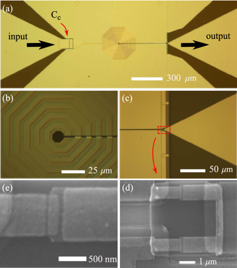
Our SQUID loop consists of a large Al washer on an oxidized Si wafer with a m-wide octagonal hole in the center and a m slit of length m extending to one side. Applying the standard washer-SQUID expressions Ketchen and Jaycox (1982) leads to an estimate for the SQUID inductance pH. The Al washer has an outer-width of 6.5 mm at its midpoint and also serves as the ground plane when the SQUID is operated as a microstrip SQUID amplifier, with cutouts allowing for the input and output traces to be coupled in a coplanar-waveguide geometry [Fig. 1(a)]. The dielectric layer on top of the washer is formed from a nm-thick SiO2 film deposited by PECVD. The Al input coil has a m linewidth and follows an octagonal path around the washer hole with a length of mm and a number of turns [Fig. 1(b)]. Our present design does not have a connection to the center turn of the coil, thus, a direct dc measurement of is not possible. Nonetheless, for our geometry we can estimate nH Ketchen et al. (1992). Between the input pad and the coil, we fabricated an on-chip input coupling capacitor that we estimate to be pF using the same dielectric layer as on the washer to reduce the loading from the environment on the microstrip resonance Kinion and Clarke (2008).
While the initial four layers of the SQUIDs are patterned photolithographically, the junctions are patterned in a final electron-beam lithography step and are formed with a double-angle shadow-evaporation process Dolan (1977). An in situ Ar ion mill step ensures superconducting contacts between the junction layer and the washer. The junctions are 730 nm 180 nm [Fig. 1(d-e)], from which we estimate the capacitance to be roughly 15 fF. The resistive shunts are formed from a 20 nm-thick Pd layer with a low-temperature sheet resistance of 6.1 resulting in .
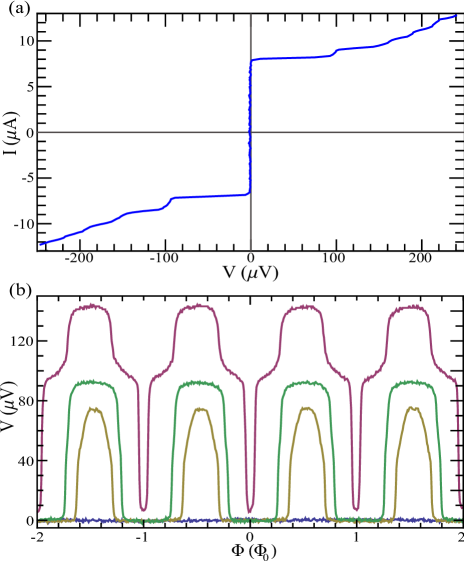
Prior to measuring the microwave response of the amplifier, we recorded the current-voltage characteristics (IVCs) at 310 mK on a separate cooldown of our 3He refrigerator [Fig. 2(a)]. From the IVCs, we observe A, corresponding to . Based on a one-parameter fit to the critical current modulation (not shown), we obtain , which, combined with is in reasonable agreement with our earlier estimate for . Measurements of the flux modulation of the dc voltage for different bias currents [Fig. 2(b)] allow us to extract , with a maximum value of mV/. We note that during subsequent measurements of gain on this device, was likely reduced somewhat due to noise fed back to the SQUID from the microwave post-amplifier.

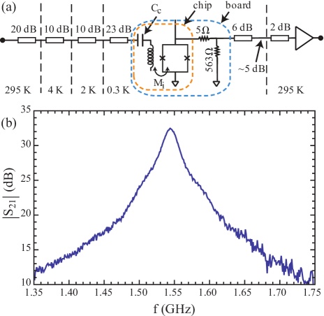
On a subsequent cooldown to 310 mK, we mounted the SQUID on a board with stripline traces attached with multiple short wirebonds to the input and output pads of the SQUID and multiple ground wirebonds to the washer. The bias current and flux bias for the SQUID were supplied with batteries and the lines passed through cryogenic Cu-powder filters. To shield the SQUID from external magnetic fields, the board was mounted in a closed Al box that was wrapped in Pb foil and a cryogenic metal shield surrounded the vacuum can of the refrigerator. The microwave path consisted of multiple stages of attenuation on the input side, including dB anchored to the 3He stage, for attenuating room-temperature noise, followed by a dB attenuator on the SQUID output for matching to [Fig. 3(a)]. For further amplification we used a room-temperature post-amplifier (3 x MiniCircuits ZX60-33) with a gain of 48 dB at 1.55 GHz. A dB attenuator at the input was necessary to help with matching the ZX60-33 to . We calibrated the various cable loss contributions, attenuation, and post-amplifier gain with a short coax piece in place of the SQUID board by measuring the transmission with a network analyzer during a separate cooldown of the refrigerator. Subsequent gain measurements of the SQUID were referred to this baseline.

We measured the gain of the SQUID amplifier using a network analyzer to supply a weak power to the input, dBm (Fig. 3). For the optimum bias current and flux values, we measured a maximum gain of 32 dB at 1.55 GHz with a bandwidth of 30 MHz. Upon tuning to the optimum point, the gain was stable and there was no evidence for self-oscillations that can sometimes be present for microstrip SQUID amplifiers under certain biasing and input conditions Kinion and Clarke (2010). A measurement of the noise temperature was not practical with the present configuration due to the substantial contribution from the room-temperature post-amplifier. Future measurements with a cryogenic HEMT amplifier should greatly reduce the noise contribution of the post-amplifier.
One potential concern with increasing the shunt size is the possibility for hot-electron effects leading to an elevated temperature for the shunts Wellstood et al. (1989, 1994). This can be addressed to some extent with metallic cooling fins added to the shunts Wellstood et al. (1989). In addition, the enhanced gain resulting from the larger shunts should at least partially compensate any excess noise due to hot-electron effects in the shunts.
In conclusion, we have fabricated microstrip SQUID amplifiers with Al-AlOx-Al submicron junctions. From low frequency measurements, we observed quite large , which, combined with large leads to stable operation with gain in excess of 30 dB at 1.55 GHz with a bandwidth of 30 MHz. Shortening the coils on future devices with the present design should maintain sufficiently large to allow for substantial gain at frequencies up to at least several GHz.
This work is supported by the DARPA/MTO QuEST program through a grant from AFOSR. Some of the device fabrication was performed at the Cornell NanoScale Facility, a member of the National Nanotechnology Infrastructure Network, which is supported by the National Science Foundation (Grant ECS-0335765). The authors acknowledge M. Ware for technical assistance.
References
- Mück et al. (1998) M. Mück, M.-O. Andre, J. Clarke, J. Gail, and C. Heiden, Appl. Phys. Lett. 72, 2885 (1998).
- Mück and McDermott (2010) M. Mück and R. McDermott, Supercon. Sci. Technol. 23, 093001 (2010).
- Mück and Clarke (2001) M. Mück and J. Clarke, Appl. Phys. Lett 78, 3666 (2001).
- Mück et al. (2003) M. Mück, C. Welzel, and J. Clarke, Appl. Phys. Lett 82, 3266 (2003).
- Clarke and Wilhelm (2008) J. Clarke and F. K. Wilhelm, Nature 453, 1031 (2008).
- Wallraff et al. (2004) A. Wallraff, D. Schuster, A. Blais, L. Frunzio, R. Huang, J. Majer, S. Kumar, S. Girvin, and R. Schoelkopf, Nature 431, 162 (2004).
- Serban et al. (2008) I. Serban, B. L. T. Plourde, and F. K. Wilhelm, Phys. Rev. B 78, 054507 (2008).
- Spietz et al. (2008) L. Spietz, K. Irwin, and J. Aumentado, Appl. Phys. Lett. 93, 082506 (2008).
- Tesche and Clarke (1977) C. D. Tesche and J. Clarke, J. Low Temp. Phys. 29, 301 (1977).
- Ketchen and Jaycox (1982) M. B. Ketchen and J. M. Jaycox, Appl. Phys. Lett. 40, 736 (1982).
- Ketchen et al. (1992) M. B. Ketchen, K. G. Stawiasz, D. J. Pearson, T. A. Brunner, C.-K. Hu, M. A. Jaso, M. P. Manny, A. A. Parsons, and K. J. Stein, Appl. Phys. Lett. 61, 336 (1992).
- Kinion and Clarke (2008) D. Kinion and J. Clarke, Appl. Phys. Lett. 92 (2008).
- Dolan (1977) G. J. Dolan, Appl. Phys. Lett. 31, 337 (1977).
- Kinion and Clarke (2010) D. Kinion and J. Clarke, Appl. Phys. Lett. 96, 172501 (2010).
- Wellstood et al. (1989) F. C. Wellstood, C. Urbina, and J. Clarke, Appl. Phys. Lett. 54, 2599 (1989).
- Wellstood et al. (1994) F. C. Wellstood, C. Urbina, and J. Clarke, Phys. Rev. B 49, 5942 (1994).