Modal and Polarization Qubits in Ti:LiNbO3 Photonic Circuits for a Universal Quantum Logic Gate
Abstract
Lithium niobate photonic circuits have the salutary property of permitting the generation, transmission, and processing of photons to be accommodated on a single chip. Compact photonic circuits such as these, with multiple components integrated on a single chip, are crucial for efficiently implementing quantum information processing schemes. We present a set of basic transformations that are useful for manipulating modal qubits in Ti:LiNbO3 photonic quantum circuits. These include the mode analyzer, a device that separates the even and odd components of a state into two separate spatial paths; the mode rotator, which rotates the state by an angle in mode space; and modal Pauli spin operators that effect related operations. We also describe the design of a deterministic, two-qubit, single-photon, CNOT gate, a key element in certain sets of universal quantum logic gates. It is implemented as a Ti:LiNbO3 photonic quantum circuit in which the polarization and mode number of a single photon serve as the control and target qubits, respectively. It is shown that the effects of dispersion in the CNOT circuit can be mitigated by augmenting it with an additional path. The performance of all of these components are confirmed by numerical simulations. The implementation of these transformations relies on selective and controllable power coupling among single- and two-mode waveguides, as well as the polarization sensitivity of the Pockels coefficients in LiNbO3.
Mohammed F. Saleh,1 Giovanni Di Giuseppe,2,3Bahaa E. A. Saleh,1,2 and Malvin Carl Teich1,4,5
1Quantum Photonics Laboratory, Department of Electrical & Computer Engineering,
Boston University, Boston, MA 02215, USA
2Quantum Photonics Laboratory, College of Optics and Photonics (CREOL),
University of Central Florida, Orlando, FL 32816, USA
3School of Science and Technology, Physics Division, University of Camerino,
62032 Camerino (MC), Italy
4Department of Physics, Boston University, Boston, MA 02215, USA
5Department of Electrical Engineering, Columbia University, New
York, NY 10027, USA
1 Introduction
We recently investigated the possibility of using spontaneous parametric down-conversion (SPDC) in two-mode waveguides to generate guided-wave photon pairs entangled in mode number, using a cw pump source. If one photon is generated in the fundamental (even) mode, the other will be in the first-order (odd) mode, and vice versa [1]. We also considered a number of detailed photonic-circuit designs that make use of Ti:LiNbO3 diffused channel, two-mode waveguides for generating and separating photons with various combinations of modal, spectral, and polarization entanglement [2]. Selective mode coupling between combinations of adjacent single-mode and two-mode waveguides is a key feature of these circuits.
Although potassium titanyl phosphate (KTiOPO4, KTP) single- and multi-mode waveguide structures have also been used for producing spontaneous parametric down-conversion [3, 4, 5, 6, 7], it appears that only the generation process, which makes use of a pulsed pump source, has been incorporated on-chip. Substantial advances have also recently been made in the development of single-mode silica-on-silicon waveguide quantum circuits [8, 9], with an eye toward quantum information processing applications [10, 11, 12, 13, 14, 15]. For these materials, however, the photon-generation process necessarily lies off-chip.
Lithium niobate photonic circuits have the distinct advantage that they permit the generation, transmission, and processing of photons all to be achieved on a single chip [2]. Moreover, lithium niobate offers a number of ancillary advantages: 1) its properties are well-understood since it is the basis of integrated-optics technology [16]; 2) circuit elements, such as two-mode waveguides and polarization-sensitive mode-separation structures, have low loss [2]; 3) it exhibits an electro-optic effect that can modify the refractive index at rates up to tens of GHz and is polarization-sensitive [17, Sec. 20.1D]; and 4) periodic poling of the second-order nonlinear optical coefficient is straightforward so that phase-matched parametric interactions [18, 19], such as SPDC and the generation of entangled-photon pairs [20, 21], can be readily achieved. Moreover, consistency between simulation and experimental measurement has been demonstrated in a whole host of configurations [22, 23, 24, 25, 26]. To enhance tolerance to fabrication errors, photonic circuits can be equipped with electro-optic adjustments. For example, an electro-optically switched coupler with stepped phase-mismatch reversal serves to maximize coupling between fabricated waveguides [27, 28].
Compact photonic circuits with multiple components integrated on a single chip, such as the ones considered here, are likely to be highly important for the efficient implementation of devices in the domain of quantum information science. The Controlled-NOT (CNOT) gate is one such device. It plays an important role in quantum information processing, in no small part because it is a key element in certain sets of universal quantum logic gates (such as CNOT plus rotation) that enable all operations possible on a quantum computer to be executed [11, 29, 30, 15]. Two qubits are involved in its operation: a control and a target. The CNOT gate functions by flipping the target qubit if and only if the control qubit is in a particular state of the computational basis. Two separate photons, or, alternatively, two different degrees-of-freedom of the same photon, may be used for these two qubits. A deterministic, two-qubit, single-photon, CNOT gate was demonstrated using bulk optics in 2004 [31]. More recently, a probabilistic, two-photon, version of the CNOT gate was implemented as a silica-on-silicon photonic quantum circuit; an external bulk-optics source of polarization qubits was required, however [8]. It is worthy of mention that qubit decoherence is likely to be minimal in photonic quantum circuits; however, decoherence resulting from loss in long waveguides can be mitigated by the use of either a qubit amplifier [32] or teleportation and error-correcting techniques [33].
This paper describes a set of basic building blocks useful for manipulating modal qubits in Ti:LiNbO3 photonic quantum circuits. Section 2 provides a brief description of the geometry and properties of the diffused channel Ti:LiNbO3 waveguides used in the simulations. Modal qubits are characterized in Sec. 3. Section 4 addresses the coupling of modes between two adjacent waveguides; several special cases are highlighted. The principle of operation of the mode analyzer, which separates the even and odd components of an incoming state into two separate spatial paths, is set forth in Sec. 5, as are the effects of the modal Pauli spin operator . The mode rotator, which rotates the state by an angle in mode space, is examined in Sec. 6, as is the modal Pauli spin operator . Section 7 is devoted to describing the design of a deterministic, two-qubit, single-photon, CNOT gate implemented as a Ti:LiNbO3 photonic quantum circuit, in which the polarization and mode number of a single photon serve as the control and target qubits, respectively. The conclusion is presented in Sec. 8.
2 Diffused channel Ti:LiNbO3 waveguides
All of the simulations presented in this paper refer to structures that make use of Ti:LiNbO3 diffused channel waveguides, as illustrated in Fig. 1. These waveguides are fabricated by diffusing a thin film of titanium (Ti), with thickness nm and width , into a -cut, -propagating LiNbO3 crystal. The diffusion length is taken to be the same in the two transverse directions: m. The TE mode polarized in the -direction sees the ordinary refractive index , whereas the TM mode polarized in the -direction (along the optic axis) sees the extraordinary refractive index .
The ordinary and extraordinary refractive indices may be calculated by making use of the Sellmeier equations [17, Chap. 5], [34, 35]. The refractive-index increase introduced by titanium indiffusion is characterized by , where and for and , respectively [36]. To accommodate wavelength dispersion, can be modified by incorporating the weak factor , where the wavelength is specified in m [37]. We calculate the effective refractive index of a confined mode in two ways: 1) by using the effective-index method described in [38]; and 2) by making use of the commercial photonic and network design software package RSoft. The propagation constant of a guided mode is related to via .
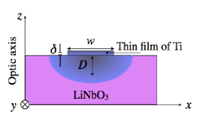
Applying a steady electric field to this structure in the -direction (along the optic axis) changes the ordinary and extraordinary refractive indices of this uniaxial (trigonal 3) material by and , respectively [17, Example 20.2-1], where is the applied voltage; is the separation between the electrodes; and and are the tensor elements of the Pockels coefficient, which have values 10.9 and 32.6 pm/V, respectively [35].
3 Modal qubits
A qubit is a pure quantum state that resides in a two-dimensional Hilbert space. It represents a coherent superposition of the basis states, generally denoted and . A qubit can be encoded in any of several degrees-of-freedom of a single photon, such as polarization [39], spatial parity [40], or the mode number of a single photon confined to a two-mode waveguide [1, 2]. The Poincaré sphere provides a geometrical representation for the state of a modal qubit, much as it does for polarization [17, Sec. 6.1A] and spatial parity [41].
Indeed, polarization offers an intrinsically binary basis and is often used to realize a qubit. However, the spatial modes of a photon in a two-mode waveguide, one of which is even and the other odd, are also binary and can therefore also be used to represent a qubit. Modal qubits are particularly suited to photonic quantum circuits since they can be both generated and easily transformed on-chip by making use of elements such as mode analyzers, mode rotators, and two-mode electro-optic directional couplers. The modal space of a two-mode waveguide therefore offers an appealing alternative to polarization for representing qubits in quantum photonic circuits.
The comparison between modal and spatial-parity qubits is instructive. Spatial-parity qubits are defined on a 2D Hilbert space in which the 1D transverse spatial modes of the photon are decomposed into even and odd spatial-parity components [40, 41, 42]. Modal qubits also relate to parity, but in a simpler way. They are defined on a 2D Hilbert space in which the bases are a single 1D even-parity function and a single 1D odd-parity function. These two functions are the fundamental (even, ) and first-order order (odd, ) transverse spatial eigenmodes of the Helmholtz equation for a two-mode waveguide.
Photon pairs can be exploited for use in quantum photonic circuits [8, 2], as well as for producing heralded single-photon pure states [43] in well-defined spatiotemporal modes, which are required for many quantum information technology applications such as quantum cryptography [44] and linear optical quantum computing [30]. Care must be taken, however, to ensure that the intrinsic quantum correlations between the twin photons are eliminated so that the surviving photon is in a pure state [45, 46, 47]. One way of achieving this is to generate the twin photons with a factorable joint amplitude [48, 49, 50, 51]. We have previously shown that a Type-0 interaction could be used to generate photon pairs that are degenerate in frequency and polarization, but with opposite mode number [2, Sec. 3]. Coupling these photons into two single-mode waveguides would allow one of these photons to be used to herald the arrival of the other. The heralded photon could then be coupled into a two-mode waveguide which, with the addition of a mode rotator, would serve as a source of modal qubits. Such a source would be analogous to the one fashioned from bulk optics by Fiorentino et al. [31] using Type-II SPDC. However, the Type-0 source of modal qubits described above would be on-chip and would also make use of the strongest nonlinear component of the second-order tensor, , thereby enhancing the efficiency of the interaction [52].
The quantum state of a single photon in a two-mode waveguide, assuming that its polarization is TE or TM, can be expressed as , where and represent the even and odd basis states, respectively; and and are their weights. All operations on the single-photon state are effected via auxiliary adjacent waveguides, which are sometimes single-mode and sometimes two-mode. We exploit the concepts of selective and controllable coupling between waveguides, together with the isomorphism between waveguide coupling and the SO(2) rotation matrix, to design a mode analyzer, a mode rotator, modal Pauli spin operators, and a CNOT gate useful for quantum information processing.
4 Mode coupling between adjacent waveguides
The coupling between two lossless, single-mode waveguides is described by a unitary matrix that takes the form [17, Sec. 8.5B]
| (1) |
where and . Here, is the phase mismatch per unit length between the two coupled modes; is the coupling interaction length; is the coupling coefficient, which depends on the widths of the waveguides and their separation as well as on the mode profiles; ; and the symbol ∗ represents complex conjugation.
This unitary matrix can equivalently be written in polar notation as [53]
| (2) |
where ; ; and . Using this representation, the coupling between the two waveguides can be regarded as a cascade of three processes: 1) phase retardation, 2) rotation, and 3) phase retardation. This becomes apparent if Eq. (2) is rewritten as
| (3) |
with
| (4) |
where ; ; and , , and represent, in consecutive order, phase retardation, rotation, and phase retardation. The phase shift is a constant of no consequence.
For perfect phase matching between the coupled modes, i.e., for and an interaction coupling length , where is an odd positive integer, the coupling matrix reduces to
| (5) |
indicating that the modes are flipped. Applying this operation twice serves to double flip the vector, thereby reproducing the input, but with a phase shift twice that of On the other hand, for , with an integer, the matrix becomes
| (6) |
Finally, for weak coupling , we have , whereupon reduces to the identity matrix.
Our interest is in three scenarios: 1) coupling between a pair of single-mode waveguides (SMWs); 2) coupling between a pair of two-mode waveguides (TMWs); and 3) coupling between a SMW and a TMW. The matrix described in Eq. (2) is not adequate for describing the coupling in the latter two cases; in general, a matrix is clearly required for describing the coupling between two TMWs. However, for the particular cases of interest here, the coupling between the two waveguides is such that only a single mode in each waveguide participates; this is because the phase-matching conditions between the interacting modes are either satisfied — or not satisfied. As an example for identical waveguides, similar modes couple whereas dissimilar modes fail to couple as a result of the large phase mismatch. The net result is that, for the cases at hand, the general matrix described in Eq. (2) reduces to submatrices of size , each characterizing the coupling between a pair of modes.
5 Mode analyzer and modal Pauli spin operator
A mode analyzer is a device that separates the even and odd components of an incoming state into two separate spatial paths. It is similar to the parity analyzer of one-photon parity space [40]. For the problem at hand, its operating principle is based on the selective coupling between adjacent waveguides of different widths. The even and odd modes of a TMW of width are characterized by different propagation constants. An auxiliary SMW (with appropriate width , length , and separation distance from the TMW) can be used to extract only the odd component [2]. The result is a mode analyzer that separates the components of the incoming state, delivering the the odd mode as an even distribution, as shown in Fig. 2(a). The end of the SMW is attached to an -bend waveguide, with initial and final widths , to obviate the possibility of further unwanted coupling to the TMW and to provide a well-separated output port for the extracted mode. If it is desired that the output be delivered as an odd distribution instead, another SMW to TMW coupling region (with the same parameters) may be arranged at the output end of the -bend, as illustrated in Fig. 2(b). This allows the propagating even mode in the SMW to couple to the odd mode of the second TMW, thereby delivering an odd distribution at the output. The appropriate coupler configuration is determined by the application at hand. It is important to note that the mode analyzer is a bidirectional device: it can be regarded as a mode combiner when operated in the reverse direction, as we will soon see.

The Pauli spin (or spatial-parity) operator introduces a phase shift of (imparts a negative sign) to the odd component of the photon state, leaving the even component unchanged; it thus acts as a half-wave retarder in mode space. It can be implemented by exploiting modal dispersion between the even and odd modes: a single TMW of length , where and are the propagation constants of the even and odd modes, respectively, results in the desired phase shift of . For a weakly dispersive medium, however, a waveguide longer than practicable might be required. An alternative approach for implementing the Pauli spin operator involves cascading a mode analyzer and a mode combiner, as illustrated in Fig. 2(c). As established in Eq. (5), perfect coupling between a pair of adjacent waveguides over an interaction length introduces a phase shift of , where is an odd positive integer. A cascade of two such couplings thus results in a phase shift , with odd, thereby implementing the Pauli spin operator . Proper design dictates that , where and are the distances traveled by the even and odd modes, respectively. Imperfections in the fabrication of the circuit may be compensated by making use of an electro-optic (EO) phase modulator, as sketched in Fig. 2(c).
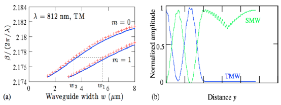
An example illustrating the operation of a mode analyzer, such as that shown in Fig. 2(a), is provided in Fig. 3. The behavior of the normalized propagation constants of the even () and odd () modes before Ti indiffusion, as a function of the waveguide width , is presented in Fig. 3(a) for TM polarization at a wavelength of m. The horizontal dotted line crossing the two curves represents the phase-matching condition for an even and an odd mode in two waveguides of different widths. The simulation presented in Fig. 3(b) displays the evolution of the normalized amplitudes of the two interacting modes with distance.
6 Mode rotator and modal Pauli spin operator
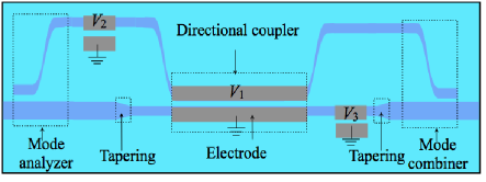
The mode rotator is an operator that rotates the state by an angle in mode space, just as a polarization rotator rotates the polarization state. It is also analogous to the parity rotator of one-photon spatial-parity space [40]. It achieves rotation by cascading a mode analyzer, a directional coupler, and a mode combiner; the three devices are regulated by separate EO phase modulators to which external voltages are applied. The mode analyzer splits the incoming one-photon state into its even and odd projections; the directional coupler mixes them; and the mode combiner recombines them into a single output.
Implementation of the mode rotator is simplified by making use of the factorization property of the unitary matrix that characterizes mode coupling in two adjacent waveguides (see Sec. 4). As shown in Eqs. (3) and (4), the coupling between two lossless waveguides can be regarded as a cascade of three stages: phase retardation, rotation, and phase retardation. If the phase-retardation components were eliminated, only pure rotation, characterized by the SO(2) operator, would remain.
The phase-retardation components can indeed be compensated by making use of a pair of EO phase modulators to introduce phase shifts of and , before and after the EO directional coupler, respectively. These simple U(1) transformations convert and in Eq. (4) into identity matrices, whereupon Eq. (3) becomes the SO(2) rotation operator. For a mode of wavelength , and an EO phase modulator of length and distance between the electrodes, the voltage required to introduce a phase shift of is , where the Pockels coefficient assumes the values and , for and , respectively [17, Sec. 20.1B].
The standard EO directional coupler consists of two adjacent identical SMWs and makes use of an EO phase modulator to control the transfer of modal power between them [17, Sec. 20.1D]. When no voltage is applied to the EO modulator, the optical power is totally transferred from one waveguide to the other, provided that the interaction length over which they interact is an odd integer multiple of the coupling length, [17, Sec. 8.5B]. The application of a voltage to the EO modulator introduces a phase mismatch between the two interacting modes that results in partial, rather than full, optical power transfer. In particular, if the voltage is chosen such that (or , then no power is transferred between the two waveguides. The voltage required to introduce a phase mismatch of is approximately [17, Sec. 20.1D]. The waveguide beam combiner suggested by Buhl and Alferness [53] operates on the same principle.
However, because our modal state resides in a TMW, rather than in a SMW associated with the usual directional coupler, a mode analyzer with a configuration similar to that shown in Fig. 2(a) is used to direct the odd component to one arm of the EO directional coupler, and the even component to the other arm through an adiabatically tapered region, as shown in Fig. 4. A mirror-image tapered region and mode combiner follow the directional coupler to recombine the two components at the output of the device. Voltages , , and are applied to the EO directional coupler, the input EO phase modulator, and the output EO phase modulator, respectively. The voltages and can be modified as necessary to ensure that the overall phases acquired by the odd and even modes, both before and after the directional coupler, are identical when .
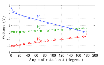
An example showing the operating voltages , and required to obtain a specified angle of rotation is provided in Fig. 5. The directional-coupler voltage has an initial value (for ) that corresponds to a phase mismatch ; decreasing results in increasing . When , the angle of rotation is ; the device then acts as the Pauli spin operator , which is a mode flipper (analogous to the parity flipper [40, 41]). For , there are an infinite number of solutions for the values of and , provided, however, that .
7 Controlled-NOT (CNOT) gate
Deterministic quantum computation that involves several degrees-of-freedom of a single photon for encoding multiple qubits is not scalable inasmuch as it requires resources that grow exponentially [31]. Nevertheless, few-qubit quantum processing can be implemented by exploiting multiple-qubit encoding on single photons [54]. We propose a novel deterministic, two-qubit, single-photon, CNOT gate, implemented as a Ti:LiNbO3 photonic quantum circuit, in which the polarization and mode number of a single photon serve as the control and target qubits, respectively.
The operation of this gate is implemented via a polarization-sensitive, two-mode, electro-optic directional coupler, comprising a pair of identical TMWs integrated with an electro-optic phase modulator, and sandwiched between a mode analyzer and a mode combiner. It relies on the polarization sensitivity of the Pockels coefficients in LiNbO3. A sketch of the circuit is provided in Fig. 6. The mode analyzer spatially separates the even and odd components of the state for a TM-polarized photon, sending the even component to one of the TMWs and the odd component to the other. At a certain value of the EO phase-modulator voltage, as explained below, the even and odd modes can exchange power. The modified even and odd components are then brought together by the mode combiner.
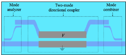
To show that the device portrayed in Fig. 6 operates as a CNOT gate, we first demonstrate that the target qubit is indeed flipped by a TM-polarized control qubit, so that . The polarization sensitivity of the Ti:LiNbO3 TMWs resides in the values of their refractive indices , which depend on the polarizations of the incident waves and the voltage applied to its EO phase modulator; and on their Pockels coefficients , which depend on the polarization [17, Example 20.2-1]. For a photon with TM polarization, the two-mode EO directional coupler offers two operating regions with markedly different properties. At low (or no) applied voltage, interaction and power transfer take place only between like-parity modes in the two waveguides because the propagation constants of the even and odd modes are different, so they are not phase-matched. However, at a particular higher value of the applied voltage, the behavior of the device changes in such a way that only the even mode in one waveguide, and the odd mode in the other, can interact and exchange power. This arises because the refractive indices of the two waveguides depend on the voltage applied to the device; they move in opposite directions as the voltage increases since the electric-field lines go downward in one waveguide and upward in the other. Figure 7 provides an example illustrating the dependencies of the propagation constants of the even and odd modes, in the two TMWs, as a function of the applied voltage.
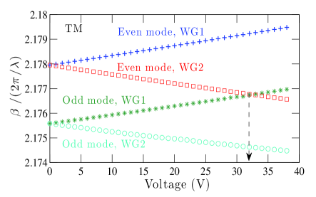
At a voltage indicated by the vertical dashed line in Fig. 7, the even mode in one waveguide is phase-matched to the odd mode in the other. In a directional coupler with suitable parameters, a TM-polarized control bit will then result in a flip of the modal bit, whereupon . A TE-polarized control qubit, on the other hand, which sees rather than , will leave the target qubit unchanged because of phase mismatch, so that . Hence, the target qubit is flipped if and only if the control qubit is , and is left unchanged if the control qubit is , so that the device portrayed in Fig. 6 does indeed behave as a CNOT gate. In principle, it would also be possible to use a TE-polarized control qubit to flip the target bit; this option was not selected because it would require a higher value of EO phase-modulator voltage since the TE Pockels coefficient is smaller than the TM Pockels coefficient [35].
A drawback of the photonic circuit illustrated in Fig. 6 is that it suffers from the effects of dispersion, which is deleterious to the operation of circuits used for many quantum information applications. Dispersion results from the dependence of the propagation constant on frequency, mode number, and polarization. Polarization-mode dispersion generally outweighs the other contributions, especially in a birefringent material such as LiNbO3.
Fortunately, however, it is possible to construct a photonic circuit in which the phase shifts introduced by dispersion can be equalized. A Ti:LiNbO3 photonic quantum circuit that behaves as a novel dispersion-managed, deterministic, two-qubit, single-photon, CNOT gate is sketched in Fig. 8. It makes use of three paths (upper, middle, and lower), in which the path-lengths of the three arms are carefully adjusted to allow for dispersion management. The third path provides the additional degree-of-freedom that enables the optical path-lengths to be equalized.
The design relies on the use of polarization-dependent mode analyzers at the input to the circuit. The TM-mode analyzer couples the odd-TM component of the state to the upper path, while the TE-mode analyzer couples the odd-TE component to the lower path. The even-TM and even-TE components continue along the middle path. Polarization-dependent mode combiners are used at the output of the circuit.
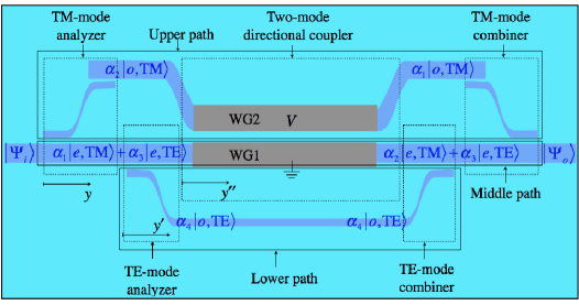
If the control qubit is in a superposition state, the general quantum state at the input to the circuit, which resides in a 4D Hilbert space (2D for polarization and 2D for mode number), is expressed as
| (7) |
where and are the basis states of the modal subspace; and are the basis states of the polarization subspace; the ’s represent the basis weights; and indicates the tensor product. Since the target (modal) qubit is flipped by a TM control qubit, the output state becomes
| (8) |
where it is clear that the two terms in the input state, and , are converted to and , respectively, at the output, exemplifying the operation of this CNOT gate. Figure 8 displays the paths taken by the components of the input state provided in Eq. (7); the output state set forth in Eq. (8) is also indicated.
The output state in Eq. (8) is entangled in polarization and mode number; it is inseparable and cannot be written in factorizable form. A particular property of the CNOT gate is the induction of entanglement between factorized qubits: if the control qubit is in the superposition state , and the target qubit is in one of the computational basis states, then the output state of the CNOT gate is maximally entangled. An experimental test of the entanglement created between the polarization and modal degrees-of-freedom can be effected by using quantum-state tomography. The input to the CNOT gate can be readily generated from a product state, say , by rotation using a waveguide-based EO TETM mode converter [55, 23], in addition to a phase modulator, as described in Sec. 6.
It remains to demonstrate the manner in which dispersion management can be achieved in the CNOT gate displayed in Fig. 8. The phase shift acquired by each component at the output is given by
| (9) |
where the ’s are the mode propagation constants; is the propagation constant of either the TM-even mode in WG1 or the TM-odd mode in WG2; is the propagation constant of the TE-even mode in WG1; , , and are odd positive integers that depend on the lengths of the TM-mode analyzer, directional coupler, and TE-mode analyzer, respectively; is the length of the directional-coupler electrode; is the path-length for the even modes before and after the directional coupler, is the path-length for the odd-TM mode before and after the directional coupler; and , , and are the overall physical lengths of the middle, upper, and lower paths, respectively. The phase shift arises from the coupling that affects the odd-TE component as it travels through the TM-mode analyzer. Phase shifts that accrue for the even modes as they pass through the mode analyzers and mode combiners are neglected because of large phase mismatches and weak coupling coefficients. By adjusting the lengths , , and , we can equalize the phase shifts encountered by each component of the state. Imperfections in the fabrication of the circuit may be compensated by making use of EO phase modulators.
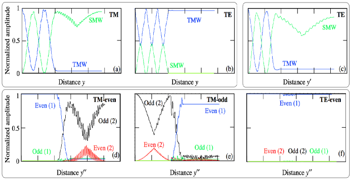
A simulation that demonstrates the performance of the polarization-dependent mode analyzers and EO TMW directional coupler is presented in Fig. 9. The lengths , , and are assumed to be adjusted such that they equalize the phase shifts encountered by each component of the state so that dispersion is not an issue. The spatial evolution of the normalized amplitudes of the odd and even modes inside the TM-mode analyzer, for TM- and TE-polarization, are displayed in Figs. 9(a) and 9(b), respectively. It is apparent that the TM-mode analyzer extracts only the TM-odd component, while the TE-odd component remains in the TMW waveguide until it couples to the lower path via the TE-mode analyzer [see Fig. 9(c)]. Figures 9(d), (e), and (f) display the performance of the directional coupler for modal inputs that are TM-even, TM-odd, and TE-even, respectively. It is apparent in Fig. 9(d) that the power in the even mode in WG1 is transferred to the odd mode in WG2 for TM polarization. Figure 9(e) reveals complementary behavior: the power in the odd mode in WG2 is transferred to the even mode in WG1. Figure 9(f), on the other hand, shows that the TE-even mode travels through the directional coupler with essentially no interaction. Figures 9(d), (e), and (f), taken together, along with the observation that the TE-odd mode preserves its modal profile during propagation, demonstrate a flip of the modal target qubit by the TM-polarized control qubit, and no flip by a TE-polarized control qubit, confirming that the photonic circuit in Fig. 8 behaves as a CNOT gate.
The absence of a total power transfer from one waveguide to another in Figs. 9(d) and 9(e) can be ascribed to sub-optimal simulation parameters. The conversion efficiency can be expected to improve upon: 1) optimizing the length of the two-mode directional coupler; 2) minimizing bending losses by increasing the length of the -bend; 3) mitigating the residual phase mismatch by more careful adjustment of the voltage; and 4) improving numerical accuracy. Moreover, the deleterious effects of dc drift and temperature on the operating voltage and stability of the two-mode directional coupler can be minimized by biasing it via electronic feedback [56]; a novel technique based on inverting the domain of one of its arms can also be used to reduce the required operating voltage [57]. Finally, it is worthy of note that decoherence associated with the use of a cascade of CNOT gates, such as might be encountered in carrying out certain quantum algorithms, may be mitigated by the use of either a qubit amplifier [32] or teleportation and error-correcting techniques [33].
8 Conclusion
The modes of a single photon in a two-mode Ti:LiNbO3 waveguide have been co-opted as basis states for representing the quantum state of the photon as a modal qubit. Various photonic quantum circuit designs have been presented for carrying out basic operations on modal qubits for quantum information processing applications. These include a mode analyzer, a mode rotator, and modal Pauli spin operators. We have also described the design of a deterministic, two-qubit, single-photon, CNOT gate, as well as a dispersion-managed version thereof, that rely on a single photon with both modal and polarization degrees-of-freedom in a joint 4D Hilbert space. The CNOT gate is a key element in certain sets of universal quantum logic gates. Simulations of the performance of all of these components, carried out with the help of the the commercial photonic and network design software package RSoft, provide support that they operate as intended. The design of these devices is based on selective and controllable power coupling among waveguides, the isomorphism between waveguide coupling and the SO(2) rotation matrix, and the tensor polarization properties of the Pockels coefficients in lithium niobate. The flexibility of Ti:LiNbO3 as a material for the fabrication guided-wave structures should accommodate the development of increasingly complex quantum circuits and serve to foster new architectures.
Acknowledgments
This work was supported by the Bernard M. Gordon Center for Subsurface Sensing and Imaging Systems (CenSSIS), an NSF Engineering Research Center; by a U.S. Army Research Office (ARO) Multidisciplinary University Research Initiative (MURI) Grant; and by the Boston University Photonics Center.
References
- [1] M. F. Saleh, B. E. A. Saleh, and M. C. Teich, “Modal, spectral, and polarization entanglement in guided-wave parametric down-conversion,” Phys. Rev. A 79, 053 842 (2009).
- [2] M. F. Saleh, G. Di Giuseppe, B. E. A. Saleh, and M. C. Teich, “Photonic circuits for generating modal, spectral, and polarization entanglement,” IEEE Photon. J. 2, 736–752 (2010).
- [3] M. Fiorentino, S. M. Spillane, R. G. Beausoleil, T. D. Roberts, P. Battle, and M. W. Munro, “Spontaneous parametric down-conversion in periodically poled KTP waveguides and bulk crystals,” Opt. Express 15, 7479–7488 (2007).
- [4] M. Avenhaus, M. V. Chekhova, L. A. Krivitsky, G. Leuchs, and C. Silberhorn, “Experimental verification of high spectral entanglement for pulsed waveguided spontaneous parametric down-conversion,” Phys. Rev. A 79, 043 836 (2009).
- [5] P. J. Mosley, A. Christ, A. Eckstein, and C. Silberhorn, “Direct measurement of the spatial-spectral structure of waveguided parametric down-conversion,” Phys. Rev. Lett. 103, 233 901 (2009).
- [6] T. Zhong, F. N. Wong, T. D. Roberts, and P. Battle, “High performance photon-pair source based on a fiber coupled periodically poled KTiOPO4 waveguide,” Opt. Express 17, 12 019–12 030 (2009).
- [7] J. Chen, A. J. Pearlman, A. Ling, J. Fan, and A. Migdall, “A versatile waveguide source of photon pairs for chip-scale quantum information processing,” Opt. Express 17, 6 727–6 740 (2009).
- [8] A. Politi, M. J. Cryan, J. G. Rarity, S. Yu, and J. L. O’Brien, “Silica-on-silicon waveguide quantum circuits,” Science 320, 646–649 (2008).
- [9] J. C. F. Matthews, A. Politi, A. Stefanov, and J. L. O’Brien, “Manipulation of multiphoton entanglement in waveguide quantum circuits,” Nature Photon. 3, 346–350 (2009).
- [10] C. H. Bennett and P. W. Shor, “Quantum information theory,” IEEE Trans. Inform. Theory 44, 2724–2742 (1998).
- [11] M. A. Nielsen and I. L. Chuang, Quantum Computation and Quantum Information (Cambridge University Press, Cambridge, UK, 2000).
- [12] J. L. O’Brien, A. Furusawa, and J. Vučković, “Photonic quantum technologies,” Nature Photon. 3, 687–695 (2009).
- [13] A. Politi, J. C. F. Matthews, M. G. Thompson, and J. L. O’Brien, “Integrated quantum photonics,” IEEE J. Sel. Topics Quantum Electron. 15, 1673–1684 (2009).
- [14] G. Cincotti, “Prospects on planar quantum computing,” J. Lightwave Technol. 27, 5755–5766 (2009).
- [15] T. D. Ladd, F. Jelezko, R. Laflamme, Y. Nakamura, C. Monroe, and J. L. O’Brien, “Quantum computers,” Nature 464, 45–53 (2010).
- [16] H. Nishihara, M. Haruna, and T. Suhara, Optical Integrated Circuits (McGraw–Hill, New York, 1989).
- [17] B. E. A. Saleh and M. C. Teich, Fundamentals of Photonics, 2nd ed. (Wiley, Hoboken, NJ, 2007).
- [18] A. C. Busacca, C. L. Sones, R. W. Eason, and S. Mailis, “First-order quasi-phase-matched blue light generation in surface-poled Ti:indiffused lithium niobate waveguides,” Appl. Phys. Lett. 84, 4430–4432 (2004).
- [19] Y. L. Lee, C. Jung, Y.-C. Noh, M. Park, C. Byeon, D.-K. Ko, and J. Lee, “Channel-selective wavelength conversion and tuning in periodically poled Ti:LiNbO3 waveguides,” Opt. Express 12, 2649–2655 (2004).
- [20] S. Tanzilli, H. De Riedmatten, W. Tittel, H. Zbinden, P. Baldi, M. De Micheli, D. B. Ostrowsky, and N. Gisin, “Highly efficient photon-pair source using periodically poled lithium niobate waveguide,” Electron. Lett. 37, 26–28 (2001).
- [21] H. Guillet de Chatellus, A. V. Sergienko, B. E. A. Saleh, M. C. Teich, and G. Di Giuseppe, “Non-collinear and non-degenerate polarization-entangled photon generation via concurrent type-I parametric downconversion in PPLN,” Opt. Express 14, 10 060–10 072 (2006).
- [22] R. C. Alferness and R. V. Schmidt, “Tunable optical waveguide directional coupler filter,” Appl. Phys. Lett. 33, 161–163 (1978).
- [23] R. C. Alferness, “Efficient waveguide electro-optic TETM mode converter/wavelength filter,” Appl. Phys. Lett. 36, 513–515 (1980).
- [24] J. Hukriede, D. Runde, and D. Kip, “Fabrication and application of holographic Bragg gratings in lithium niobate channel waveguides,” J. Phys. D: Appl. Phys. 36, R1–R16 (2003).
- [25] D. Runde, S. Brunken, S. Breuer, and D. Kip, “Integrated-optical add/drop multiplexer for DWDM in lithium niobate,” Appl. Phys. B: Lasers Opt. 88, 83–88 (2007).
- [26] D. Runde, S. Breuer, and D. Kip, “Mode-selective coupler for wavelength multiplexing using LiNbO3:Ti optical waveguides,” Cent. Eur. J. Phys. 6, 588–592 (2008).
- [27] R. V. Schmidt and H. Kogelnik, “Electro-optically switched coupler with stepped reversal using Ti-diffused LiNbO3 waveguides,” Appl. Phys. Lett. 28, 503–506 (1976).
- [28] H. Kogelnik and R. V. Schmidt, “Switched directional couplers with alternating ,” IEEE J. Quantum Electron. QE-12, 396–401 (1976).
- [29] D. P. DiVincenzo, “Two-bit gates are universal for quantum computation,” Phys. Rev. A 51, 1015–1022 (1995).
- [30] E. Knill, R. Laflamme, and G. J. Milburn, “A scheme for efficient quantum computation with linear optics,” Nature 409, 46–52 (2001).
- [31] M. Fiorentino and F. N. C. Wong, “Deterministic controlled-NOT gate for single-photon two-qubit quantum logic,” Phys. Rev. Lett. 93, 070 502 (2004).
- [32] N. Gisin, S. Pironio, and N. Sangouard, “Proposal for implementing device-independent quantum key distribution based on a heralded qubit amplifier,” Phys. Rev. Lett. 105, 070 501 (2010).
- [33] S. Glancy, H. M. Vasconcelos, and T. C. Ralph, “Transmission of optical coherent-state qubits,” Phys. Rev. A 70, 022 317 (2004).
- [34] D. H. Jundt, “Temperature-dependent Sellmeier equation for the index of refraction, , in congruent lithium niobate,” Opt. Lett. 22, 1553–1555 (1997).
- [35] K. K. Wong, ed., Properties of Lithium Niobate (Institution of Electrical Engineers, Stevenage, U.K., 2002).
- [36] M. D. Feit, J. A. Fleck, Jr., and L. McCaughan, “Comparison of calculated and measured performance of diffused channel-waveguide couplers,” J. Opt. Soc. Am. 73, 1296–1304 (1983).
- [37] S. K. Korotky and R. C. Alferness, “Ti:LiNbO3 integrated optic technology,” in Integrated Optical Circuits and Components: Design and Applications, L. D. Hutcheson, ed. (Marcel Dekker, New York, 1987).
- [38] G. B. Hocker and W. K. Burns, “Mode dispersion in diffused channel waveguides by the effective index method,” Appl. Opt. 16, 113–118 (1977).
- [39] C. H. Bennett and G. Brassard, “Quantum cryptography: Public key distribution and coin tossing,” in Proceedings of the International Conference on Computers, Systems & Signal Processing, pp. 175–179 (Institute of Electrical and Electronics Engineers, Bangalore, India, 1984).
- [40] A. F. Abouraddy, T. Yarnall, B. E. A. Saleh, and M. C. Teich, “Violation of Bell’s inequality with continuous spatial variables,” Phys. Rev. A 75, 052 114 (2007).
- [41] T. Yarnall, A. F. Abouraddy, B. E. A. Saleh, and M. C. Teich, “Synthesis and analysis of entangled photonic qubits in spatial-parity space,” Phys. Rev. Lett. 99, 250 502 (2007).
- [42] T. Yarnall, A. F. Abouraddy, B. E. A. Saleh, and M. C. Teich, “Experimental violation of Bell’s inequality in spatial-parity space,” Phys. Rev. Lett. 99, 170 408 (2007).
- [43] B. E. A. Saleh and M. C. Teich, “Sub-Poisson light generation by selective deletion from cascaded atomic emissions,” Optics Commun. 52, 429–432 (1985).
- [44] N. Gisin, G. Ribordy, W. Tittel, and H. Zbinden, “Quantum Cryptography,” Rev. Mod. Phys. 74, 145–195 (2002).
- [45] A. F. Abouraddy, B. E. A. Saleh, A. V. Sergienko, and M. C. Teich, “Degree of entanglement for two qubits,” Phys. Rev. A 64, 050 101 (2001).
- [46] P. J. Mosley, J. S. Lundeen, B. J. Smith, P. Wasylczyk, A. B. U’Ren, C. Silberhorn, , and I. A. Walmsley, “Heralded generation of ultrafast single photons in pure quantum states,” Phys. Rev. Lett. 100, 133 601 (2008).
- [47] Z. H. Levine, J. Fan, J. Chen, A. Ling, and A. Migdall, “Heralded, pure-state single-photon source based on a Potassium Titanyl Phosphate waveguide,” Opt. Express 18, 3708–3718 (2010).
- [48] W. P. Grice, A. B. U’Ren, and I. A. Walmsley, “Eliminating frequency and space–time correlations in multiphoton states,” Phys. Rev. A 64, 063 815 (2001).
- [49] Z. D. Walton, M. C. Booth, A. V. Sergienko, B. E. A. Saleh, and M. C. Teich, “Controllable frequency entanglement via auto-phase-matched spontaneous parametric down-conversion,” Phys. Rev. A 67, 053 810 (2003).
- [50] Z. D. Walton, A. V. Sergienko, B. E. A. Saleh, and M. C. Teich, “Generation of polarization-entangled photon pairs with arbitrary joint spectrum,” Phys. Rev. A 70, 052 317 (2004).
- [51] S. Carrasco, J. P. Torres, L. Torner, A. V. Sergienko, B. E. A. Saleh, and M. C. Teich, “Spatial-to-spectral mapping in spontaneous parametric down-conversion,” Phys. Rev. A 70, 043 817 (2004).
- [52] L. E. Myers, R. C. Eckardt, M. M. Fejer, R. L. Byer, W. R. Bosenberg, and J. W. Pierce, “Quasi-phase-matched optical parametric oscillators in bulk periodically poled LiNbO3,” J. Opt. Soc. Am. B 12, 2102–2116 (1995).
- [53] L. L. Buhl and R. C. Alferness, “Ti:LiNbO3 waveguide electro-optic beam combiner,” Opt. Lett. 12, 778–780 (1987).
- [54] Y. Mitsumori, J. A. Vaccaro, S. M. Barnett, E. Andersson, A. Hasegawa, M. Takeoka, and M. Sasaki, “Experimental demonstration of quantum source coding,” Phys. Rev. Lett. 91, 217 902 (2003).
- [55] A. Yariv, “Coupled-mode theory for guided-wave optics,” IEEE J. Quantum Electron. QE-9, 919–933 (1973).
- [56] A. Djupsjobacka and B. Lagerstrom, “Stabilization of a Ti:LiNbO3 directional coupler,” Appl. Opt. 28, 2205–2206 (1989).
- [57] F. Lucchi, D. Janner, M. Belmonte, S. Balsamo, M. Villa, S. Giurgola, P. Vergani, and V. Pruneri, “Very low voltage single drive domain inverted LiNbO3 integrated electro-optic modulator,” Opt. Express 15, 10 739–10 743 (2007).