Optical Absorption Characteristics of Silicon Nanowires for Photovoltaic Applications
Abstract
Solar cells have generated a lot of interest as a potential source of clean renewable energy for the future. However a big bottleneck in wide scale deployment of these energy sources remain the low efficiency of these conversion devices. Recently the use of nanostructures and the strategy of quantum confinement have been as a general approach towards better charge carrier generation and capture. In this article we have presented calculations on the optical characteristics of nanowires made out of silicon. Our calculations show these nanowires form excellent optoelectronic materials and may yield efficient photovoltaic devices.
Index Terms:
silicon, nanowire, solar cell, excitonI Introduction
In recent years a lot of innovation in the semiconductor industry has
enabled solar cell designs with higher conversion efficiencies though the use of inexpensive materials
and processes [1, 2]. Today III-V semiconductor based solar cells
can achieve upto 40% efficiency. Most strategies in improving the efficiencies target
improving optical absorption, and efficient collection of generated photocarriers. In recent times
improving efficiencies through quantum confinement has generated a lot of interest, with the advent of
multijunction cells (MJSCs) and quantum dot based devices [3].
However most of the high efficiency devices are still based on exotic III -V hetrostructures, which are
expensive to process and manufacture. Hence a real incentive in realizing cells made out of silicon still
exists due to the existing infrastructure already in place.
A possible candidate for the next generation of solar cells are silicon nanowires. Silicon nanowires are 1D materials
and there has been interest to incorporate them into photovoltaic cell design due to the wide availability of the material and existing processing infrastructure. The advantage of using nanowires being that, like quantum dots we
can tune the band gap to a specific part of the solar spectrum, but with the added advantage that carrier transport in the solar cell is not dependent on quantum tunneling as proposed in [4].
In this paper we have presented the optical properties of silicon nanowires of different dimensions
evaluated from ab initio calculations. Our results show that the nanowires are direct bandgap materials
and we can alter the energy gap anywhere between 2-5 eV, that gives us a wavelength selectivity from
200 to 600 nm wavelengths. Results on intrinsic absorption and excitonic binding energies are also
presented later in this article.
The rest of this paper is organised as follows, Section-II describes the computational methodology followed for the ab initio calculations, In Section -III we present our results on bandstructure and optical properties. like the dielectric function and absorption coefficient. Finally we evaluate how exciton binding energies in these nanowires vary with the length of the nanowire (corresponds to quantum confinement in the axial direction).
II Computational Methodology
In this section we describe the first principles calculations carried out for the silicon nanowires systems.
The computations were carried out using a density functional DFT-LDA approach using a parallel binary of the PWScf
distribution. We carried out computations on three nanowires. We consider the nanowires to be oriented along the [100]
plane, each having a square cross section. The dangling bonds on the surface of the nanowire are passivated by
hydrogen terminations. Before performing electronic structure calculations we subjected the unit cells to a geometry
optimization procedure.The equilibrium lattice relaxed to a unit cell with the Si-Si bond spacing to be 2.324 Å and Si-H
spacing to be 1.5 Å. The translational lattice constant for the nanowires was 5.43 Å.
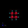
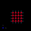
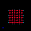
We have considered three nanowire unit cells in this paper each with a diameter 4.34 Å, 8.16 Å and
10.75 Å. These have been designated as Si11, Si22 and Si33 systems in this paper. The relaxed unit
cells considered for the calculations presented in this paper are shown in Fig. 1. The silicon atoms
in the Si11 unit cell forms the primitive cell for the Si22, Si33 nanowires as well. The SiXX
system is formed by ’X’ repetitions of this atomic arrangement in the x and y directions. Each of the atoms
in the Si11 cell occupy four different z-planes at , and .
The electronic structure of each of the nanowire unit cells was computed self consistently using a plane wave pseudopotential method. We utilized Van Barth Carr soft potentials for both silicon and hydrogen, with a Perdew Zunger exchange and correlation [5]. The SCF calculations were performed with a grid of 20 uniformly spaced k-vectors within the 1D Brilliouin Zone of the nanowires. A kinetic energy cutoff of 80 Ry was deemed sufficient for numerical convergence of total energy. For the computation of optical absorption coefficient , a Drude-Lorentz broadening of 0.13 eV has been applied.
III Electronic and Optical Characteristics
III-A Bandstructure
The silicon nanowires unlike bulk silicon are direct band gap semiconductors, which would make them excellent choices for optical applications. Authors in [6, 7, 8] have also reported direct band gaps and monotonically decreading bandgapes from their theoretical calculations.
All the nanowires exhibit exceptionally high effective masses of holes and electrons. For example the Si11 wire has a almost zero dispersion state on the top of the valence band. Similarly, the lowest conduction bands are also relatively heavy compared to their values in the bulk state. This is quite advantageous as it allows for extension of carrier lifetime as binding energy of excitons are directly dependent on it (5). We found that the energy gap of the nanowires decrease with increasing width. The wide tunability in the band gap of the nanowires allows us to tune the selectivity of optical absorption of the nanowire. The idea behind this being to match optical absorption in solar cells to the spectrum of the incoming solar radiation. A second intersting feature of the band structure is the weak dispersion of the conduction and valence bands leads to a high effective mass both in the conduction and valence bands. There is some experimental evidence [9] who have found out that carrier mobilities in intrinsic nanowires is extremely low. Table-I shows the effective masses of the lowest four conduction bands for all the three systems. Due to the relatively weak dispersion seen in these wires especially the Si11 and Si22 systems, it is prudent to present a thermally averaged effective mass, i.e. a harmonic average over a energy range from the lowest conduction band energy.
| Syst. | VB | CB | (eV) | ||
|---|---|---|---|---|---|
| Si11 | V1 | C1 | 5.165 | 1.44 | 1.48e-5 |
| Si11 | V1 | C2 | 5.272 | 1.92 | 0.0196† |
| Si11 | V1 | C3 | 5.275 | 0.58 | 0.0125† |
| Si11 | V1 | C4 | 5.61 | 0.91 | 0.5951† |
| Si11 | V2 | C1 | 5.318 | 1.44 | 0.000313 |
| Si11 | V2 | C2 | 5.425 | 1.92 | 1.63e-6 |
| Si11 | V2 | C3 | 5.428 | 0.58 | 0.11 |
| Si11 | V2 | C4 | 7.763 | 0.91 | 0.00549 |
| Si11 | V3 | C1 | 5.327 | 1.44 | 3.21e-5 |
| Si11 | V3 | C2 | 5.434 | 1.92 | 0.1759 |
| Si11 | V3 | C3 | 5.437 | 0.58 | 1.28e-4 |
| Si11 | V3 | C4 | 5.772 | 0.91 | 3.59e-6 |
| Si11 | V4 | C1 | 6.623 | 1.44 | 2.07e-5 |
| Si11 | V4 | C2 | 6.73 | 1.92 | 0.0360 |
| Si11 | V4 | C3 | 6.733 | 0.58 | 0.0209 |
| Si11 | V4 | C4 | 7.068 | 0.91 | 3.59e-6 |
| Si22 | V1 | C1 | 3.497 | 0.71 | 7.07e-7 |
| Si22 | V1 | C2 | 3.574 | 0.35 | 7.73e-7 |
| Si22 | V1 | C3 | 3.577 | 0.82 | 0.0260 |
| Si22 | V1 | C4 | 3.577 | 0.26 | 1.7e-7 |
| Si22 | V2 | C1 | 3.498 | 0.71 | 6.97e-7 |
| Si22 | V2 | C2 | 3.574 | 0.35 | 0.0004 |
| Si22 | V2 | C3 | 3.578 | 0.82 | 0 |
| Si22 | V2 | C4 | 3.578 | 0.26 | 0.0087 |
| Si22 | V3 | C1 | 3.558 | 0.71 | 6.96e-7 |
| Si22 | V3 | C2 | 3.634 | 0.35 | 0.0002 |
| Si22 | V3 | C3 | 3.638 | 0.85 | 0.0145 |
| Si22 | V3 | C4 | 3.638 | 0.26 | 0.0048 |
| Si22 | V4 | C1 | 3.69 | 0.71 | 0.204† |
| Si22 | V4 | C2 | 3.766 | 0.35 | 9.01e-7 |
| Si22 | V4 | C3 | 3.77 | 0.85 | 5.41e-5 |
| Si22 | V4 | C4 | 3.77 | 0.26 | 1.81e-5 |
| Si33 | V1 | C1 | 2.042 | 0.58 | 4.23e-10 |
| Si33 | V1 | C2 | 2.105 | 1.7 | 0 |
| Si33 | V1 | C3 | 2.116 | 0.9 | 1e-4 |
| Si33 | V1 | C4 | 2.116 | 0.81 | 0 |
| Si33 | V2 | C1 | 2.044 | 0.58 | 4.3e-10 |
| Si33 | V2 | C2 | 2.107 | 1.7 | 1e-4 |
| Si33 | V2 | C3 | 2.118 | 0.9 | 0 |
| Si33 | V2 | C4 | 2.118 | 0.81 | 7e-6 |
| Si33 | V3 | C1 | 2.179 | 0.58 | 1.13e-6 |
| Si33 | V3 | C2 | 2.242 | 1.7 | 2e-11 |
| Si33 | V3 | C3 | 2.253 | 0.9 | 3.78e-5 |
| Si33 | V3 | C4 | 2.253 | 0.81 | 9.4e-6 |
| Si33 | V4 | C1 | 2.194 | 0.58 | 0.005748† |
| Si33 | V4 | C2 | 2.257 | 1.7 | 8.89e-9 |
| Si33 | V4 | C3 | 2.268 | 0.9 | 2.03e-11 |
| Si33 | V4 | C4 | 2.268 | 0.81 | 5.6e-12 |
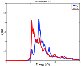
indicates a strong absorption peak in Fig. 4. Calculations for other transitions are weak and not discussed in this paper.

III-B Optical Absorption
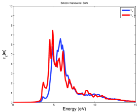
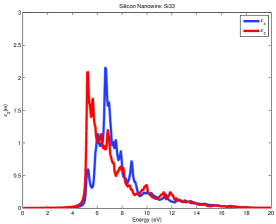
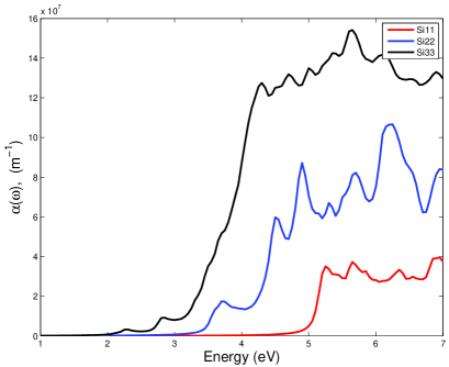
All the nanowires examined in this paper show features in the absorption spectrum the correspond to excitonic processes. A simultaneous comparison of their absorption spectra is shown in Fig. 4. The lowest excitonic peaks for each of the nanowires occur at 5.25 eV (232 nm), 3.7 eV (335 nm), and 2.3 eV (539 nm) in the increasing order of size. The corresponding optical wavelength is listed in parentheses. We see that absorption is tunable from the visible region to the near UV portion of the solar spectrum. These peaks are also quite prominent in the Si11 wire as compared to the Si33 nanowire due to the a small density of states in the conduction band. The rippled nature of the absorption spectrum weakens as the size increases. In the Si33 wire, these oscillations are almost washed out and the spectrum looks similar to that of a direct bandgap material with a exponential absoprtion edge near the conduction band energy [10, 11]. To ascertain the exact transitions that show up in the absorption spectrum, we computed the dipole matrix element of for each of the eigenvalues at and computed a quantity called the oscillator strength . The quantity is proportional to the square of the dipole matrix as
| (1) |
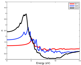
where the summation is over all possible polarizations. The magnitude of is a direct gauge of the strength of absorption at a particular energy. These numbers have been tabulated in Table-I. We observed that only a few excitations have significant values of appear optically active in the absorption spectrum. These excitations are also marked in Table-I. Other optical properties of these nanowires are also presented in Fig. 3. The strong transition peaks are more clearly visible in the plots for .
III-C Excitonic Binding energy
It is known that excitonic processes are helpful in extending lifetimes of the electron hole pairs created by optical absorption. The radiative lifetimes of an exciton is proportional to the binding energy . Hence it is useful to evaluate how change in the length of the nanowire changes the binding energy of the 1D exciton. To get this dependence we followed the methods of [12, 13] solving a two particle Schrodinger equation for an electron-hole system. In this section we have presented binding energy results for the lowest lying excitonic state in each of the nanowires. The Hamiltonian for such a system can be written in the Hartree approximation
| (2) |
The first two terms are simply the kinetic energy of the electron and hole respectively and the third term is the screened Coulomb potential. The exciton is assumed to be immersed in a surrounding medium with an effective dielectric constant . For each of the nanowires we used a value computed from the real dielectric constant at zero frequency i.e. . This Hamiltonian is diagonalized by a two particle wave function of the form
| (3) |
where is a fitting constant and N is a normalizing constant. This test wavefunction was originally applied to 1D quantum wells. This trial wavefunction is acceptable in SiNWs as it is reasonable to conceptually think of a nanowire as a 1D quantum well with an unsually long width. Equation (3) makes a single assumption that the wavefunction becomes zero at the ends of the quantum well, which is applicable to the nanowire as well. To find the binding energy of the exciton we use a variational method of minimizing the total energy over different values of . The ground state of the exciton is simply
| (4) |
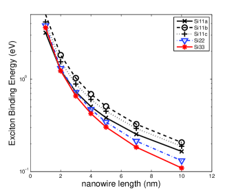
The minimized value of corresponds to the effective Bohr radius of the exciton. The binding energies have been plotted as a function of nanowire length in Fig. 5. We see that the binding energies monotonically increase as the nanowire is made shorter. This dependence is expected as the stronger confinement causes an increase in the effective mass of the charge carriers. The bulk excitonic binding energy is dependent on the reduced mass of the exciton given by the equation
| (5) |
where . We also see that the excitonic absorption is the strongest in the Si11 system compared to the shorter excitonic peaks seen in the Si22 and Si33 system (Fig. 4).Using the method presented above, we computed the exciton binding energies for the strongest transitions in the nanowire systems. There are three strong transitions of interest in the Si11 system and one transition each in the Si22 and Si33 system (see Table-I). We found that the excitons in the nanowires are predominantly Mott Wannier type. The typical Bohr radii for the 1D free exciton was found to range between 2.5-5 nm. The largest radius being exhibited by the Si33 wire due to a strong screening potential. However confining the exciton in a short nanowire, with lengths less than causes a large jump in the binding energies of the excitons as the electron hole pairs are forced to be closer to each other. The binding energies have a strong effect on the lifetime of these carriers. The radiative lifetime is related to the oscillator strength and the exciton binding energy by the relation [14, 15]
| (6) |
where , is the refractive index of the material and the other symbols have their usual meanings. We found out that these nanowires exhibit unusually large exciton lifetimes with numbers of the order of a microsecond. We have summarized our findings for a specimen length of 10 nm (see Table-II). In the Si11 wire designated Si11c the radiative lifetime is about 4 ns ( and similar vales of ), far less than the other two transitions Si11a and Si11b. This is simply because of the large oscillator strength of this excitation is also responsible for a quick decay.
| Syst. | n | (eV) | (nm) | () | |||
|---|---|---|---|---|---|---|---|
| Si11a | 1.5 | 1.2 | 0.1655 | 2.55 | 1.92 | 0.016 | 0.152 |
| Si11b | 1.5 | 1.2 | 0.2068 | 3.457 | 0.58 | 0.198 | |
| Si11c | 1.5 | 1.2 | 0.188 | 3.1 | 0.91 | 0.233 | |
| Si22 | 3 | 1.7 | 0.1314 | 4.216 | 0.71 | 0.051 | 0.022 |
| Si33 | 5 | 2.4 | 0.1095 | 5.08 | 0.58 | 0.955 |
IV Conclusion
We have presented first principles calculations for silicon nanowires for potential applications in photovoltaic applications. Results indicate that the nanowires are direct band gap semiconductors and show excellent wavelength selectivity in the optical region of the solar spectrum. We also identified the optically active interband transitions present in these nanowires and used it to calculate excitonic effects in the nanowire by solving a two particle Schrodinger equation. Our calculations indicate that excitons in these nanowires show large radiative lifetimes of the order of several microseconds for nanowires as small as 10 nm in length. This number is expected to grow significantly with further confinement as we move into the quantum dot regime.
References
- [1] A. Luque and A. Martí, “Increasing the efficiency of ideal solar cells by photon induced transitions at intermediate levels,” Phys. Rev. Lett., vol. 78, pp. 5014–5017, Jun 1997.
- [2] M. R. Lee, R. D. Eckert, K. Forberich, G. Dennler, C. J. Brabec, and R. A. Gaudiana, “Solar power wires based on organic photovoltaic materials,” Science, vol. 324, pp. 232–235, April 2009.
- [3] S. M. Hubbard, C. Bailey, S. Polly, C. Cress, J. Andersen, D. Forbes, and R. Raffaelle, “Nanostructured photovoltaics for space power,” Journal of Nanophotonics, vol. 3, p. 031880, 2009.
- [4] G. Conibeer, M. Green, E.-C. Cho, D. König, Y.-H. Cho, T. Fangsuwannarak, G. Scardera, E. Pink, Y. Huang, T. Puzzer, S. Huang, D. Song, C. Flynn, S. Park, X. Hao, and D. Mansfield, “Silicon quantum dot nanostructures for tandem photovoltaic cells,” Thin Solid Films, vol. 516, no. 20, pp. 6748 – 6756, 2008. Proceedings on Advanced Materials and Concepts for Photovoltaics EMRS 2007 Conference, Strasbourg, France.
- [5] J. P. Perdew and A. Zunger, “Self-interaction correction to density-functional approximations for many-electron systems,” Phys. Rev. B, vol. 23, pp. 5048–5079, May 1981.
- [6] G. Sanders and Y. C. Chang, “Theory of optical properties of quantum wires in porous silicon,” Phy. Rev. B, vol. 45, Apr 1992.
- [7] A. Miranda, R. Vázquez, A. Díaz-Méndez, and M. Cruz-Irisson, “Optical matrix elements in tight-binding approach of hydrogenated si nanowires,” Microelectronics Journal, vol. 40, no. 3, pp. 456–458, 2009. Workshop of Recent Advances on Low Dimensional Structures and Devices (WRA-LDSD).
- [8] M. Bruno, M. Palummo, S. Ossicini, and R. D. Sole, “First-principles optical properties of silicon and germanium nanowires,” Surface Science, vol. 601, no. 13, pp. 2707 – 2711, 2007. International Conference on NANO-Structures Self-Assembling, International Conference on NANO-Structures Self-Assembling.
- [9] Y. Cui, X. Duan, J. Hu, and C. M. Lieber, “Doping and electrical transport in silicon nanowires,” The Journal of Physical Chemistry B, vol. 104, no. 22, pp. 5213–5216, 2000.
- [10] A. Poruba, J. Springer, L. Mullerova, A. Beitlerova, M. Vanecek, N. Wyrsch, and A. Shah, “Temperature dependence of the optical absorption coefficient of microcrystalline silicon,” Journal of Non-Crystalline Solids, vol. 338-340, pp. 222 – 227, 2004. Proceedings of the 20th International Conference on Amorphous and Microcrystalline Semiconductors.
- [11] P. M. Derlett, T. C. Choy, and A. M. Stoneham, “An investigation of the porous silicon optical absorption power law near the band edge,” Journal of Physics: Condensed Matter, vol. 7, no. 12, p. 2507, 1995.
- [12] G. Bastard, E. E. Mendez, L. L. Chang, and L. Esaki, “Exciton binding energy in quantum wells,” Phys. Rev. B, vol. 26, pp. 1974–1979, Aug 1982.
- [13] B. Gerlach, J. Wüsthoff, M. O. Dzero, and M. A. Smondyrev, “Exciton binding energy in a quantum well,” Phys. Rev. B, vol. 58, pp. 10568–10577, Oct 1998.
- [14] V. Perebeinos, J. Tersoff, and P. Avouris, “Radiative lifetime of excitons in carbon nanotubes,” Nano Letters, vol. 5, pp. 2495–2499, December 2005.
- [15] F. Seitz and D. Turnbull, Solid state physics advances in research and applications, vol. 15. Academic Press, 1963.
| Vidur Parkash received his B.E (Hons.) degree in Electronics and Communication Engineering from Maharshi Dayanand University, India in 2004. He is currently working towards his Ph.D. degree in Electrical Engineering at Michigan Technological University. His research interests include computational nanoelectronics, optoelectronic devices and VLSI design. |
| Anand K Kulkarni received his B.Sc. and M.Sc. degrees in Physics from Karnatak University, Dharawad, India in 1967 and 1970 respectively. He obtained M.S. in Physics(Solid State Physics) from Iowa State University, Ames, Iowa in 1975 and Ph.D. in Engineering(Electrical) from University of Nebraska , Lincoln, Nebraska in 1979. He joined Michigan Technological University, Houghton, MI in 1978 as a visiting instructor and is currently an associate professor in the department of Electrical and Computer Engineering. His research interests are in electronic and photonic materials and devices. |