Large low-frequency resistance noise in chemical vapor deposited graphene
Abstract
We report a detailed investigation of resistance noise in single layer graphene films on Si/SiO2 substrates obtained by chemical vapor deposition (CVD) on copper foils. We find that noise in these systems to be rather large, and when expressed in the form of phenomenological Hooge equation, it corresponds to Hooge parameter as large as . We also find the variation in the noise magnitude with the gate voltage (or carrier density) and temperature to be surprisingly weak, which is also unlike the behavior of noise in other forms of graphene, in particular those from exfoliation.
The electronic properties of graphene has recently been the subject of intense research for both fundamental science and technological applications. Mechanically exfoliated graphene offers the cleanest devices with mobility in the range of cm2/Vs suspended_Kim ; suspended_andrei , forming the backbone of fundamental phenomena such as the fractional quantum Hall effect FQHE_andrei ; FQHE_kim , or ultra-high frequency transistors 50GhZ_graphene . The exfoliation process is however statistical, and for regular large scale production, several new methods have been suggested including epitaxial growth of graphene on SiC wafers SiC_1 ; SiC_2 , reduction of graphene oxide graphite_oxide , and thermally grown graphene from decomposition of hydrocarbon (methane) on transition metal (copper, nickel, iridium etc.) surfaces CVD_Nature ; CVD_science ; CVD_1 ; CVD_2 ; CVD_4 ; CVD_5 ; CVD_6 ; CVD_Park ; APL_QHE . The latter metal-based chemical vapor deposition (CVD) technique of realizing large area graphene is of particular interest as it displays excellent electrical (high mobility CVD_science , low resistance/square, half-integer quantum Hall effect APL_QHE ), mechanical (large gauge factor and electromechanical stability CVD_Nature ) and optical (high transmittance CVD_5 ) properties. Moreover, recent developments in transferring large films of single-layer CVD-graphene onto insulating substrates offer great promise in nanoelectronics, transparent electrodes in solar photovoltaics CVD_5 , or flexible/stretchable electronic applications CVD_6 . An important aspect of such applications is the intrinsic electrical noise in CVD-graphene films, which has not been explored so far. A study of electrical noise may also be crucial in understanding the nature of disorder in these materials which can be significantly different from the other forms of graphene atin_prl ; atin_apl . In this letter we report the first experimental investigation of low-frequency fluctuations of electrical resistance, often known as the -noise or flicker noise, in large-area films of single layer graphene (SLG) grown on Cu-foil and subsequently transferred onto Si/SiO2 substrate. We find the noise in CVD-graphene to be significantly larger than typical exfoliated graphene devices, along with several surprising features that separates the kinetics of disorder in CVD graphene from other graphene systems.

Recent studies of carrier mobility () Avouris_PRB and noise Avouris ; atin_prl ; atin_apl in exfoliated graphene on insulating substrates indicates that both static (that gives rise to average resistivity) and time varying (resulting in noise) components of disorder are dominated by the trapped charges at the graphene-substrate interface. This is particularly true at low carrier density () where scattering off the Coulomb potential from the trapped charges leads to a linear dependence of graphene conductivity () sdsarma_BLG . Short range scattering, involving for examples lattice defects or neutral impurities etc, become important only at large where the Coulomb potentials are largely screened. In CVD-graphene the situation can be very different. The process of etching of the host metal, mechanical stressing during the transfer process etc., have been shown to lead to considerable additional disorder, which manifests in lower , and often a clearly visible D-peak in Raman spectroscopy CVD_Park . Indeed, low temperature magnetoresistance measurements in CVD-graphene reveal a short elastic intra-valley mean free path, indicating presence of spatially extended defects, such as line defects, dislocations and ripples APL_QHE . Whether this additional disorder can also cause higher noise in CVD-graphene is not known.

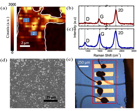
The CVD-graphene used in our experiments was grown by decomposition of ethylene on Cu foils at 875 0C as described in Ref [13]. Then a polymethyl methacrylate (PMMA) layer was spun on top of the graphene layer formed on the Cu foil, and the Cu foil was then dissolved in 1 M iron chloride. The remaining graphene/PMMA layer was thoroughly washed with deionized water and transferred to a Si/SiO2 substrate. Subsequently, the PMMA was dissolved in hot acetone (80 0C) for one hour. The heavily doped silicon was used as backgate. Following transfer to the Si/SiO2 substrate a detailed Raman spectroscopy was carried out on all our systems. Fig. 1 shows a map of the D-peak ( cm-1) intensity from a typical section of our CVD-graphene (Fig. 1a), and two representative spectra (Fig. 1c,d), which indicates a spatially varying ratio ( and are intensities of the 2D and G bands respectively). Both features can arise from a spatially non-uniform adhesion/interaction of graphene with the underlying substrate, and associated ripples/local ruptures/line defects/residual byproducts of Cu etching process etc., highlighting significant disorder of non-Coulombic origin APL_QHE . However, the 2D peaks could be described with a single Lorentzian line-shape, confirming single-layer graphene. An electrically contacted (with Au metal pads) device is shown in Fig. 1d, where a five-probe geometry was used to measure the -noise in a dynamically balanced Wheatstone bridge configuration. Both standard time-averaged resistance (utilizing four of the contacts) and noise were measured in low-frequency ac constant current mode. A detail description of the experimental methods are available elsewhere atin_prl ; atin_apl . In order to avoid gate leakage-related problems we restricted most measurements at temperature K.

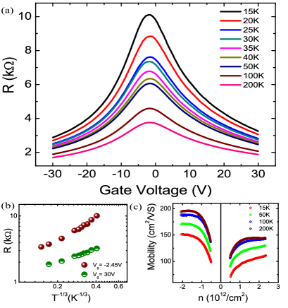
The resistance ()backgate voltage () trace of the device in Fig 1d is shown in Fig. 2a for various values of ranging from 15 K to 200 K. The sheet resistance was found to be /sq at room temperature. The Dirac point was found to be low, which we believe to be a combined effect of substrate doping and surface adsorption. was found to increase sharply with decreasing at all , reminiscent of the same in ozonization-damaged exfoliated graphene Ozonization . The -dependence of also seems to indicate a Mott-type variable range hopping with (see Fig. 2b), although limited range in or can make such an analysis relatively inaccurate.
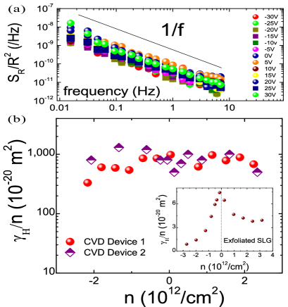
The noise measurements were performed as function of and . In Fig. 3a we show the power spectral density (PSD), , of noise over nearly three decades of frequency at various for K. The PSD can be normalized with Hooge’s phenomenological equation:
| (1) |
where is the Hooge parameter, is the area of graphene between the voltage probes, and is the spectral exponent. In all cases we find , indicating a -type spectrum, and hence, a wide distribution of time scales in the kinetics of disorder. The noise amplitude, defined as , was found to be essentially independent of (or ) in both electron and hole-doped regimes. Different devices showed identical behavior as illustrated in Fig. 3b. This weak variation in noise, found for all down to 15 K, is in contrast to the -dependence of the noise amplitude in exfoliated single layer graphene, where decreases rapidly with increasing on both sides of the Dirac point (see inset of Fig. 3b) atin_apl .

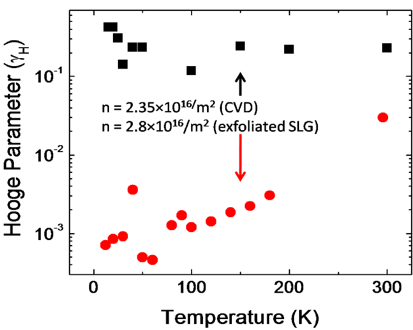
Another crucial aspect to note is that the absolute magnitude of is nearly hundred times larger in CVD-graphene in comparison to the exfoliated devices in the same range of . This is highlighted in Fig. 4, where we show the -variation of (at cm-2) for both graphene systems. For CVD-graphene is not only independent of between K, but also displays a that is about one to two orders of magnitude higher than most graphene based systems atin_prl ; atin_apl . The difference appears even larger at lower T, where noise level in exfoliated (or epitaxial) graphene are significantly reduced.
A possible explanation to the weak variation of noise in CVD-graphene can be through the mechanism of correlated number and mobility fluctuations due to the trap states at the graphene-substrate interface Atin_unpublished ; correlated model_jayaraman . Such a mechanism predicts due to number fluctuations, and , when mobility fluctuation dominates. In Fig. 2c, we show that the indeed varies weakly with in our devices, possibly indicating mobility fluctuations to be the dominant source of noise. However, similar substrates have been used for exfoliated graphene that showed much lower noise magnitude atin_apl . In our CVD graphene, migration of surface adsorbates, such as those incurred during the transfer process, or relaxation of structural defects due to the in-built stress may lead to large noise magnitude.These processes lead to mobility fluctuations, which in an inhomogeneous charge distribution may lead to a gate voltage (as well as temperature)-independent noise. In the inhomogeneous regime, which can persist upto large in highly disordered CVD graphene, the gate voltage is likely to affect relative number of electron and hole puddles rather than the charge density within a particular puddle significantly martin .
In conclusion, we report experimental investigation of resistance noise in single layer chemical vapor deposited graphene transferred onto a Si/SiO2 substrate. We find the noise magnitude to be nearly two orders of magnitude larger than exfoliated single graphene, and largely independent of temperature and carrier density. A substrate or surface trap-mediated fluctuation model seems likely, although several details of the noise behavior remains to be understood quantitatively.
Acknowledgement We acknowledge the Department of Science and Technology (DST) for a funded project, and Indo-US Science and Technology Forum (IUSSTF) for support. ANP thanks CSIR for financial support.
References
- (1) K.I. Bolotin, K.J. Sikes, Z. Jiang, M. Klima, G. Fudenberg, J. Hone, P. Kim, and H.L. Stormer, Solid State Commun. 146, 351 (2008).
- (2) X. Du, I. Skachko, A. Barker, and E. Y. Andrei, Nature Nanotech. 3, 491 (2008).
- (3) X. Du, I. Skachko, F. Duerr, A. Luican, and E. Y. Andrei, Nature 462, 192 (2009).
- (4) K. I. Bolotin, F. Ghahari, M. D. Shulman, H. L. Stormer, and P. Kim1, Nature 462, 196 (2009).
- (5) F. Xia, T. Mueller, Y. Lin, A. Valdes-Garcia, and P. Avouris, Nature Nanotech. 4, 839 (2009).
- (6) W. A. de Heer, C. Berger, X. Wu, P. N. First, E. H. Conrad, X. Li, T. Li, M. Sprinkle, J. Hass, M. L. Sadowski, M. Potemski, and G. Martinez, Solid State Commun. 143, 92 (2007).
- (7) K. V. Emtsev, A. Bostwick, K. Horn, J. Jobst, G. L. Kellogg, L. Ley, J. L. McChesney, T. Ohta, S. A. Reshanov, J. R hrl, E. Rotenberg, A. K. Schmid, D. Waldmann, H. B. Weber, and T. Seyller, Nature Mater. 8, 203 (2009).
- (8) S. Gilje, S. Han, M. Wang, K. L. Wang, and R. B. Kaner, Nano Lett. 7, 3394 (2007).
- (9) Q. K. Yu, J. Lian, S. Siripongert, H. Li, Y. P. Chen, and S. S. Pei, Appl. Phys. Lett. 93, 113103 (2008).
- (10) A. Reina, X. Jia, J. Ho, D. Nezich, H. Son, V. Bulovic, M. S. Dresselhaus, and J. Kong, Nano Lett. 9, 30 (2009).
- (11) K. S. Kim, Y. Zhao, H. Jang, S. Y. Lee, J. M. Kim, K. S. Kim, J. H. Ahn, P. Kim, J. Y. Choi, and B. H. Hong, Nature (London) 457, 706 (2009).
- (12) X. Li, W. Cai, J. An, S. Kim, J. Nah, D. Yang, R. Piner, A. Velamakanni, I. Jung, E. Tutuc, S. K. Banerjee, L. Colombo, and R. S. Ruoff, Science 324, 1312 (2009).
- (13) X. Li, W. Cai, L. Colombo, and R. S. Ruoff, Nano Lett. 9, 4268 (2009).
- (14) X. Li, Y. Zhu, W. Cai, M. Borysiak, B. Han, D. Chen, R. D. Piner, L. Colombo, and R. S. Ruoff, Nano Lett. 9, 4359 (2009).
- (15) M. P. Levendorf, C. S. Ruiz-Vargas, S. Garg, and J. Park, Nano Lett. 9, 4479 (2009).
- (16) Y. Lee, S. Bae, H. Jang, S. Jang, S.-E. Zhu, S. H. Sim, Y. I. Song, B. H. Hong, and J. H. Ahn, Nano Lett. 10, 490 (2010).
- (17) H. Cao, Q. Yu, L. A. Jauregui, J. Tian, W. Wu, Z. Liu, R. Jalilian, D. K. Benjamin, Z. Jiang, J. Bao, S. S. Pei, and Y. P. Chen, Appl. Phys. Lett. 96, 122106 (2010).
- (18) A. N. Pal and A. Ghosh, Phys. Rev. Lett. 102, 126805 (2009).
- (19) A. N. Pal and A. Ghosh, Appl. Phys. Lett. 95, 082105 (2009).
- (20) W. Zhu, V. Perebeinos, M. Freitag, and P. Avouris, Phys. Rev. B 80, 235402 (2009).
- (21) Y. Lin and Phaedon Avouris, Nano Lett. 8, 2119 (2008).
- (22) S. Adam and S. Das Sarma, Phys. Rev. B 77 115436 (2008).
- (23) J. Moser, H. Tao, S. Roche, F. Alzina, C. M. S. Torres, and A. Bachtold, Phys. Rev. B 81 205445 (2010).
- (24) A. N. Pal et al., unpublished.
- (25) R. Jayaraman and C. G. Sodini, IEEE Trans. on Electron Devices 36 1773 (1989).
- (26) J. Martin, N. Akerman, G. Ulbricht, T. Lohmann, J. H. Smet, K. Von Klitzing, and A. Yacoby, Nature Phys. 4, 144 (2008).