Deterministic coupling of a single nitrogen vacancy center to a photonic crystal cavity
Abstract
We describe and experimentally demonstrate a technique for deterministic coupling between a photonic crystal (PC) nanocavity and single emitters. The technique is based on in-situ scanning of a PC cavity over a sample and allows the positioning of the cavity over a desired emitter with nanoscale resolution. The power of the technique, which we term a Scanning Cavity Microscope (SCM), is demonstrated by coupling the PC nanocavity to a single nitrogen vacancy (NV) center in diamond, an emitter system that provides optically accessible electron and nuclear spin qubits.
Optical resonators enable large amplification of small optical signals, resulting in a range of spectroscopic and sensing applications, and have allowed for detection of single atoms2000.Science.Hood_Kimble.Atom_cavity_microscope , molecules 2007.Science.Armani-Vahala.sensing , and quantum dots 2007.Nature1 ; 2007.Nature.Srinivasan-Painter . In addition, they enable a controllable coupling between optical emitters and the cavity vacuum field that is critical for efficient light sources 2005.Science.Noda.SE_control ; 2005.PRL.Englund ; 2007.NPhoton.Strauf and for the realization of memory nodes in quantum networks CZKM1997PRL and quantum repeaters 1998.PRL.Briegel.quantum-repeater . This coupling strength scales with the cavity mode volume as , and consequently, nanoscale photonic crystal (PC) cavities have been explored extensively in solid-state cavity QED applications. While much progress has been achieved in coupling quantum dots to PC cavities made from the host material 2004.Nature.Yoshie ; 2007.Nature.Hennessy-Imamoglu.Strong_coupling_quantum_nature ; 2007.Nature1 , extending these techniques to fully deterministic coupling and to other material systems has been difficult. Specifically, there has been much recent interest in coupling PC resonators to NV centers 2009.OptLett.Benson.diamond_NC_coupling_PC ; 2009.OpEx.Barclay-Beasoleil.PC_NV_hybrid ; 2008.OpEx.Bayn_Salzman.NV_diamond_cavity ; 2008.OpEx.Kreuzer_Becher.diamond_cav , a promising single photon emitter with excellent electronic and nuclear spin memory 2008.Science.Neumann-Wrachtrup.spin_entanglement ; 2009.Science.Jiang-Lukin.repetitive_readout_spin_NV ; 2009.Science.Awschalom.NV_spin_GHz_dynamics , though experimental demonstrations have remained a challenge.
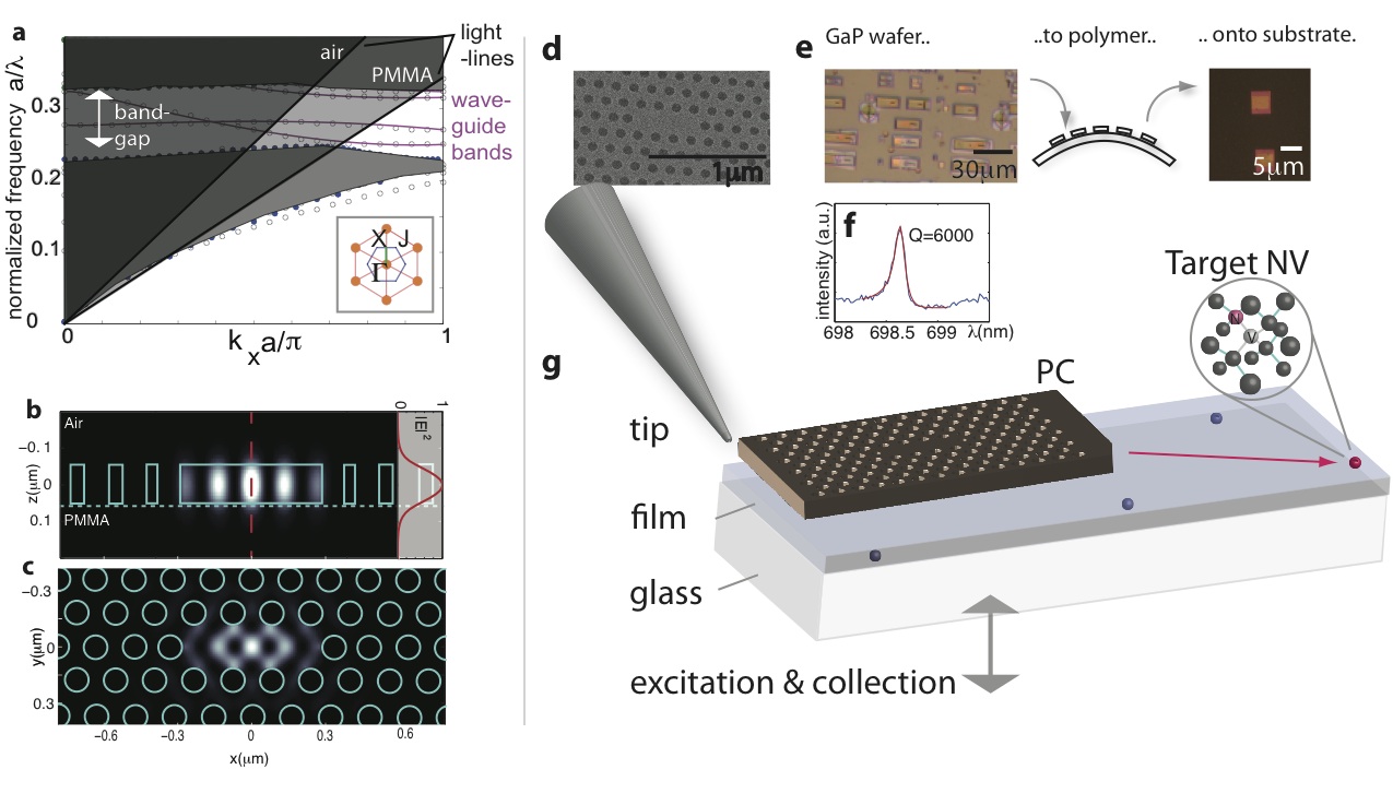
We demonstrate a technique for deterministic positioning of micron-scale PC slabs that support high quality factor () cavity modes with nanometer-scale features. When such a cavity is scanned over the sample, it can be used for deterministically coupling to optically active systems with sub-wavelength resolution via the evanescent field. By appropriate design of PC cavities and waveguides, these systems combine sub-wavelength resolution, high throughput, and cavity-enhanced sensitivity. In particular, they can be deterministically interfaced with isolated optical emitters.
In our experiments, the PC consists of a triangular lattice of air holes in a gallium phosphide (GaP) membrane, creating an optical bandgap that confines light in the slab to a cavity region. The bandgap along the crystal direction is shown in the dispersion diagram in Figure 1(a). Confinement in the vertical direction occurs through total internal reflection (TIR) for modes with frequencies below the air light-line indicated in Figure 1(a). A row of missing holes supports band modes which form bound cavity states when terminated on two sides. We employ a three-hole defect cavity Noda2003Nature whose geometry is optimized for use on a Poly(methyl methacrylate) (PMMA) substrate with a refractive index of . The TIR-confined region in k-space is smaller on top of the PMMA, as sketched in Figure 1(a), but simulations indicate that the value can still be above . The cavity has a mode volume , where is the refractive index of GaP at nm. The fundamental mode of the PC cavity is depicted by its energy density in Figure 1(c). The cross section in Figure 1(b) shows the evanescent tail of the mode that couples to emitters.
We fabricate GaP PC nanocavities by a combination of electron beam lithography and dry etching 2008.APL.Rivoire-Vuckovic.GaP_PC of a 108 nm membrane of GaP on top of a 940 nm-thick sacrificial layer of a Al0.85Ga0.15P. A wet etch removes the sacrificial layer, leaving free-standing photonic crystal membranes. The scanning electron micrograph (SEM) of a resulting PC nanocavity is shown in Figure 1(d). Reflectivity measurements of freestanding cavities indicate that quality factors (Q) of these cavities can exceed , the maximum value that can be measured with the resolution of our spectrometer (Figure 1(f)). However, in the remainder of this paper we will study cavities with typical values below 1000, since these were more reliably fabricated in large numbers, permitting systematic studies. To transfer cavities, we press the GaP chip against a flexible polymer layer of Polydimethylsiloxane (PDMS), which separates the PC membranes from the chip while preserving their arrangement. The adhesion between the membranes and the PDMS is weak enough so that the GaP structures can be stamped onto the sample that is to be imaged, as shown in Figure 1(e). In our demonstration, the sample consists of nm diamond nanocrystals that are dispersed on a glass slide covered by a nm thick layer of PMMA, for which the transfer process succeeds with probability for each membrane. The sample is mounted in a scanning confocal microscope with an oil immersion lens. A tungsten tip with radius m is used to scan and position a PC nanocavity with nanometer resolution (Figure 1(g)).
.
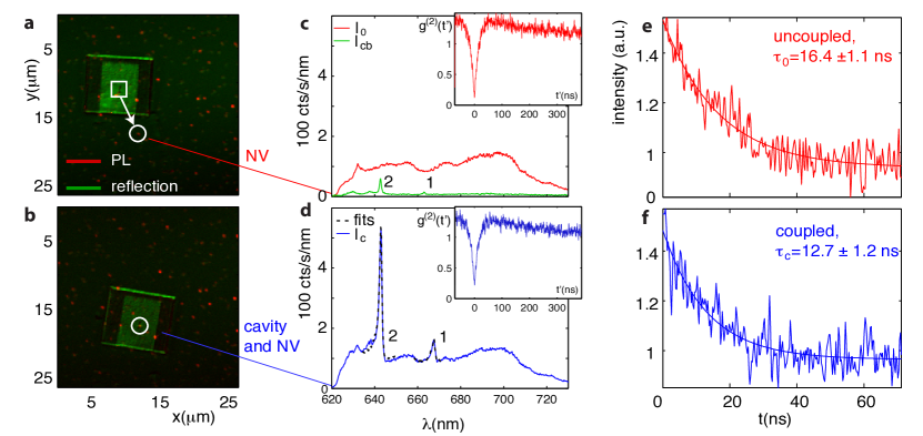
Figure 2(a) shows a room-temperature photoluminescence (PL) image of a typical sample (red signal) obtained by scanning a green excitation laser across the surface with galvanometric mirrors. The PL spots in the image correspond to single or clusters of NV centers in diamond nanocrystals. The PC nanocavity can be located with the excitation laser reflection (green in Figure 2(a)) as well as weak fluorescence originating from impurities in GaP and PMMA (green curve in Figure 2(c)). The PC fluorescence clearly shows two resonances at nm and with quality factors and . These quality factors are rather low because of variabilities in the fabrication; we saw no degradation due to the transfer onto the PMMA substrate. By collecting spectra at different points within the cavity, we can identify peak as the fundamental mode depicted in Figure 1(c) and peak as two nearly degenerate, oppositely polarized higher-order modes of the cavity. The technique and results of the spatially resolved cavity spectrum are discussed in Appendix C.
We achieve deterministic coupling between the NV and the nanocavity by first selecting a ‘target’ NV (indicated in Figure 2(a)). This center exhibits a broad spectrum (Figure 2(c)), which is characteristic of NV centers and results from a broad phonon sideband extending from 640 to 800 nm. Importantly, the emission exhibits a strongly anti-bunched autocorrelation (inset), indicating that it results from a single emitter. To couple this emitter to the cavity, we position the PC membrane over the target NV using the tungsten tip. As shown in Figure 2(d), the PL spectrum changes dramatically and shows strong peaks on resonance with the cavity modes. The intensities of these peaks are far higher than the cavity background, . Moreover, the autocorrelation of the coupled NV-cavity system is again strongly anti-bunched (Figure 2(d)), indicating that it is driven by emission of the NV center. We also verified the electronic triplet state of the coupled NV by electron spin resonance measurements, as shown in Appendix E.
The SE rate of an NV center is also modified by the presence of the PC slab. Specifically, Figures 2(e) and (f) show that the lifetimes of the uncoupled and coupled NV centers are ns, respectively. The PL spectra on and off the PC coupled with lifetime measurements allow the determination of the spectrally resolved SE rate enhancement, , of the coupled emitter via the relation (see Appendix A): the analysis of the data in Figure 2 yields and (the full curve is plotted in the Appendix).
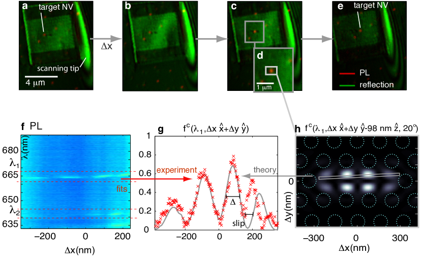
We next demonstrate the spatial resolution of our method. By monitoring the fluorescence spectrum while scanning the cavity over the NV, we can map out the near-field emitter-cavity coupling. This is demonstrated in Fig 3(a-e), where we scan the cavity along its longitudinal (x-axis) over the sample in 3.4 nm steps. Figure 3(f) presents a series of PL spectra acquired as the cavity moves over the emitter, and reveals an intensity oscillation with a period corresponding to one PC lattice spacing, nm. This oscillation corresponds to the spatially dependent SE modification, which is directly proportional to the cavity’s electric field intensity.
To analyze our observations, we note that the fluorescence of the coupled NV-cavity system is given by the emission directly from the NV, the emission through the cavity, and interference between the two:
| (1) |
where , , and determine the relative contributions of the NV, the cavity, and their interference, respectively, which depend on the collection geometry and coupling to the collection fiber. This relation is derived in Appendix F. gives the Lorentzian line shape of the cavity resonance at with linewidth , and accounts for the phase difference at the collection point between the direct NV emission and the emission through the cavity. The factor is the SE rate enhancement of transitions in the phonon sideband of the NV with respect to the background emission rate into non-cavity modes.
The coefficients , , and can be estimated from our experimental data as follows. Because of the high numerical aperture of our objective, nearly half of the emission from the cavity and the NV is collected: this observation suggests . When the signal is collected through a single-mode fiber, the interference term represented by becomes important and results in Fano-like features in the spectrum (see Appendix D) 2009.OpEx.Barclay-Santori-Painter . However, we find that the interference term vanishes when a multi-mode fiber is used, and we can set . A fit of Eq.1 to the spectrum in Figure 2(d) then yields .
Since the signal in Figure 3(f) is proportional to , we can now use Eq.1 to compare the measured cavity signal to theory. Figure 3(g) plots the fitted values of for the fundamental cavity mode frequency , as shown in the red crosses. By comparing the experimental values to predictions for the cavity mode, we find a match between experiment and theory for an NV dipole that is nm from the PC surface, as expected from the PMMA thickness, and at an angle of to the -axis, obtained from the best fit to the data. For these conditions, the predicted value of SE rate modification corresponds to the track graphed in Figure 3(h), in good agreement with experimental observations. A small discrepancy in the fit at nm results primarily from positional slip of the PC cavity that can build up during the scan, a problem which could be improved by rigidly attaching the membrane to a stiffer scanning tip.
The high spatial resolution and frequency-selective modification of spontaneous emission opens new possibilities for efficient interfacing of promising solid state qubits via optical fields. For instance, while the NV center is a promising system for quantum information processing, only the emission occurring into the zero phonon line (ZPL) is suitable for coherent optical manipulation. The frequency-selective emission enhancement demonstrated here potentially allows us to direct most of the emission of the selected NV centers into the ZPL. Furthermore, the hybrid approach is compatible with narrow linewidth NV emitters in bulk diamond at low temperature. This opens the door for applications ranging from quantum repeaters to single photon nonlinear optics. Moreover, although we have focused here on NV centers, our scanning technique provides a ‘cavity QED interface’ that can be of use to a broad range of solid state qubits.
Furthermore, the PC scanning technique can serve as a new imaging approach with sub-wavelength resolution and high throughput, which we term a Scanning Cavity Microscope (SCM). Unlike other near-field probes that compromise the signal intensity to achieve high spatial resolution, SCM enables large count rates: in the demonstration shown here, we record up to photons/s from a single NV, exceeding collection rates reported to date with far field optics. This can be further improved by efficiently out-coupling through cavity-coupled waveguides. In addition, the spatial resolution of the SCM is determined by the feature size of the confined field, which is nm for this cavity. This in-plane resolution may be improved substantially using cavity modes with small feature sizes, as in slot-waveguide cavities 2005.PRL.Robinson-Lipson.slot-cav . These qualities make the SCM a promising tool for label-free single molecule studies 2007.Science.Armani-Vahala.sensing ; 2002.JPCB.Moerner.single-molecle-spectroscopy or high-resolution studies of local index variations in thin films 1979.ApplOpt.Pulker.optical_thin_films ; 2009.RevSciInstr.Bernal.SNOM_refr_index . We note that a scan acquired by moving the photonic crystal membrane across the surface may need to be de-convolved by the response function of the cavity mode, as described in Appendix G. Beyond high resolution and throughput, the SCM adds the capability to modify the spontaneous emission rate to near-field microscopy. This opens new possibilities for direct investigations of decay channels of optical emitters, such as light emitting diodes or fluorophores; for instance, by monitoring the emission intensity while effecting a known change in the radiative emission rate, the relative nonradiative recombation rate may be inferred, allowing a direct estimate of the radiative quantum efficiency of the material.
Appendix A Wavelength-resolved excited state recombination rates
The excited state of the isolated NV- decays through a set of radiative channels which we distinguish by their wavelength and describe by the recombination rate , and nonradiative recombination described by a term . We consider the NV at some position from the cavity, and assume that it is pumped into the excited state at some rate . Then the emission spectrum at wavelength is given by
| (2) | |||||
| (3) |
where is the collection efficiency, is the excited state decay rate, and is a proportionality constant. The term can be identified as the fraction of the total recombination rate that occurs through wavelength . The decay rate can be obtained from a lifetime measurement, . The ratio of the spectra at position and the ‘bulk position’ (away from the PC slab) gives:
| (4) |
If the pump rate and collection efficiency are equal, we have
| (5) | |||||
| (6) |
where the Purcell factor . For a position where the NV and cavity are aligned on top of each other, is plotted in Figure 5.

Appendix B Photon correlation measurements
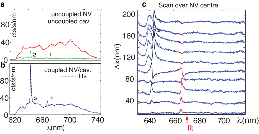
The photon correlation measurement is performed with a Hanbury Brown / Twiss (HBT) setup. The PL is directed to a beam splitter, after which the two arms are coupled through single mode fibers (SMF) to single photon detector modules (Perkin Elmer). A time-correlated counting module is used to assemble the histogram of clicks on the two detectors. Figure 4 shows the spectra collected through the SMF for the coupled and uncoupled positions of the cavity.
Appendix C Characterization of cavity modes
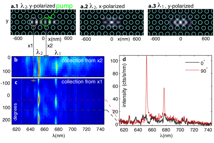
To further characterize the cavity resonances experimentally, we measured the polarization dependence of the emission collected from two different locations while pumping the NV near the center of the cavity. These positions are indicated as and in Figure 6(a), together with the simulated electric field energy density for three relevant cavity modes. Collecting from the pump location , we observe the mode at 667 nm to be strongly polarized, while the mode at 643 nm exhibits only weak polarization dependence (Figure 6(b)), for a total of three modes. From , we only observe polarized modes at and . From these observations, we conclude that the peak at corresponds to the two modes shown in Figure 6(a.1,a.2) with nearly degenerate frequency (within the relatively broad linewidth), opposite polarization, and different spatial extent. The peak at indeed corresponds to a single mode, which we identify as the lowest-frequency confined state of the L3 cavity.
Appendix D Single mode fiber spectra
When the multi-mode fiber was replaced with a single mode fiber, the spectra in Fig. 2(c,d) in the main text show the same pattern, but at a reduced count rate, as displayed in Figure 4.
The simultaneous collection from the cavity and the emitter results in interference at the detector. As the cavity is scanned over the NV emitter, we observe Fano-like features at the cavity resonances shown in Figure 4(b), which are fit well by Eq.1 with . Such interface effects have been described before in microdisks2009.OpEx.Barclay-Santori-Painter and microspheres2008.NanoLett.Benson.microdisk_diamond_coupling coupled to single NV emitters. In microscopy, the intereference signature may be used to better distinguish a single emitter from the background.
Appendix E Electron Spin Resonance and Rabi Oscillations
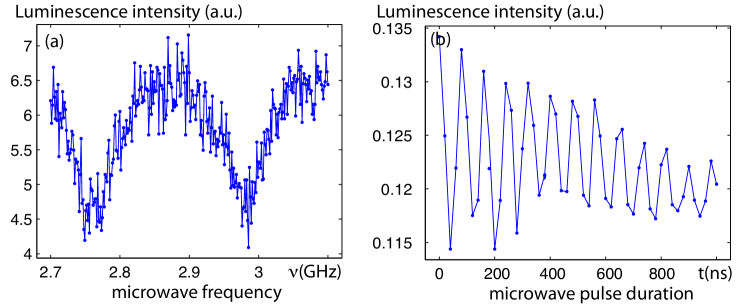
The NV center has two unpaired electrons in a triplet configuration with a zero-field splitting of GHz between and sublevels. The excited state decay rates allow spin-sensitive detection since the fluorescence is reduced for the states 2006.PRB.Manson.NV_model . In the spin measurements described here, the sublevels were additionally split by an external magnetic field produced by a permanent magnet. Figure 7(a) shows the microwave transitions from to , which are evident in the intensity of the cavity-coupled NV as a function of a microwave field of intensity , while Figure 7(b) shows driven spin oscillations when the NV spin is optically initialized in , excited with a microwave pulse for a duration at a frequency GHz, and optically detected using a pulse sequence described in elsewhere 2006.Science.Childress.coherent_nuclear_spin_dynamics .
Appendix F Spontaneous emission modification
The Hamiltonian describing a NV (lowering operator ) coupled to a cavity mode (with annihilation operator , without considering environment interactions, is given by
| (7) |
where is NV-cavity detuning and the reference energy is the mean of NV and cavity energy.
The Master equation is given by
| (8) |
where , and account for NV population decay, cavity population decay and NV pure dephasing; and .
We consider the subspace of 0 or 1 excitation in the NV , and 0 or 1 excitations in the cavity From Eq. 8 we obtain the Maxwell Bloch equations2009.PRA.Poizat.dephasing
| (9) | |||
| (10) |
These two coupled equations are solved with the initial condition ; in the subspace considered here. We define and and , . The time-dependent solution is
| (12) |
and
| (13) |
The electric field emitted by the NV and cavity is described by
| (14) |
where and describe the spatial profiles of the emission from the NV center and the cavity. The emission is collected through a lens into an optical fiber (either single mode or multi-mode) with a set of orthonormal modes {}. The field at the output of the fiber, which is directed at the detector, is given by
| (15) |
where . The spectrum is obtained from the Quantum Regression theorem, . We make the assumption that the linewidth of the NV center is much broader than the NV-cavity detuning and all other loss or coupling rates: . After normalizing the spectrum by the bare NV emission spectrum, we obtain
| (16) | |||||
where denotes the Purcell factor at position and orientation of the NV in the field of the cavity. In this experiment, it is not possible to calculate the term directly because of uncertainty in the coupling of the NV and cavity modes to the fiber. In general, we therefore represent the detected spectrum as
where the real coefficients are obtained by fits to the data. We obtain good fits for the single mode fiber with , and for the multi-mode fiber with .
Appendix G Imaging of general samples
The signal in Fig. 3 in the main text represents the convolution of the emitter’s spatial profile, , and the spectrometer signal given in Eq.1. Thus, , where is the displacement along the path of . Since the NV center is less than 1 nm in size, we consider it as a delta function, so that , giving the response function of our scanning probe. Once this response function is known, the SCN maps a general sample by first measuring the convolved image and then deconvolving by the known response to obtain .
References
- (1) C. J. Hood, T. W. Lynn, A. C. Doherty, A. S. Parkins, and H. J. Kimble. The Atom-Cavity Microscope: Single Atoms Bound in Orbit by Single Photons. Science, 287(5457):1447–1453, 2000.
- (2) Andrea M. Armani, Rajan P. Kulkarni, Scott E. Fraser, Richard C. Flagan, and Kerry J. Vahala. Label-Free, Single-Molecule Detection with Optical Microcavities. Science, 317(5839):783–787, 2007.
- (3) D. Englund, A. Faraon, I. Fushman, N. Stoltz, P. Petroff, and J. Vučković. Controlling cavity reflectivity with a single quantum dot. Nature, 450(6):857–61, 2007.
- (4) K. Srinivasan and O. Painter. Linear and nonlinear optical spectroscopy of a strongly coupled microdisk-quantum dot system. Nature, 450:862–865, December 2007.
- (5) Masayuki Fujita, Shigeki Takahashi, Yoshinori Tanaka, Takashi Asano, and Susumu Noda. Simultaneous Inhibition and Redistribution of Spontaneous Light Emission in Photonic Crystals. Science, 308(5726):1296–1298, 2005.
- (6) D. Englund, D. Fattal, E. Waks, G. Solomon, B. Zhang, T. Nakaoka, Y. Arakawa, Y. Yamamoto, and J. Vuckovic. Controlling the Spontaneous Emission Rate of Single Quantum Dots in a Two-Dimensional Photonic Crystal. Phys. Rev. Lett., 95:013904, July 2005.
- (7) Stefan Strauf, Nick G. Stoltz, Matthew T. Rakher, Larry A. Coldren, Pierre M. Petroff, and Dirk Bouwmeester. High-frequency single-photon source with polarization control. Nat Photon, 1(12):704–708, December 2007.
- (8) J. I. Cirac, P. Zoller, H. J. Kimble, and H. Mabuchi. Quantum State Transfer and Entanglement Distribution among Distant Nodes in a Quantum Network. Phys. Rev. Lett., 78(16):3221–24, April 1997.
- (9) H.-J. Briegel, W. Dür, J. I. Cirac, and P. Zoller. Quantum repeaters: The role of imperfect local operations in quantum communication. Phys. Rev. Lett., 81(26):5932–5935, Dec 1998.
- (10) T. Yoshie, A. Scherer, J. Hendrickson, G. Khitrova, H. M. Gibbs, G. Rupper, C. Ell, O. B. Shchekin, and D. G. Deppe. Vacuum Rabi splitting with a single quantum dot in a photonic crystal nanocavity. Nature, 432:200–203, November 2004.
- (11) K. Hennessy, A. Badolato, M. Winger, D. Gerace, M. Atature, S. Gulde, S. Falt, E. L. Hu, and A. Imamoglu. Quantum nature of a strongly coupled single quantum dot-cavity system. Nature, 445:896–899, 2007.
- (12) Michael Barth, Nils Nüsse, Bernd Löchel, and Oliver Benson. Controlled coupling of a single-diamond nanocrystal to a photonic crystal cavity. Opt. Lett., 34(7):1108–1110, 2009.
- (13) Paul E. Barclay, Kai-Mei Fu, Charles Santori, and Raymond G. Beausoleil. Hybrid photonic crystal cavity and waveguide for coupling to diamond nv-centers. Opt. Express, 17(12):9588–9601, 2009.
- (14) Igal Bayn and Joseph Salzman. Ultra high-q photonic crystal nanocavity design: The effect of a low- slab material. Opt. Express, 16(7):4972–4980, 2008.
- (15) Christine Kreuzer, Janine Riedrich-Möller, Elke Neu, and Christoph Becher. Design of photonic crystal microcavities in diamond films. Opt. Express, 16(3):1632–1644, 2008.
- (16) P. Neumann, N. Mizuochi, F. Rempp, P. Hemmer, H. Watanabe, S. Yamasaki, V. Jacques, T. Gaebel, F. Jelezko, and J. Wrachtrup. Multipartite Entanglement Among Single Spins in Diamond. Science, 320(5881):1326–1329, 2008.
- (17) L. Jiang, J. S. Hodges, J. R. Maze, P. Maurer, J. M. Taylor, D. G. Cory, P. R. Hemmer, R. L. Walsworth, A. Yacoby, A. S. Zibrov, and M. D. Lukin. Repetitive Readout of a Single Electronic Spin via Quantum Logic with Nuclear Spin Ancillae. Science, 326(5950):267–272, 2009.
- (18) G. D. Fuchs, V. V. Dobrovitski, D. M. Toyli, F. J. Heremans, and D. D. Awschalom. Gigahertz Dynamics of a Strongly Driven Single Quantum Spin. Science, page science.1181193, 2009.
- (19) Y. Akahane, T. Asano, B.-S. Song, and S. Noda. High-Q photonic nanocavity in a two-dimensional photonic crystal. Nature, 425:944–947, October 2003.
- (20) Kelley Rivoire, Andrei Faraon, and Jelena Vuckovic. Gallium phosphide photonic crystal nanocavities in the visible. Applied Physics Letters, 93(6):063103, 2008.
- (21) A. P. Nizovtsev, S. Ya. Kilin, C. Tietz, F. Jelezko, and J. Wrachtrup. Modeling fluorescence of single nitrogen-vacancy defect centers in diamond. Physica B: Condensed Matter, 308-310:608 – 611, 2001.
- (22) Paul E. Barclay, Charles Santori, Kai-Mei Fu, Raymond G. Beausoleil, and Oskar Painter. Coherent interference effects in a nano-assembled diamond nv center cavity-qed system. Opt. Express, 17(10):8081–8097, 2009.
- (23) Jacob T. Robinson, Christina Manolatou, Long Chen, and Michal Lipson. Ultrasmall mode volumes in dielectric optical microcavities. Phys. Rev. Lett., 95(14):143901, Sep 2005.
- (24) W. E. Moerner. A dozen years of single-molecule spectroscopy in physics, chemistry, and biophysics. The Journal of Physical Chemistry B, 106(5):910–927, 01 2002/01/12/.
- (25) H. K. Pulker. Characterization of optical thin films. Appl. Opt., 18(12):1969–1977, 1979.
- (26) Séverine Diziain, Jean-Marc Merolla, Michel Spajer, Giacomo Benvenuti, Ali Dabirian, Yury Kuzminykh, Patrik Hoffmann, and Maria-Pilar Bernal. Determination of local refractive index variations in thin films by heterodyne interferometric scanning near-field optical microscopy. Review of Scientific Instruments, 80(9):093706, 2009.
- (27) Stefan Schietinger, Tim Schröder, and Oliver Benson. One-by-one coupling of single defect centers in nanodiamonds to high-q modes of an optical microresonator. Nano Letters, 8(11):3911–3915, 09 2008/09/24/.
- (28) N. B. Manson, J. P. Harrison, and M. J. Sellars. Nitrogen-vacancy center in diamond: Model of the electronic structure and associated dynamics. Physical Review B (Condensed Matter and Materials Physics), 74(10):104303, 2006.
- (29) L. Childress, M. V. Gurudev Dutt, J. M. Taylor, A. S. Zibrov, F. Jelezko, J. Wrachtrup, P. R. Hemmer, and M. D. Lukin. Coherent Dynamics of Coupled Electron and Nuclear Spin Qubits in Diamond. Science, 314(5797):281–285, 2006.
- (30) Alexia Auffèves, Jean-Michel Gérard, and Jean-Philippe Poizat. Pure emitter dephasing: A resource for advanced solid-state single-photon sources. Physical Review A (Atomic, Molecular, and Optical Physics), 79(5):053838, 2009.