A spin quantum bit with ferromagnetic contacts for circuit QED
Abstract
We theoretically propose a scheme for a spin quantum bit based on a double quantum dot contacted to ferromagnetic elements. Interface exchange effects enable an all electric manipulation of the spin and a switchable strong coupling to a superconducting coplanar waveguide cavity. Our setup does not rely on any specific band structure and can in principle be realized with many different types of nanoconductors. This allows to envision on-chip single spin manipulation and read-out using cavity QED techniques.
pacs:
03.67.Lx,73.23.-b,32.80.-tAchieving a strong coupling between a single atom and a single photon trapped in a cavity has been instrumental for studying the interaction of light and matter at the most elementary levelQED . Recently, what was originally belonging to the realm of quantum opticsRaimond ; T. Yoshie ; J. P. Reithmaier has been brought into superconducting chips: two level superconducting circuits (artificial atoms) have been embedded into superconducting coplanar waveguide cavities, in the context of circuit Quantum ElectroDynamicsWallraff . Extending further this “transfer” to the field of nano-fabricated circuits could offer a very interesting platform for the study of entanglement and decoherence in many body systems.

The electronic spin of nanoconductors raises a strong interest in the fields of quantum information and quantum coherence, because it is generally expected to be more robust to decoherence than the orbital degrees of freedomHanson . Coupling the spin of a nanoconductor to cavity photons seems particularly attractiveChildress . Nanofabricated circuits are naturally compatible with on-chip superconducting waveguide architectures. However, two major difficulties have to be overcome. First, a strong coupling between a spin and an electric field is intrinsically difficult to achieve. Second, in architectures integrating several spins, the selective manipulation of each spin is a challenge. The electrical schemes available for local spin manipulation Tokura ; Nowack ; Trif1 and spin/photon couplingTrif2 ; Burkard rely on the use of a strong external static magnetic field, which is not naturally compatible with strong photon confinement in superconducting cavitiesFrunzio . More generally, a scheme allowing one to switch off efficiently is lacking, for nanoconductor based qubits as well as superconducting qubitsGirvin . An alternative way to spin-polarize the spectrum of a nanoconductor is to use ferromagnetic insulator () contacts, which have a very strong internal Zeeman field. The hybridization of the nanoconductor orbitals with the first atomic layers of the leads to an effective Zeeman field inside the nanoconductor itself. This effect is quite universal since it can arise in very different systems, such as carbon nanotubes Cottet2006 ; S. Sahoo ; Hauptman:08 , InAs quantum dots InAs or thin superconducting layersTedrow ; Cottet2009 . In this letter, we propose theoretically a scheme for a spin qubit based on a double quantum dot contacted to ferromagnetic insulators. Interface exchange effects enable an all electric manipulation of the spin and a switchable strong coupling to a superconducting cavity. First, our scheme is compatible with superconducting architectures since it can be realized using layer designs which minimize stray fields. Second, it is generic in the sense that it does not rely on intrinsic nanoconductor properties such as spin orbit couplingTrif2 or hyperfine interactionBurkard . Third, it is relatively robust since the contact-induced effective fields can be adjusted in numerous ways, from the fabrication to the operation of the quantum dots. This allows to envision single spin manipulation and read-out using cavity QED techniques.
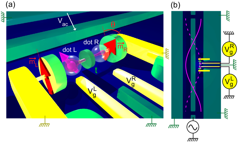
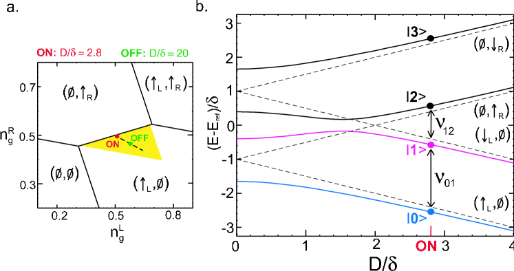
We first consider two generic quantum dots and coupled through a tunnel barrier with a hopping constant (see Fig. 1). Each dot is connected to a grounded normal metal reservoir through a layer, and capacitively coupled to a DC gate with voltage , which allows to tune the chemical potential of the dot. The double dot system is placed between the center and ground conductors of a superconducting coplanar waveguide cavity, which conveys a voltage . We take into account one orbital level for each quantum dot. The dots have strong self and mutual charging energies, so that, by tuning properly and , we reach a regime where the total number of electrons on the double dot system is constantly equal to 1 (see Fig. 2). The tunnel rates through the are sufficiently small so that cotunneling processes between the dot and the normal reservoirs can be neglected. Our key ingredient is the contact-induced effective spin splittings in dots . The effective fields in dots and are colinear to the magnetizations and of the left and right , which form an angle . For later use, we note a double dot state with the dot in state . Here, can be the empty state or a singly occupied state with a given spin (for instance and refer to spin states parallel and antiparallel to respectively). With the above assumptions, the simplified double dot hamiltonian writes
| (1) |
Here, and , with , refer to the identity and Pauli matrices in the left/right orbital subspace and the spin subspace respectively. We note the energy shift between the states and for . This quantity can be tuned with the dots’ gate voltagesEPAPS . For simplicity, we assume . We define an ”ON” working point , with , and . At the ON point, we note , with , the eigenstates of , with energies growing with the index . The two lowest eigenstates and both have an overlap to the right dot of only, and they correspond to and spin states to a good approximation since we obtain
, , and . We obtain a transition frequency accessible with current microwave technology. Importantly, the transition frequency between the states and is significantly different from . The double dot circuit is thus sufficiently anharmonic to be operated as an effective two level system , called ”spin qubit” in the following. When is changed to and , one obtains a coupling element because the direction of the overall field felt by the electron slightly changes. Importantly, when the capacitances connected to dots and are asymmetric, one has EPAPS . This property combined with allows a transverse coupling of the spin qubit to the electric field conveyed by the waveguide.

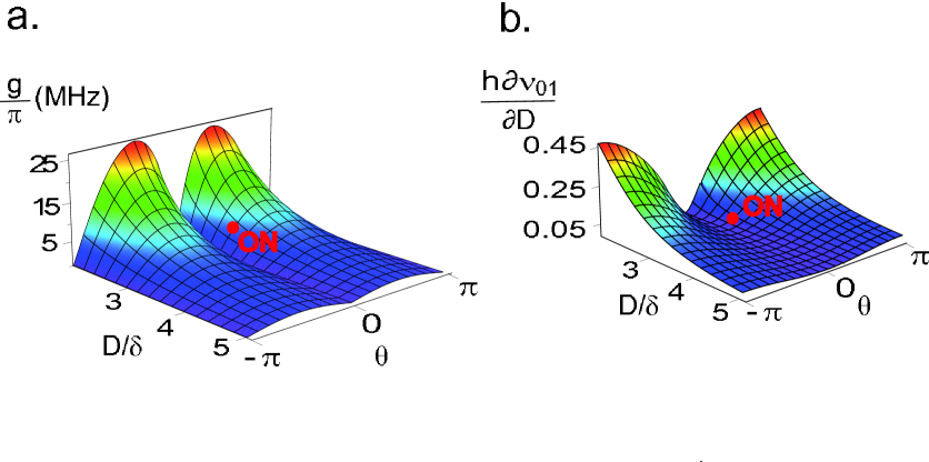
In these conditions, Rabi oscillations between the states and can be obtained by applying an oscillating voltage with frequency to the waveguide center conductor. Using the rotating wave approximation and the quantization rule Blais , with the annihilation and creation operators for photons of the waveguide cavity, the set of the spin qubit and cavity can be described with a standard Jaynes-Cummings hamiltonian with , and , , the Pauli operators in the subspace . Using realistic values for the circuit capacitancesEPAPS and , we obtain a strong spin/electric field coupling at the ON point, i.e. in terms of vacuum Rabi frequency, a value comparable to that obtained in Ref. Wallraff, . With such a coupling, the readout of the qubit state can be performed by measuring the dispersive shift of the cavity resonance frequencyBlais . Besides, a distant coupling between two qubits can be realized by exchange of virtual cavity photonsMajer . Importantly, our setup allows us to strongly decrease the spin/cavity coupling by increasing . For instance, we obtain at the OFF point where Outside the qubit manipulation stage, the qubit can be placed at the OFF point to minimize decoherence due to the coupling to the cavityHouck . This also allows us to switch off very efficiently the coupling between two qubits via virtual cavity photons, with almost no change of the qubit transition frequency. Then, the qubit has to be placed at the ON point for the manipulation of its quantum state. This can be performed by using appropriate gate voltage pulses. Note that also depends on the angle as shown in Fig. 3.a. However, using a constant imposed e.g. by the shape of the layers should be sufficient in practice.
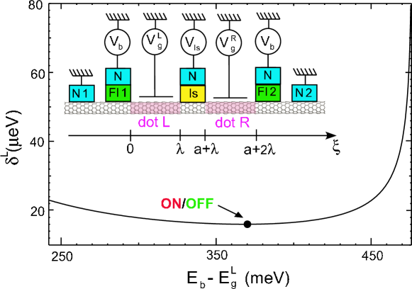
Reaching the strong coupling regime requires that the coherence times of the spin and the cavity photons are longer than . Since our setup does not use any external magnetic field, it is compatible with using a superconducting cavity with a good quality factor. Nevertheless, the coherence time of the spin qubit can be limited by various mechanisms causing dephasing and relaxation. These mechanisms depend on the structural properties of the nanoconductors used. In principle, our scheme can be implemented with various types of nanoconductors, such as e.g. silicon nanowiresShaji ; Jonker or SWNTs. So far, the latter are the most advanced nanoconductors for realizing our setup. Semiconducting SWNTs are particularly suitable for defining double quantum dots, using top gates which allow one to tune the interdot coupling Mason . Contact-induced Zeeman effective fields have already been observed in SWNTsS. Sahoo ; Hauptman:08 . Besides, multi-dot systems with ferromagnetic leads and a local gate control have already been realized in the open regimeCPF . We consider a SWNT above which several gates and contacts are evaporated (inset of Fig. 4). The central electrostatic gate enclosing an insulating layer is used to define . The two dots are delimited by and two other gates which enclose ferromagnetic insulating layers and . Here, the role the layers of our generic setup is played by the SWNT sections below and . Following the approach of Ref. Dani, , these SWNT sections are subject to an effective Zeeman field . The electron confined in dot feels through its evanescent tail, which leads to . We describe the electronic bands of the SWNT with the Dirac-like hamiltonian
| (2) |
Here, and with are the Pauli matrices on the A/B atoms and valley subspaces, is the radius of the SWNT and is the SWNT Fermi velocity. The term describes a coupling between the and bands, responsible for an orbital level splitting currently observed in experimentsLiang ; Sapmaz . We note and the longitudinal and azimuthal SWNT coordinates. To obtain the spectral properties of dots and separately (), we use , and for dot , and , , and for dot . These potential profiles can be adjusted with the various electrostatic gates shown in Fig. 4. Remarkably, we find that depends on , but also on the size and the active orbitals of dots . Therefore, our scheme can work for a wide range of because can be easily adjusted to the value required in the generic model. Here, we use , consistently with Ref. Dani, , and . We define the states and [ and ] as the lowest pair of spin-dependent levels in the conduction band of dot . Remarkably, for , with the SWNT bandgap, we obtain a sweet spot , with . One has at the ON/OFF points, thus . Finally, the interdot coupling can be calculated from the overlap between the dots’ orbitals. The value can be obtained by varying and , without affecting significantly the sweet spot (not shown).


The spin coherence time is expected to be comparably long in SWNTS. Current estimates based on the spin-orbit interaction in 13C-free SWNTs lead to millisecondsBulaev . Since our setup provides a new way to control the spin degree of freedom, it is a priori subject to specific decoherence mechanisms which we evaluate below. First, low frequency charge noise picked up by the dot gates risks to induce fluctuations of and thus , which will limit the spin dephasing time . Since decreases with , the choice of results from a compromise between having a low and a large . This compromise also requires to use a relatively small value for , although is maximal for values of close to (see Fig. 3.b). Using a semiclassical approach, we estimate and at the ON and OFF points, using the charge noise amplitude measured in non-suspended SWNTsHerrmann . Second, from Eq. (1), corresponds to . Hence, charge noise can also dephase the qubit through fluctuations of . However, it is possible to minimize this effect by working at the sweet spot in both the ON and OFF states (see Fig. 4). This gives a dephasing time . Third, the electron/phonon interaction conserves spin. However, since the states and have slight components in and respectively, they can relax due to electron/phonon interaction. To evaluate this effect, we take into account the acoustic mode most strongly coupled to electrons, i.e. the stretching modeAndo . We assume that the phonons in dots and are confined and decoupled due to the massive top gates. We obtain and at the ON and OFF point respectivelyEPAPS . Quite generally, using suspended nanoconductors could reduce further decoherence, by decreasing the charge noise picked up by the device, and also by reducing the phonon-induced thanks to a phononic Purcell-like effect. For instance, we estimate and in the SWNT setup, for phonons confined inside dots and with a quality factor . In principle, one can also expect relaxation due to the coupling to the cavity, similar to what observed with superconducting qubitsHouck . However, at the OFF point, we expect the cavity to be a marginal source of decoherence since is almost switched off. At the ON point, it is in principle possible to reduce the cavity-induced relaxation by improving the cavity designWang . Hence, we have focused on decoherence sources more specific to our qubit design. In summary, for a non-suspended SWNT setup, we finally obtain a promising total decoherence time at the ON point. Remarkably, at the OFF point, we obtain while is reduced by a factor of compared to the ON point. This suggests that our spin qubit could also be used as a quantum register.
Acknowledgements.
We gratefully acknowledge fruitfull discussions with J. M. Raimond, B. Douçot and H. Jaffrès. This work was financed by the CNano Ile de France contract SPINMOL.References
- (1) H. Mabuchi and A. Doherty, Science 298, 1372 (2002).
- (2) J.M. Raimond, M. Brune and S. Haroche Rev. Mod. Phys. 73, 565 (2001).
- (3) T. Yoshie et al. Nature 432, 200 (2004).
- (4) J.P. Reithmaier et al. Nature 432, 197 (2004).
- (5) A. Wallraff et al. Nature 431, 162 (2004).
- (6) R. Hanson et al., Rev. Mod. Phys. 79, 1217 (2007).
- (7) L. Childress, A.S. Sørensen, A. S. and M. D. Lukin, Phys. Rev. A 69, 042302 (2004).
- (8) Y. Tokura et al., Phys. Rev. Lett. 96, 047202 (2006).
- (9) K. C. Nowack et al. Science 318, 1430 (2007).
- (10) M. Trif et al., Phys. Rev. Lett. 101, 217201 (2008).
- (11) M. Trif, V. N. Golovach and D. Loss, Phys. Rev. B 77, 045434 (2008).
- (12) G. Burkard and A. Imamoglu, Phys. Rev. B 74, 041307(R) (2006).
- (13) L. Frunzio et al. IEEE Trans. Appl. Supercond. 15, 860 (2005).
- (14) S. M. Girvin, M. H. Devoret, R. J. Schoelkopf, Phys. Scr. T 137, 014012 (2009).
- (15) A. Cottet and M.-S. Choi, Phys. Rev. B 74, 235316 (2006).
- (16) S. Sahoo et al. Nature Phys. 1, 99 (2005).
- (17) J.R. Hauptmann, J. Paaske, and P. E. Lindelof, Nature Phys. 4, 373 (2008).
- (18) C. Feuillet-Palma et al., Phys. Rev. B 81, 115414 (2010).
- (19) K. Hamaya et al. Appl. Phys. Lett. 91, 022107 (2007).
- (20) P. M. Tedrow, J. E. Tkaczyk and A. Kumar, Phys. Rev. Lett. 56, 1746 (1986).
- (21) A. Cottet et al., Phys. Rev. B 80, 184511 (2009).
- (22) See EPAPS
- (23) A. Blais et al. Phys. Rev. A 69, 062320 (2004).
- (24) J. Majer et al. Nature 449, 443 (2007).
- (25) N. Shaji et al., Nature Phys. 4, 540 (2008).
- (26) B.T. Jonker et al., Nature Phys. 3, 542 (2007).
- (27) N. Mason, N., M.J. Biercuk, and C.M. Marcus, Science 303, 655 (2004).
- (28) H. Haugen, D. Huertas-Hernando and A. Brataas, Phys. Rev. B 77, 115406 (2008).
- (29) D. V. Bulaev, B. Trauzettel and D. Loss, Phys. Rev. B 77, 235301 (2008).
- (30) L.G. Herrmann et al. Phys. Rev. Lett. 99, 156804 (2007).
- (31) H. Suzuura and T. Ando, Phys. Rev. B 65, 235412 (2002).
- (32) W. Liang,M. Bockrath, and H. Park, Phys. Rev. Lett. 88, 126801 (2002).
- (33) S. Sapmaz et al., Phys. Rev. B 71, 153402 (2005).
- (34) A. A. Houck et al., Phys. Rev. Lett. 101, 080502 (2008).
- (35) H. Wang et al. arXiv:0909.0547