Heterointerface effects on the charging energy of shallow D- ground state in silicon: the role of dielectric mismatch
Abstract
Donor states in Si nanodevices can be strongly modified by nearby insulating barriers and metallic gates. We report here experimental results indicating a strong reduction in the charging energy of isolated As dopants in Si FinFETs, relative to the bulk value. By studying the problem of two electrons bound to a shallow donor within the effective mass approach, we find that the measured small charging energy may be due to a combined effect of the insulator screening and the proximity of metallic gates.
pacs:
03.67.Lx, 85.30.-z, 73.20.Hb, 85.35.Gv, 71.55.CnI Introduction
For over a decade dopants in Si have constituted the key elements in proposals for the implementation of a solid state quantum computer. Kane (1998); Vrijen et al. (2000); Skinner et al. (2003); Barrett and Milburn (2003); Hollenberg et al. (2004) Spin or charge qubits operate through controlled manipulation (by applied electric and magnetic fields) of the donor electron bound states. A shallow donor, as P or As in Si, can bind one electron in the neutral state, denoted by , or two electrons in the negatively charged state, denoted by . Proposed one and two-qubit gates involve manipulating individual electrons or electron pairs bound to donors or drawn away towards the interface of Si with a barrier material. Kane (1998); Skinner et al. (2003); Calderón et al. (2006) In general, neutral and ionized donor states play a role in different stages of the prescribed sequence of operations.
In the proposed quantum computing schemes, donors are located very close to interfaces with insulators, separating the Si layer from the control metallic gates. This proximity is required in order to perform the manipulation via electric fields of the donor spin and charge states. The presence of boundaries close to donors modifies the binding potential experienced by the electrons in a semiconductor. This is a well-known effect in Si MOSFETs, MacMillen and Landman (1984); Calderón et al. (2007) where the binding energy of electrons is reduced with respect to the bulk value for distances between the donor and the interface smaller than the typical Bohr radius of the bound electron wave-function. On the other hand, in free-standing Si nanowires with diameters below nm, the binding energy of donor electrons significantly increases Delerue and Lannoo (2004); Diarra et al. (2007) leading to a strongly reduced doping efficiency in the nanowires. Björk et al. (2009)
The continuous size reduction of transistors along years, with current characteristic channel lengths of tens of nanometers, implies that the disorder in the distribution of dopants can now determine the performance, in particular the transport properties of the devices. Voyles et al. (2002); Shinada et al. (2005); Pierre et al. (2009) In specific geometries, like the nonplanar field effect transistors denoted by FinFETs, Sellier et al. (2006) isolated donors can be identified and its charge states (neutral , and negatively charged ) studied by transport spectroscopy.
The existence of donor states in semiconductors, analogous to the hydrogen negative ion , was suggested in the fifties Lampert (1958) and is now well established experimentally. Negatively charged donors in bulk Si were first detected by photoconductivity measurements. Taniguchi and Narita (1976) The binding energies of donors, defined as the energy required to remove one electron from the ion ( free-electron) , are found experimentally to be small ( meV for P and meV for As) compared to the binding energies of the first electron (45 meV for P and 54 meV for As). For zero applied magnetic fields, no excited bound states of in bulk semiconductors Larsen and McCann (1992) or superlattices Shi et al. (1995) are found, similar to which has only one bound state in three-dimensions as shown in Refs. Pekeris, 1962; Hill, 1977.
A relevant characteristic of negatively charged donors is their charging energy, , which gives the energy required to add a second electron to a neutral donor. This extra energy is due to the Coulomb repulsion between the two bound electrons, and does not contribute in one electron systems, as . The measured values in bulk Si are meV for As and meV for P.
From the stability diagrams obtained from transport spectroscopy measurements we observe that the charging energy of As dopants in nanoscale Si devices (FinFETs) is strongly reduced compared to the well known bulk value. By using a variational approach within the single-valley effective mass approximation, we find that this decrease of the charging energy may be attributed to modifications on the bare insulator screening by the presence of a nearby metallic layer. For the same reason, we also find theoretically that it may be possible to have a bound excited state.
This paper is organized as follows. In Sec. II, we introduce the formalism for a donor in the bulk in analogy with the hydrogen atom problem. In Sec. III, we study the problem of a donor close to an interface within a flat band condition. We show experimental results for the charging energy and compare them with our theoretical estimations. We also calculate the binding energy of a triplet first excited state. In Sec. IV we present discussions including: (i) assessment of the limitations in our theoretical approach, (ii) considerations about the modifications of the screening in nanoscale devices, (iii) the implications of our results in quantum device applications, and, finally, we also summarize our main conclusions.
II Donors in bulk silicon
A simple estimate for the binding energies of both and in bulk Si can be obtained using the analogy between the hydrogen atom and shallow donor states in semiconductors. The Hamiltonian for one electron in the field of a nucleus with charge and infinite mass is, in effective units of length and energy ,
| (1) |
with . The ground state is
| (2) |
with Bohr radius and energy . This corresponds to one electron in the orbital.
For negatively charged hydrogen (H-) the two electrons Hamiltonian is
| (3) |
where the last term gives the electron-electron interaction (). As an approximation to the ground state, we use a relatively simple variational two particles wave-function for the spatial part, a symmetrized combination of atomic orbitals as given in Eq. 2, since the spin part is a singlet,
| (4) |
The resulting energy is with and (binding energy ). Bethe and Salpeter (2008) Here we may interpret as the radius of the inner orbital and of the outer orbital. This approximation for the wave-function correctly gives a bound state for but it underestimates the binding energy with respect to the value Ry, obtained with variational wave-functions with a larger number of parameters, thus closer to the ’exact’ value. Bethe and Salpeter (2008)
Assuming an isotropic single-valley conduction band in bulk Si the calculation of the and energies reduces to the case of just described. Within this approximation, an estimation for can then be obtained by considering an effective rydberg with an isotropic effective mass (we use ). We choose so that the ground state energy for a neutral donor is the same as given by an anisotropic wave-function in bulk: within a single valley approximation meV and its effective Bohr radius is with nm. In this approximation, meV. In the same way, an estimation for the charging energy can be made for donors in Si: meV. Ramdas and Rodriguez (1981)
Even though the trial wave function in Eq. (4) underestimates the binding energy, we adopt it here for simplicity, in particular to allow performing in a reasonably simple way the calculations for a negatively charged donor close to an interface reported below. In the same way, we do not introduce the multivalley structure of the conduction band of Si. The approximations proposed here lead to qualitative estimates and establish general trends for the effects of an interface on a donor energy spectrum. The limitations and consequences of our approach are discussed in Sec. IV.
| E | |||
|---|---|---|---|
| E | ; | ||
| EB | = E- E | ||
| U | = E-2E |
III Donors close to an interface
III.1 and ground states
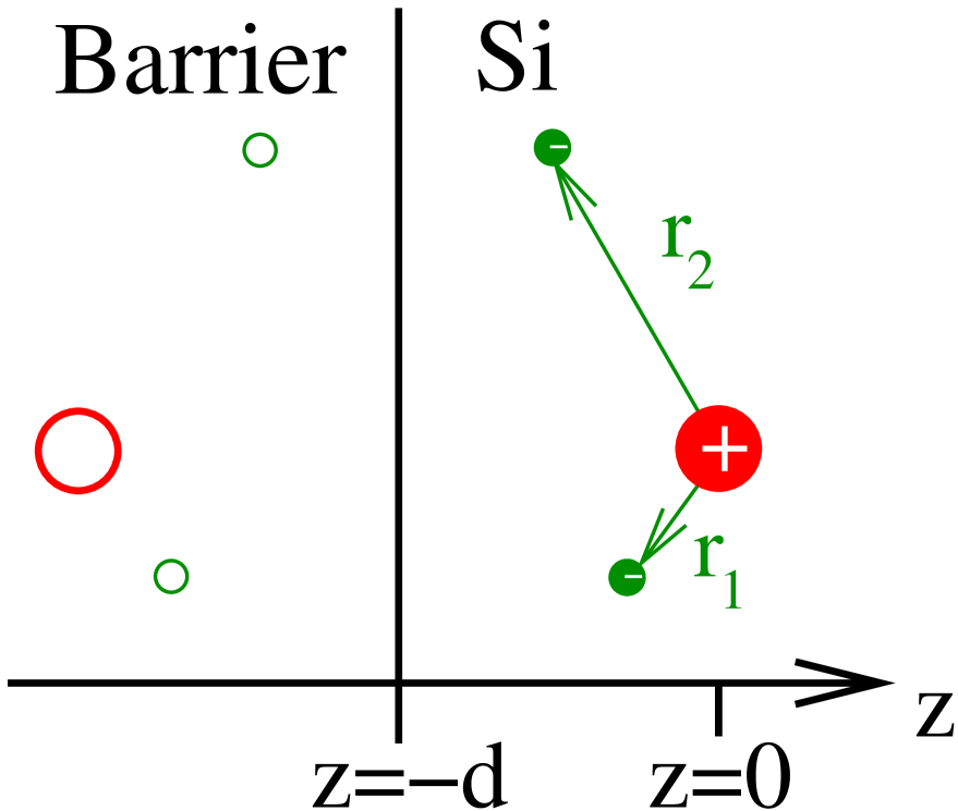
We consider now a donor (at ) close to an interface (at ) (see Fig. 1). Assuming that the interface produces an infinite barrier potential, we adopt variational wave-functions with the same form as in Eqs. (2) and (4) multiplied by linear factors () which guarantee that each orbital goes to zero at the interface. We further characterize the Si interface with a different material by including charge image terms in the Hamiltonian.
Before discussing the ionized donor , we briefly present results for the neutral donor which are involved in defining donor binding and charging energies. For this case, the Hamiltonian is
| (5) |
with as in Eq. 1 and
| (6) |
where . is the dielectric constant of the barrier material. The first term in is the interaction of the electron with its own image, and the second is the interaction of the electron with the donor’s image. If the barrier is a thick insulator, for example SiO2 with dielectric constant , ( in this case). In actual devices, the barrier is composed of a thin insulator (usually SiO2), which prevents charge leakage, plus metallic electrodes which control transport and charge in the semiconductor. This composite heterostructure may effectively behave as a barrier with an effective dielectric constant larger than Si, since , leading to an effective . Depending on the sign of , the net image potentials will be repulsive or attractive, which may strongly affect the binding energies of donors at a short distance from the interface.
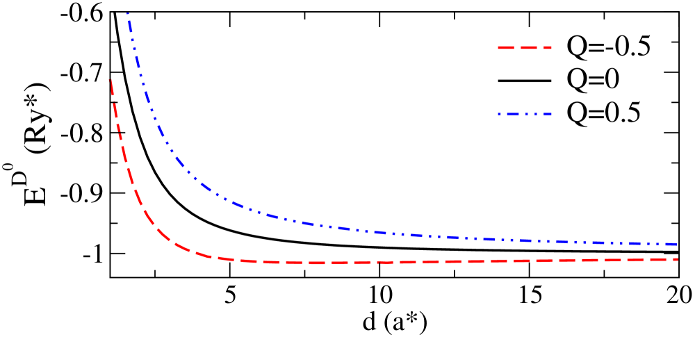
Using a trial wave-function , most of the integrals involved in the variational calculation of can be performed analytically. is shown in Fig. 2 for different values of and compare very well with the energy calculated by MacMillen and Landman MacMillen and Landman (1984) for with a much more complex trial wave-function. The main effect of the interface is to reduce the binding energy when the donor is located at very small distances . For (corresponding to insulating barriers with a dielectric constant smaller than that of Si), the energy has a shallow minimum for . This minimum arises because the donor image attractive potential enhances the binding energy but, as gets smaller, the fact that the electron’s wave-function is constrained to dominates, leading to a strong decrease in the binding energy. MacMillen and Landman (1984) corresponds to ignoring the images. would correspond to having a metal at the interface with an infinitesimal insulating barrier at the interface to prevent leackage of the wave-function into the metal. Slachmuylders et al. (2008) We show results for as an effective value to take account of a realistic barrier composed of a thin (but finite) insulator plus a metal. The bulk limit is reached at long distances for all values of .
Adding a second electron to a donor requires the inclusion of the electron-electron interaction terms. The negative donor Hamiltonian parameters are schematically presented in Fig. 1, and the total two electrons Hamiltonian is
| (7) | |||||
where includes the one-particle images (Eq. 5) and the last term is the interaction between each electron and the other electron’s image.
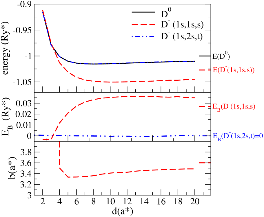
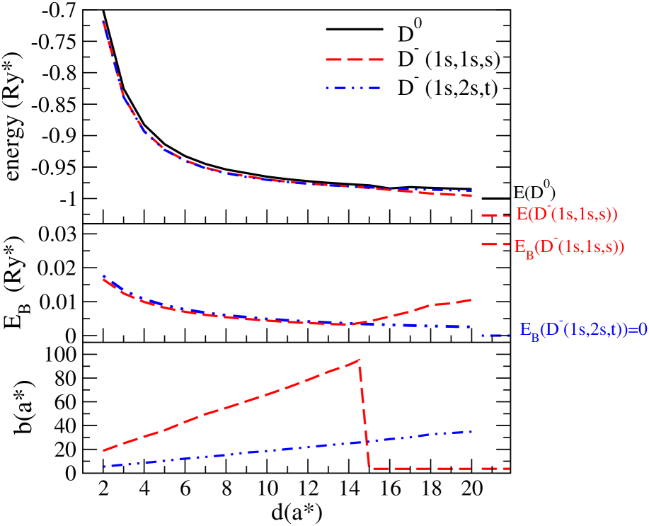
In Figs. 3 and 4, we plot and the binding energy assuming a trial wave-function with variational parameters and , for and respectively. The radius of the inner orbital is while , the radius of the outer orbital, depends very strongly on and and is shown in Figs. 3(c) and 4(c). We have done calculations for several values of , ranging from to . The general trends and qualitative behavior of the calculated quantities versus distance are the same for all (effective barrier dominated by the metallic character of the interface materials), which differ from the also general behavior of (effective barrier dominated by the insulator material). For (illustrated for the particular case of in Fig. 3), is not bound for small (for in the case of ). For larger ’s, the binding energy is slightly enhanced from the bulk value. The radius of the outer orbital is very close to the bulk value for . For (illustrated by in Fig. 4), is bound at all distances , though the binding energy is smaller than in bulk. The radius of the outer orbital is very large and increases linearly with up to [see Fig. 4 (c)]. For larger , is suddenly reduced to its bulk value. This abrupt behavior of the that minimizes the energy is due to two local minima in the energy versus : for the absolute minimum corresponds to a very large (but finite) orbital radius while for the absolute minimum crosses over to the other local minimum, at . As increases from the smallest values and increases up to the discontinuous drop, a “kink” in the D- binding energy is obtained at the crossover point [see Fig. 4 (b)], changing its behavior from a decreasing to an increasing dependence on towards the bulk value as .
III.2 Charging energy: experimental results
The charging energy of shallow dopants can be obtained by using the combined results of photoconductivity experiments to determine the binding energy Dean et al. (1967) and direct optical spectroscopy to determine the binding of the state. Ramdas and Rodriguez (1981) It was shown recently that the charging energy in nanostructures can be obtained directly from charge transport spectroscopy at low temperature. Sellier et al. (2006) Single dopants can be accessed electronically at low temperature in deterministically doped silicon/silicon-dioxide heterostructures Morello et al. (2010) and in small silicon nanowire field effect transistors (FinFETs), where the dopants are positioned randomly in the channel. Sellier et al. (2006); Lansbergen et al. (2008); Pierre et al. (2009) Here we will focus in particular on data obtained using the latter structures. Sellier et al. (2006); Lansbergen et al. (2008)
FinFET devices in which single dopant transport have been observed typically consist of crystalline silicon wire channels with large patterned contacts fabricated on silicon-on-insulator. Details of the fabrication can be found in Ref. Sellier et al., 2006. In this kind of samples, few dopants may diffuse from the source/drain contacts into the channel during the fabrication modifing the device characteristics both at room Pierre et al. (2009) and low temperatures. Sellier et al. (2006); Lansbergen et al. (2008); Pierre et al. (2009) In some cases, subthreshold transport is dominated by a single dopant. Lansbergen et al. (2008)
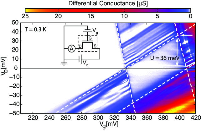
Low temperature transport spectroscopy relies on the presence of efficient Coulomb blockade with approximately zero current in the blocked region. This requires the thermal energy of the electrons, , to be much smaller than , a requirement that is typically satisfied for shallow dopants in silicon at liquid helium temperature and below, i.e. . At these temperatures the current is blocked in a diamond-shaped region in a stability diagram, a color-scale plot of the current – or differential conductance – as a function of the source/drain, , and gate voltage, .
In Fig. 5, the stability diagram of a FinFET with only one As dopant in the conduction channel is shown. At small bias voltage (), increasing the voltage on the gate effectively lowers the potential of the donor such that the different donor charge states can become degenerate with respect to the chemical potentials in the source and drain contacts and current can flow. The difference in gate voltage between the DD0 and DD- degeneracy points (related to the charging energy) depends, usually in good approximation, linearly on the gate voltage times a constant capacitive coupling to the donor. Sellier et al. (2006) Generally a more accurate and direct way to determine the charging energy is to determine the bias voltage at which the Coulomb blockade for a given charge state is lifted for all gate voltages, indicated by the horizontal arrow in Fig. 5. This method is especially useful when there is efficient Coulomb blockade. For the particular sample shown in Fig. 5, meV. This is similar to other reported values in the literature Sellier et al. (2006); Lansbergen et al. (2008); Pierre et al. (2009) ranging from to meV. There is therefore a strong reduction in the charging energy compared to the bulk value meV. The ratio between the observed and the bulk value is .
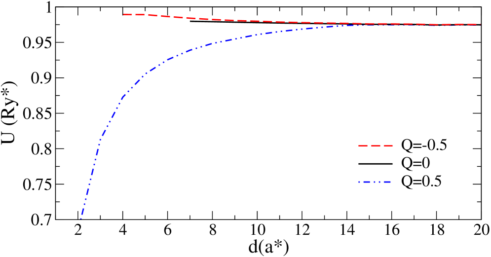
Theoretically, we can extract the charging energy from the results in Figs. 3 and 4. The results are shown as a function of for , , and in Fig. 6. A reduction of the charging energy of the order of the one observed occurs at for (only is shown in the figure). Therefore, the experimentally observed behavior of is consistent with a predominant influence of the metallic gates material in the D- energetics. On the other hand, for , is slightly enhanced as decreases and, for the smallest values of considered, the outer orbital is not bound. At very short distances , the difference in behavior between the insulating barrier () and the barrier with more metallic character () is in the interaction between each electron and the other electron’s image, which is repulsive in the former case and attractive in the latter. Although this interaction is small, it is critical to lead to a bound for and an unbound for at very short .
III.3 first excited state.
It is well established that in 3 dimensions (with no magnetic field applied) there is only one bound state of .Hill (1977); Larsen and McCann (1992) Motivated by the significant changes in the ground state energy produced by nearby interfaces, we explore the possibility of having a bound excited state in a double-charged single donor. Like helium, we expect the first excited state to consist of promoting one electron to the orbital. The spin triplet state (which is orthogonal to the singlet ground state) has a lower energy than . Bransden and Joachain (2003) As a trial wave-function for we use the antisymmetrized product of the two orbitals and and multiply by to fulfill the boundary condition, namely,
| (8) | |||||
with and variational parameters and a normalization factor. Note that, for a particular value of , the outer electron in a orbital would have a larger effective orbital radius than in a orbital due to the different form of the radial part.
For , the outer orbital is not bound and the energy reduces to that of (see Fig. 3). Surprisingly, for the state is bound and, as increases, tends very slowly to the energy as shown in Fig. 4. Moreover, its binding energy is roughly the same as the ground state for , another unexpected result. The existence of a bound triplet state opens the possibility of performing coherent rotations involving this state and the nearby singlet ground state.
IV Discussions and conclusions
Our model for centers involves a number of simplifications: (i) the mass anisotropy is not included; (ii) the multivalley structure of the conduction band of Si is not considered; (iii) correlation terms in the trial wave-function are neglected. These assumptions aim to decrease the number of variational parameters while allowing many of the integrals to be solved analytically.
Qualitatively, regarding assumption (i), it has been shown that the mass anisotropy inclusion gives an increase of the binding energy for both and (see Ref. Inoue et al., 2008); regarding (ii), inclusion of the multivalley structure of the conduction together with the anisotropy of the mass would lead to an enhancement of the binding energy of due to the possibility of having intervalley configurations in which the electrons occupy valleys in ’perpendicular’ orientations, (with perpendicularly oblated wave-functions), thus leading to a strong reduction of the electron-electron repulsive interaction. Larsen (1981); Inoue et al. (2008) Regarding point (iii), more general trial wave-functions for have been proposed in the literature. For example, the one suggested by Chandrasekar models correlation effects by multiplying Eq. 4 by a factor, , Chandrasekhar (1944) where is an additional variational parameter. In the bulk, the effect of this correlation factor is to increase the binding energy of from if (our case) to . Bethe and Salpeter (2008) We conclude that all three simplifications assumed in our model lead to an underestimation of the binding energy of , thus, the values reported here are to be taken as lower bounds for it.
As compared to experiments, an important difference with respect to the theory is that we are assuming a flat-band condition while the actual devices have a built-in electric field due to band-bending at the interface between the gate oxide and the p-doped channel. Lansbergen et al. (2008); Rahman et al. (2009) If an electric field were included, the electron would feel a stronger binding potential (which results from the addition of the donor potential and the triangular potential well formed at the interface) leading to an enhancement of the binding energy of and (with an expected strong decrease of the electron-electron interaction in this case for configurations with one electron bound to the donor at and the other pulled to the interface at ).
The presented results are dominated by the presence of a barrier, which constrains the electron to the region, and the modification of the screening due to the charge induced at the interface, a consequence of the dielectric mismatch between Si and the barrier material. This is included by means of image charges. Effects of quantum confinement and dielectric confinementDelerue and Lannoo (2004); Diarra et al. (2007) are not considered here: we believe these are not relevant in the FinFETs under study. Although the conduction channel is very narrow ( nm2)Sellier et al. (2007) the full cross section of the Si wire is various tens of nm and quantum and dielectric confinement is expected to be effective for typical device sizes under nm. Both quantum and dielectric confinement lead to an enhancement of the binding energy with respect to the bulk, which is the opposite to what we obtain for small .
Neutral double donors in Si, such as Te or Se, have been proposed for spin readout via spin-to-charge conversion Kane et al. (2000) and for spin coherence time measurements.Calderón et al. (2007) The negative donor also constitutes a two-electron system, shallower than Te and Se. In this context, investigation of the properties of shallow donors in Si affecting quantum operations as, for example, their adequacy for implementing spin measurement via spin-to-charge conversion mechanism, Kane et al. (2000); Koppens et al. (2005) deserve special attention. Our theoretical study indicates that, very near an interface (for ), the stability of D- against dissociation requires architectures that yield effective dielectric mismatch , a requirement for any device involving operations or gates based on D- bound states.
In conclusion, we have presented a comprehensive study of the effects of interface dielectric mismatch in the charging energy of nearby negatively charged donors in Si. In our study, the theoretical treatment is based on a single-valley effective mass formalism, while transport spectroscopy experiments were carried out in FinFET devices. The experiments reveal a strong reduction on the charging energy of isolated As dopants in FinFETs as compared to the bulk values. Calculations present, besides the charging energy, the binding energy of donor in three different charge states as a function of the distance between the donor and an interface with a barrier. The boundary problem is solved by including the charge images whose signs depend on the difference between the dielectric constant of Si and that of the barrier material [the dielectric mismatch, quantified by the parameter defined below Eq. (6)].
Typically, thin insulating layers separate the Si channel, where the dopants are located, from metallic gates needed to control the electric fields applied to the device. This heterostructured barrier leads to an effective screening with predominance of the metallic components, if compared to a purely SiO2 thick layer, for which . Assuming a barrier material with an effective dielectric constant larger than that of Si (in particular, corresponds to ), we obtain a reduction of the charging energy relative to at small , consistent with the experimental observation. We did not attempt quantitative agreement between presented values here, but merely to reproduce the right trends and clarify the underling physics. It is clear from our results that more elaborate theoretical work on interface effects in donors, beyond the simplifying assumptions here, should take into account the effective screening parameter as a combined effect of the nearby barrier material and the adjacent metallic electrodes. From our calculations and experimental results, we conclude that the presence of metallic gates tend to increase above , leading to and reducing the charging energies.
Acknowledgements.
M.J.C. acknowledges support from Ramón y Cajal Program and FIS2009-08744 (MICINN, Spain). B.K. acknowledges support from the Brazilian entities CNPq, Instituto Nacional de Ciencia e Tecnologia em Informação Quantica - MCT, and FAPERJ. J.V., G.P.L, G.C.T and S.R. acknowledge the financial support from the EC FP7 FET-proactive NanoICT projects MOLOC (215750) and AFSiD (214989) and the Dutch Fundamenteel Onderzoek der Materie FOM. We thank N. Collaert and S. Biesemans at IMEC, Leuven for the fabrication of the dopant device.References
- Kane (1998) B. E. Kane, Nature 393, 133 (1998).
- Vrijen et al. (2000) R. Vrijen, E. Yablonovitch, K. Wang, H.-W. Jiang, A. Balandin, V. Roychowdhury, T. Mor, and D. DiVincenzo, Phys. Rev. A 62, 012306 (2000).
- Skinner et al. (2003) A. J. Skinner, M. E. Davenport, and B. E. Kane, Phys. Rev. Lett. 90, 087901 (2003).
- Barrett and Milburn (2003) S. D. Barrett and G. J. Milburn, Phys. Rev. B 68, 155307 (2003).
- Hollenberg et al. (2004) L. C. L. Hollenberg, A. S. Dzurak, C. Wellard, A. R. Hamilton, D. J. Reilly, G. J. Milburn, and R. G. Clark, Phys. Rev. B 69, 113301 (2004).
- Calderón et al. (2006) M. J. Calderón, B. Koiller, X. Hu, and S. Das Sarma, Phys. Rev. Lett. 96, 096802 (2006).
- MacMillen and Landman (1984) D. MacMillen and U. Landman, Phys. Rev. B 29, 4524 (1984).
- Calderón et al. (2007) M. J. Calderón, B. Koiller, and S. Das Sarma, Phys. Rev. B 75, 125311 (2007).
- Delerue and Lannoo (2004) C. Delerue and M. Lannoo, Nanostructures. Theory and modelling (Springer-Verlag (Berlin), 2004).
- Diarra et al. (2007) M. Diarra, Y.-M. Niquet, C. Delerue, and G. Allan, Phys. Rev. B 75, 045301 (2007).
- Björk et al. (2009) M. T. Björk, H. Schmid, J. Knoch, H. Riel, and W. Riess, Nature Nanotechnology 4, 103 (2009).
- Voyles et al. (2002) P. M. Voyles, D. A. Muller, J. L. Grazui, P. H. Citrin, and H.-J. L. Grossmann, Nature 416, 827 (2002).
- Shinada et al. (2005) T. Shinada, S. Okamoto, T. Kobayashi, and I. Ohdomari, Nature (London) 437, 1128 (2005).
- Pierre et al. (2009) M. Pierre, R. Wacquez, X. Jehl, M. Sanquer, M. Vinet, and O. Cueto, Nature Nanotechnology 5, 133 (2009).
- Sellier et al. (2006) H. Sellier, G. P. Lansbergen, J. Caro, S. Rogge, N. Collaert, I. Ferain, M. Jurczak, and S. Biesemans, Phys. Rev. Lett. 97, 206805 (2006).
- Lampert (1958) M. A. Lampert, Phys. Rev. Lett. 1, 450 (1958).
- Taniguchi and Narita (1976) M. Taniguchi and S. Narita, Solid State Communications 20, 131 (1976).
- Larsen and McCann (1992) D. M. Larsen and S. Y. McCann, Phys. Rev. B 45, 3485 (1992).
- Shi et al. (1995) J. M. Shi, F. M. Peeters, and J. T. Devreese, Phys. Rev. B 51, 7714 (1995).
- Pekeris (1962) C. L. Pekeris, Phys. Rev. 126, 1470 (1962).
- Hill (1977) R. Hill, Phys. Rev. Lett. 38, 643 (1977).
- Bethe and Salpeter (2008) H. Bethe and S. Salpeter, Quantum mechanics of one and two electron atoms (Dover publications, NY, 2008).
- Ramdas and Rodriguez (1981) A. Ramdas and S. Rodriguez, Reports on Progress in Physics 44, 1297 (1981).
- Slachmuylders et al. (2008) A. F. Slachmuylders, B. Partoens, F. M. Peeters, and W. Magnus, Appl. Phys. Lett. 92, 083104 (2008).
- Dean et al. (1967) P. Dean, J. Haynes, and W. Flood, Physical Review 161, 711 (1967).
- Morello et al. (2010) A. Morello, J. J. Pla, F. A. Zwanenburg, K. W. Chan, H. H. M. Mottonen, C. D. Nugroho, C. Yang, J. A. van Donkelaar, A. Alves, D. N. Jamieson, et al., arXiv:1003.2673 (2010).
- Lansbergen et al. (2008) G. P. Lansbergen, R. Rahman, C. J. Wellard, I. Woo, J. Caro, N. Collaert, S. Biesemans, G. Klimeck, L. C. L. Hollenberg, and S. Rogge, Nature Physics 4, 656 (2008).
- Bransden and Joachain (2003) B. Bransden and C. Joachain, Physics of atoms and molecules (Prentice Hall, 2003).
- Inoue et al. (2008) J.-i. Inoue, J. Nakamura, and A. Natori, Phys. Rev. B 77, 125213 (2008).
- Larsen (1981) D. M. Larsen, Phys. Rev. B 23, 5521 (1981).
- Chandrasekhar (1944) S. Chandrasekhar, Rev. Mod. Phys. 16, 301 (1944).
- Rahman et al. (2009) R. Rahman, G. P. Lansbergen, S. H. Park, J. Verduijn, G. Klimeck, S. Rogge, and L. C. L. Hollenberg, Phys. Rev. B 80, 165314 (2009).
- Sellier et al. (2007) H. Sellier, G. P. Lansbergen, J. Caro, S. Rogge, N. Collaert, I. Ferain, M. Jurczak, and S. Biesemans, Appl. Phys. Lett. 90, 073502 (2007).
- Kane et al. (2000) B. E. Kane, N. S. McAlpine, A. S. Dzurak, R. G. Clark, G. J. Milburn, H. B. Sun, and H. Wiseman, Phys. Rev. B 61, 2961 (2000).
- Calderón et al. (2007) M. Calderón, B. Koiller, and S. Das Sarma, Phys. Rev. B 75, 161304(R) (2007).
- Koppens et al. (2005) F. H. L. Koppens, J. A. Folk, J. M. Elzerman, R. Hanson, L. H. W. van Beveren, I. T. Vink, H. P. Tranitz, W. Wegscheider, L. P. Kouwenhoven, and L. M. K. Vandersypen, Science 309, 1346 (2005).