Tunable bandgaps and excitons in doped semiconducting carbon nanotubes made possible by acoustic plasmons
Abstract
Doping of semiconductors is essential in modern electronic and photonic devices. While doping is well understood in bulk semiconductors, the advent of carbon nanotubes and nanowires for nanoelectronic and nanophotonic applications raises some key questions about the role and impact of doping at low dimensionality. Here we show that for semiconducting carbon nanotubes, bandgaps and exciton binding energies can be dramatically reduced upon experimentally relevant doping, and can be tuned gradually over a broad range of energies in contrast to higher dimensional systems. The later feature is made possible by a novel mechanism involving strong dynamical screening effects mediated by acoustic plasmons.
Nanomaterials have been lauded for their promise in electronic and photonic applications Avouris . Quite often, the imagined nanodevices rely on analogies with those based on bulk semiconductors. However, the true potential of nanomaterials lies in the exploitation of their unique properties to realize entirely new device concepts. In particular, approaches for externally controlling their electronic and optical properties would enable new strategies for device design.
Here we propose that such control is possible in carbon nanotubes (CNTs) through electrostatic doping. We find that quasiparticle (QP) band gaps and exciton binding energies can be reduced dramatically by hundreds of meVs upon doping, and yet prominent optical absorption features shift by relatively small amounts. Furthermore, we show that doping has a unique influence on CNT exciton properties: in contrast to bulk excitons, bound excitons in semiconducting CNTs are not quenched by doping and their binding energy can be tuned gradually even at very high doping. These features arise due to the presence of acoustic plasmons and their impact on dynamical screening.
We utilize a many-body ab initio approach Hybertsen ; Rohlfing ; Spataru1 to calculate the electronic and optical properties of electrostatically doped semiconducting CNTs. We focus on the semiconducting (10,0) CNT, with diameter , and perform ab initio calculations note2 at zero doping and for a free carrier concentration . We use the GW approach Hybertsen to obtain QP properties near the point and solve the Bethe-Salpeter (BS) equation for the excitonic effects Rohlfing . Applying this approach to doped CNTs necessitates careful consideration because of the presence of acoustic plasmons, a unique feature of low-dimensionality materials Hu ; Lin .
Indeed, in quasi-1D systems such as CNTs, electron gas and tight-binding models predict “acoustic” plasmons, whose energies approach zero in the long wavelength limit . Our ab initio calculations also reveal these plasmons in doped CNTs truncate : Fig. 1a shows the inverse dielectric function of the (10,0) CNT at = 0.6 holes/nm. The peak in Im signals a low-energy plasmon, which gives rise to a transition in Re between a very small value at zero energy and a value close to 1 above the plasmon energy, i.e. a transition between metallic-like and semiconducting-like screening Spataru2 . These acoustic plasmons span a broad range of energies, as seen in Fig. 1b, and dynamical screening effects due to them are very important for both QPs and excitons and cannot be neglected or simply integrated out.
To include these dynamical screening effects during the calculations we modify methods previously applied in the context of doped bulk semiconductors Oschlies . In the undoped case, optical plasmons in CNTs have energies above eV Kramberger , and their contributions is taken into account through the Generalized Plasmon Pole (GPP) approximation Hybertsen . In the doped case, GPP alone does not describe satisfactorily dynamical effects from acoustic plasmons and the screening is evaluated instead from , where is the dielectric function of the intrinsic semiconductor for which we make use of the GPP approximation and is obtained within the Random Phase Approximation.
Dynamical effects are included in the BS calculations by an effective dielectric screening that depends self-consistently on the binding energy of the exciton Strinati . Taking advantage of the fact that for the excitons considered here most of the corresponding electron-hole transitions have energies close to the onset of the electron-hole continuum, and neglecting finite lifetime effects, one can write to first order in dynamical effects note1 :
| (1) |
When low-energy plasmons are absent, the commonly used static approximation is obtained by retaining the first term on the r.h.s. of Eq. (1). The second term captures dynamical effects due to acoustic plasmons (we neglect dynamical effects due to optical plasmons during the BS calculations in both undoped and doped cases). Smaller, higher order corrections in dynamical effects (not shown in Eq. ) due to acoustic plasmons are included as well in our calculations.
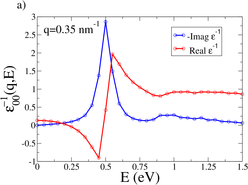
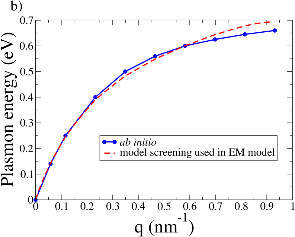
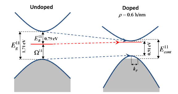
Fig. 2 shows a sketch of the calculated QP bands and exciton level associated with the lowest prominent optical transition (), before and after doping, where the energy scale has been preserved between the two cases. The quantities of interest are the bandgap and the exciton binding energy . It is clear from this figure that the bandgaps and exciton binding energies are significantly reduced by doping. In fact, at this doping (), is reduced by 800 meV, while is reduced by 590 meV. Both of these changes are large by any measure; in particular we estimate that band gap renormalization (BGR) is about an order of magnitude larger than in typical bulk semiconductors at the same doping Abram . The QP bands and exciton level associated with the second lowest prominent optical transition (, not shown in Fig. 2) also suffer from a significant bandgap reduction of 130 meV note3 , and a decrease of the exciton binding energy by 240 meV. Moreover, doping leads to an important 40% reduction in the effective mass at the valence band maximum for .
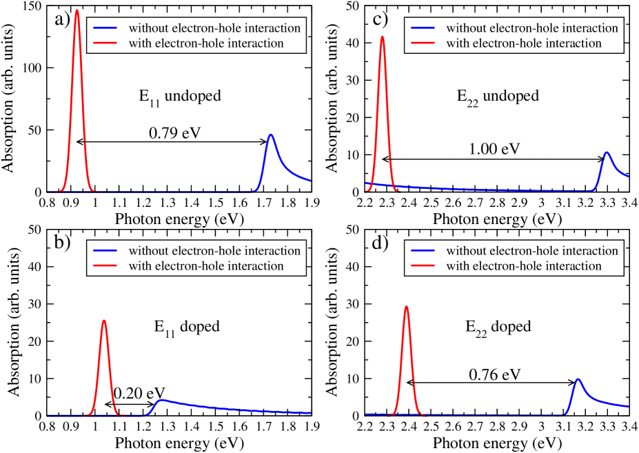
The excitonic effects are presented in more detail in Fig. 3, where the optical absorption spectra for light polarized along the tube axis is calculated in two ways. The blue lines are obtained neglecting the electron-hole interaction, with the corresponding onset energies indicating the electron-hole continua. The red lines show the correct absorption spectra obtained with the electron-hole interaction included. As each bound exciton requires a separate self-consistent calculation in the doped case, we have focused on the lowest energy bright exciton associated with each of the and continua.
In the undoped case, the and excitons show very large binding energies: and . As discussed above, upon doping, a dramatic change in excitonic properties occurs. As seen in Fig. 3b, suffers a decrease of eV to , while the corresponding renormalization is 0.24 eV (see Fig. 3d). While both the and excitons are affected by the change in dielectric screening, the exciton renormalizes more because it is affected by the bleaching of transitions. We also note from Fig. 3b a six-fold reduction in the oscillator strength of the exciton, in good accord with recent photo-luminescence measurements Steiner which assigned a factor of five in the drop of the exciton radiative decay rate of a 1.4 nm diameter CNT [for an estimated maximum doping ].
Our ab initio results suggest large changes in bandgap and exciton properties upon doping note4 . This could lead, for example, to engineering of CNT optoelectronic devices by electrostatic control; but taking advantage of these new features requires robust control of doping-induced properties. Because our many-body ab initio calculations are extremely demanding, exploring the tailoring over a broad range of doping is not possible. Therefore, we developed a compact model for excitons in doped CNTs based on an effective mass (EM) approach Sham .
Our EM model seeks to describe the binding energy and envelope function of excitons in CNTs taking advantage of their large spatial extent along the tube axis relative to inter-atomic distances. The effective interaction between the electron and hole composing an exciton depends on via [see Eq. (1)] the dielectric function , where P is the irreducible polarizability. Our EM approximation assumes that is localized on a cylindrical tubule with radius R, and that local field effects along the tube axis can be neglected. Noting that only the L=0 component of the angular momentum L is relevant for screening effects in excitons composed of electron-hole transitions between bands of same L, one replaces with . Relevant dynamic effects are included via , where describes intraband transitions within parabolic band approximation Hu , and represents the interband transitions for the intrinsic semiconductor. (We keep transitions from the top of valence band to conduction states as we found that they make very small contributions.) is extracted from ab initio calculations for the intrinsic polarizability () by imposing that and yield the same average along the radial direction over one unit cell. In Fourier space this reads: , where is the cross-sectional area of the unit cell considered in the ab initio case. The ability of our model -free of any adjustable parameters- in describing dynamical screening effects from acoustic plasmons is demonstrated in Fig. 1b.
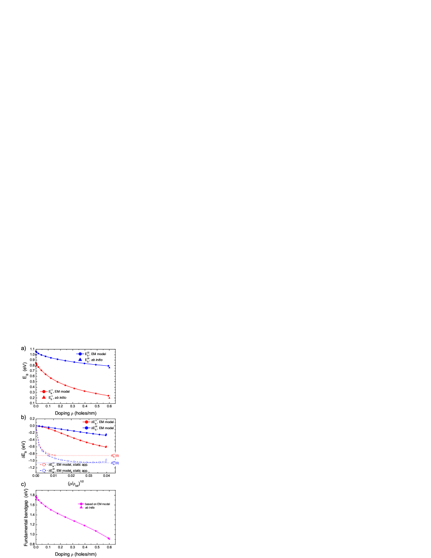
Fig. 4a shows the EM results for and extended to carrier densities as small as hole/800 nm (in terms of number of holes per atom, this corresponds to in typical bulk semiconductors, i.e., approximately the degenerate limit). Comparison with ab initio results illustrates the high accuracy of our EM model. Fig. 4b shows that with good approximation, , which we found to be a signature of acoustic plasmons. A similar trend is found for , where deviations from the behavior are more pronounced due to bleaching of transitions. More importantly, the mild dependence on doping should be contrasted to that in higher dimensional semiconductors where, at equivalent doping levels, excitons are either quenched Schweizer or the dependence on doping is exponential Gubarev , giving poor control over optical properties.
The large change in exciton binding energy combined with the mild dependence on doping implies that excitonic properties in CNTs can be efficiently controlled through doping. The origin of this feature lies in the presence of acoustic plasmons. To emphasize this point, Fig. 4b also shows EM results for exciton binding energies within the static approximation, i.e. without proper inclusion of dynamical effects due to acoustic plasmons. In this case, binding energies drop exponentially with doping, much like is observed in two-dimensional materials Gubarev ; moreover, the exciton gets quenched beyond hole/15 nm. The importance of acoustic plasmons is readily seen within our model and from Eq. (1), which can be shown to yield: . For long wavelengths where , one has , as opposed to the static approximation result . The difference between these two values can be orders of magnitude depending on q.
We obtain the QP fundamental bandgap versus doping using our exciton EM model and our many-body ab initio results for optical properties. Indeed, we can write where is the exciton excitation energy and (see Fig. 2). We calculate the doping dependence of from , with the reduced exciton mass obtained at various doping levels by interpolating the values from many-body ab initio calculations at and . Furthermore, we find from our ab initio calculations at that only increases by eV upon doping (similarly for ), a result of cancelation between self-energy corrections and excitonic effects Burstein . The smallness of these shifts is in excellent agreement with measurements of the absorption peak of a 1.4 nm diameter CNT Steiner , showing a red-shift of 20 meV at . Therefore, with little expected error, we assume a linear dependence of on doping, and plot in Fig. 4c the fundamental bandgap versus doping; the trend indicates that BGR can also be tuned gradually over a broad energy range.
The giant BGR discussed here is in agreement with recent experimental results Lee that combined photocurrent spectroscopy with transport measurements: for a 1.5 nm diameter CNT with QP band gap of 0.91 eV at zero doping, a BGR of 0.54 eV was deduced at a doping density of 0.7 electrons/nm.
In conclusion, we have shown that doping has a profound and unique impact on the electronic and optical properties of semiconducting CNTs, and that dynamical effects from acoustic plasmons are essential to capture these effects. Our study indicates that bandgaps and exciton binding energies in CNTs can be tuned significantly and gradually by electrostatic doping, establishing a new framework for the understanding and design of CNT-based devices. We expect that similar control will be possible in a broad range of nanomaterials.
Sandia is a multiprogram laboratory operated by Sandia Corporation, a Lockheed Martin Company, for the United States Department of Energy’s National Nuclear Security Administration under Contract DE-AC04-94AL85000. Work supported by the Lockheed Martin Shared Vision program.
* Corresponding author. E-mail: cdspata@sandia.gov
References
- (1) P. Avouris, Z. Chen, and V. Perebeinos, Nature Nanotech. 2, 605 (2007); W. Lu and C.M. Lieber, Nature Mater. 6, 841 (2007); P. Pauzauskie and P. Yang, Materials Today 9, 36 (2006); X. Wang et al., Phys. Rev. Lett. 100, 206803 (2008); I.V. Bondarev, L.M. Woods and K. Tatur, Phys. Rev. B, 80, 085407 (2009).
- (2) M.S. Hybertsen and S.G. Louie, Phys. Rev. B 34, 5390 (1986).
- (3) M. Rohlfing and S.G. Louie, Phys. Rev. B 62, 4927 (2000).
- (4) C.D. Spataru et al., Phys. Rev. Lett. 92, 077402 (2004).
- (5) Ground-state properties are obtained within within Density Functional Theory in Local Density Approximation using ab initio pseudopotentials in a plane-wave basis. The 1D Brillouin zone is sampled by at least 128 k-points (up to 512 k-points during the ab initio excited state calculations).
- (6) G.Y. Hu and R.F. O’Connell, J. Phys.: Condens. Matter 2, 9381 (1990); O. Sato et al., Phys. Rev. B 48, 1947 (1993).
- (7) M.F. Lin and F.L. Shyu, Physica B 292, 117 (2000).
- (8) To capture this acoustic character, it is critical to truncate periodic image interactions between tubes; see S. Ismail-Beigi, Phys. Rev. B 73, 233103 (2006).
- (9) C.D. Spataru et al., Appl. Phys. A 78, 1129 (2004); F. Léonard and J. Tersoff, Appl. Phys. Lett. 81, 4835 (2002).
- (10) A. Oschlies, R.W. Godby, and R.J. Needs, Phys. Rev. B 51, 1527 (1995).
- (11) C. Kramberger et al., Phys. Rev. Lett. 100, 196803 (2008).
- (12) G. Strinati, Phys. Rev. Lett. 49, 1519 (1982); Phys. Rev. B 29, 5718 (1984).
- (13) We stress that , as an electron excited in a conduction band probes the density response of the system with a hole in the valence band Strinati .
- (14) R.A. Abram, G.J. Rees, and B.L.H. Wilson, Adv. Phys. 27, 799 (1978).
- (15) Within GPP alone during GW, and are reduced upon doping by meV and meV respectively.
- (16) M. Steiner et al., Nano Lett. 9, 3477 (2009).
- (17) Upon doping with 0.6 holes/nm, the exciton delocalizes over tens of nm along the tube axis (at zero temperature, the envelope function fall-off at large electron-hole separation is algebraic in the doped case, in contrast to the exponential decay in the undoped case) and acquires nodes separated by nm.
- (18) L.J. Sham and T.M. Rice, Phys. Rev. 144, 708 (1966).
- (19) H. Schweizer et al., Phys. Rev. Lett. 51, 698 (1983).
- (20) S.I. Gubarev et al., JETP Lett. 76, 575 (2002).
- (21) In bulk degenerate semiconductors, doping also leads to a blue-shift of the optical absorption edge (the Burstein-Moss effect), but in that case band filling is the largest effect; see E. Burstein, Phys. Rev. 93, 632 (1954).
- (22) J.U. Lee, Phys. Rev. B 75, 075409 (2007).