Pulse shape simulation for segmented true-coaxial HPGe detectors
Abstract
A new package to simulate the formation of electrical pulses in segmented true-coaxial high purity germanium detectors is presented. The computation of the electric field and weighting potentials inside the detector as well as of the trajectories of the charge carriers is described. In addition, the treatment of bandwidth limitations and noise are discussed. Comparison of simulated to measured pulses, obtained from an 18-fold segmented detector operated inside a cryogenic test facility, are presented.
keywords:
germanium detectors, segmentation, pulse shape simulationPACS:
23.40.-s , 24.10.Lx , 29.40.Gx , 29.40.Wk, , , , ,
1 Introduction
High purity germanium detectors, HPGeDs, are used in a wide variety of applications in particle and nuclear physics [1, 2]. The analysis of their pulse shapes, PSA, can be a powerful tool to determine event topologies, often a key to distinguish between signal and background events [3, 4, 5, 6]. In particular, the separation of events with energy depositions in one or multiple locations inside an HPGeD, single-site or multiple-site events, is of interest. Previous studies were often limited by the availability of clean event samples to train neural nets or to evaluate PSA [5, 6]. Therefore, simulated events reflecting a detailed understanding of the underlying processes are extremely valuable.
The interactions of radiation (, etc.) inside a semiconductor create electron-hole pairs. These charge carriers are separated by the electric field inside an HPGeD and drift towards the electrodes inducing time dependent charges. In most applications, charge sensitive amplifiers are used and the resulting pulses are sampled and digitized at a given frequency.
A new pulse shape simulation, PSS, package was developed. The geometry of an 18-fold,, segmented true-coaxial HPGeD [7] is implemented as default. The inner mantle has a radius of 5 mm, the outer of 37.5 mm. The length is 70 mm. This allows the comparison to data obtained from such a detector which was developed in connection to the GERDA [8] experiment. However, the simulation package itself is general and the geometry can easily be modified to accommodate any kind of germanium detector.
2 Simulation procedure
The package [9, 10] is separated into two parts, the calculation of the static properties of the HPGeD followed by the event by event simulation of the pulse development. The tabulation of the static properties is done once at the beginning of the simulation. It includes the electric field and the weighting potentials inside the detector.
The event by event simulation comprises the event topology and the development of the pulses in time-steps:
-
1.
Simulation of the interactions of particles with germanium. The output are individual positions with energy depositions, hits;
-
2.
Clustering of hits. According to the requirements of the simulation, hits can be clustered 111Hits closer to each other than the best hypothetical radial resolution of the detector, 1 mm, calculated as the speed of the charge carriers multiplied by the time resolution of the electronics, are clustered by default.. The position of the cluster is the bary-center of the original hits. The energy of the cluster, , is the sum of the energies of the original hits.
-
3.
Simulation of the drift of charge carriers in time-steps. For each cluster, only one point-like charge is considered. At each time-step the velocity of the charge is calculated using the electric field as tabulated;
-
4.
Calculation of the charges induced in the electrodes after each step;
-
5.
Simulation of experimental effects such as noise, bandwidth limitation, shaping times, etc..
The first step is done using the GEANT4 [11, 12] based simulation package MaGe [13], jointly developed by the GERDA and Majorana collaborations. The good agreement between MaGe and data obtained with segmented detectors was demonstrated previously [4].
All calculations are performed in cylindrical coordinates, and , with the origin at the center of the detector.
3 Electric field and weighting potentials
The electric field, , at a position inside an HPGeD depends on the geometry of the detector, the bias voltage, applied and the density of electrically active impurities, . It is considered static, calculated only once and tabulated for a reasonably spaced grid 222The default is a grid with a 1 mm spacing in and and a 2 degree spacing in .. The electric field at any position is calculated by interpolation.
For simple cases like a constant , can be calculated analytically solving Poisson’s equation , where is the space charge density is the dielectric constant. However, the electric field is always calculated numerically using the potential and the boundary conditions.
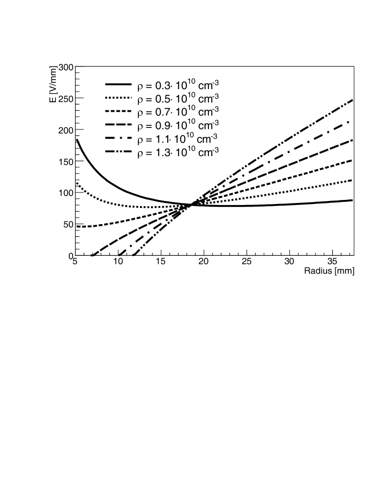
The boundary conditions for depend on . For the true-coaxial -type HPGeDs considered here, the potential is fixed to on the inner mantle, zero on the outer mantle and it floats on the end surfaces. The density determines and thereby affects the electric field inside an HPGeD. In the case of constant , the electric field only depends on . For this case, the output of the numerical calculation based on successive over-relaxation was tested against the numerical solution [10]. The deviations for realistic values of were found to be less than 0.6 % throughout the detector.
Figure 1 shows the calculated strength of the electric field as a function of for 3 kV and varying constant . This range of values is realistic for HPGeDs. For lower , the field is strong throughout the detector. For higher , the field is insufficient at small radii; a higher is needed.
As can vary up to a factor three between the two ends of a detector and might depend on , it is possible to specify a three dimensional distribution for .
The influence of any electrode on a given space-point inside the HPGeD is characterized by its weighting potential. This is defined according to Shockley-Ramo’s theorem [23, 24, 25] as the solution of Poisson’s equation for the boundary conditions that the potential on the electrode of interest equals unity and the potentials on all other electrodes equal zero. All weighting potentials are treated numerically like the electric field.
4 Drift of charge carriers
The drift of the charge carriers is calculated in time-steps, , for each point representing a cluster of hits as defined in Section 2. At each step the velocity is calculated using the electric field as tabulated. Between grid points a simple linear extrapolation is used for the electric field. Two different numerical methods are implemented to calculate the trajectories, the Euler method and the 4th Runge-Kutta method. The former is less computer time intensive, but is also less precise. However, for step-sizes ns, the resulting trajectories do not differ significantly [9].
The drift velocity of the charge carriers, for electrons and for holes, is calculated for each step using the electric field, , as tabulated:
| (1) |
where is the mobility [1] of electrons and holes, respectively.
Whether depend on the relative position of to the crystal axes is determined by the temperatures of the germanium crystal, , and of the charge carriers, . If , become numbers, and the drift velocities are directly proportional to the electric field. However, HPGeDs are normally operated at temperatures around 100 K and . In this case,the mobility becomes a complex tensor. Therefore, the simulation has to take the crystal structure into account and the calculation of becomes quite involved. The drift of the charge carriers is not any longer parallel to the electric field [14] for all .
The axes of the face-centered cubic structure of germanium crystals are characterized by Miller indices [15]. Cylindrical germanium detectors are produced with their axis aligned to the crystal axis [16]. This is implemented in the simulation. The axes and are in the -plane. Their relative position to the segment boundaries can be chosen freely, i.e. adjusted to the detector to be simulated.
The tensors are unfortunately not known. Special measurements along the crystallographic axes are used and parameterized. The results are combined to get results for any point in the crystal.
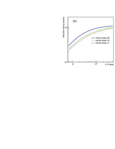
If the electric field is parallel to any of the principal crystallographic axes, the charge carriers will drift along this axis, because of the symmetric structure of the germanium crystal [14, 17]. The measured drift velocities [18, 19, 20], , along the axes and with for on and for on , respectively, are parametrized well [1, 19] for V/mm by
| (2) |
where , and are parameters determined by fitting. The parameters represent the linear relation between and at large and low . The parameters and are used to model the deviation from this linear relation at low lattice temperature and high electric fields.
The set of parameters given in [18] and validated for the drift of electrons [21] was used in the simulation presented here. The values are listed in Table 1.
| Carrier | Axis | |||
|---|---|---|---|---|
| 38536 | 53.8 | 0.641 | ||
| 38609 | 51.1 | 0.805 | ||
| 61215 | 18.2 | 0.662 | ||
| 61824 | 18.5 | 0.942 |
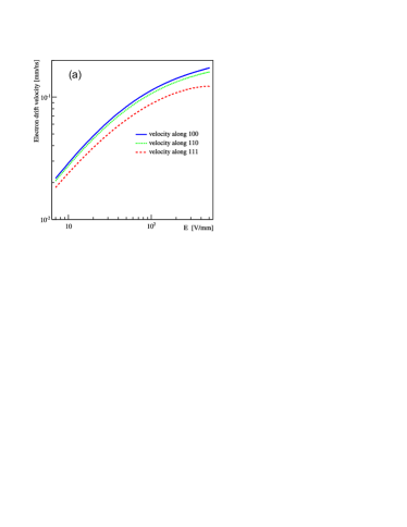
The drift velocities in any direction can be derived from the velocities along the and axes. The model used for the electron drift [19] is based on the idea that the conduction band in a germanium crystal reaches its minimal potential in regions around the four equivalent axes. Free electrons effectively only populate these regions. The probability density of free electrons in other regions can be ignored. The resulting drift velocities along the axis are shown together with the velocities for the and axes in Fig. 2(a).
The model used to calculate the hole drift velocities [18] in any direction is based on the idea that only the “heavy hole valence band” [22] is responsible for the anisotropy of the mobility. All other effects are neglected. A parameterization [18] is used to calculate the three components of the hole drift velocity at any position. The results for the axis together with the values for the and axes are shown in Fig. 2(b).
5 Trajectories
The results presented here were obtained with the Runge-Kutta method.
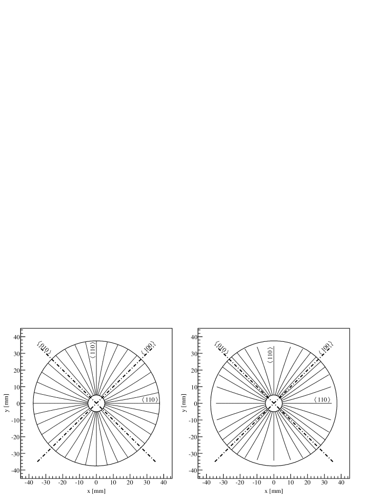
Figure 3 shows the trajectories of electrons and holes created at the outer and inner mantle, respectively. The step size was set to 1 ns and the total time simulated was 400 ns, = 3000 V and was constant through the volume. The trajectories are bent due to the crystal structure; this is called transverse anisotropy. The charge carriers are slower in the than in the direction; this is called longitudinal anisotropy. As holes are slower than electrons, the longitudinal anisotropy can be seen very clearly along where the holes do not reach the outer mantle within 400 ns.
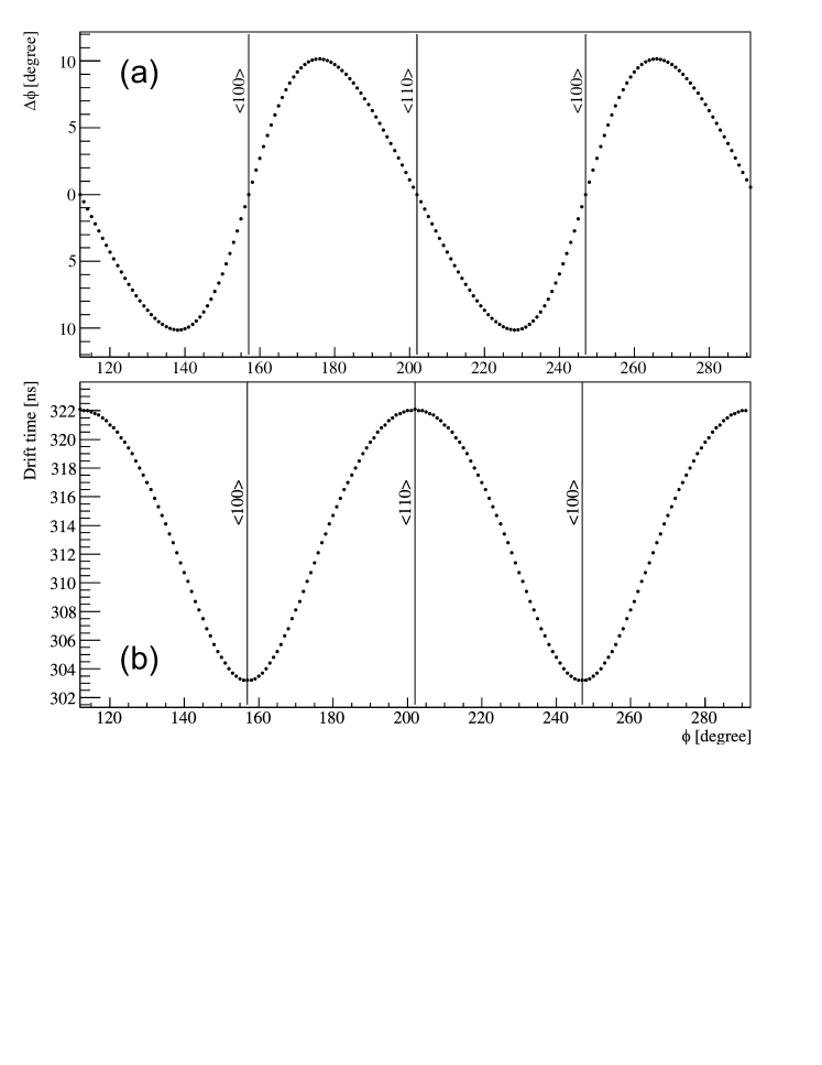
The transverse anisotropy is also demonstrated for electrons in fig. 4. It shows the displacement at the end of the drift and the total time needed for the drift as functions of the azimuthal angle at the start. Along the crystal axes and , . The drift time is minimal at and maximal at .
6 Charges induced on electrodes
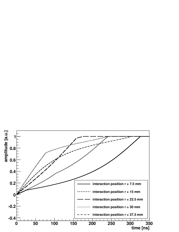
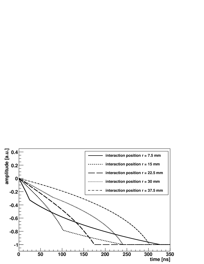
The electric signals are induced in the electrodes of a detector by the cumulative influence of moving electrons and holes. Shockley-Ramo’s Theorem [23, 24, 25] is used to calculate the time development of the induced charge or current in each electrode:
| (3) |
| (4) |
where is the electric charge carried by electrons or holes, and are the position and velocity vectors of electrons/holes as a function of time, and and are the weighting potentials and weighting fields.
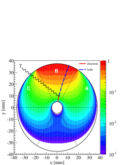
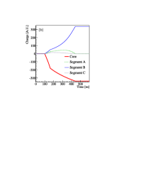
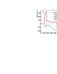
Figure 5a shows the weighting potential of a segment, B, with the indication of a photon interaction. The drift trajectories of holes and electrons are also indicated. Figures 5 (b) and (c) show the charges and currents induced on the electrodes of the segment with the interaction and its neighbors. The pulses induced in the neighboring segments are called mirror pulses. The amplitude of the mirror pulse induced in segment A is larger than the one in segment C since the trajectory is closer to segment A than C.
The charge pulses in segment B and the core show clear kinks at the time when the inwards drifting electrons reach the core electrode, i.e. the inner mantle. At that time the current pulses show maxima. The charge mirror-pulses do not show clear features at this time; the current mirror-pulses show more distinct features.
7 Influence of electronics
The most widely used amplification scheme is based on charge sensitive devices. The bandwidth is limited by the amplifiers and by the transmission cables. In order to account for the limited bandwidth and the decay time of the amplifier, the simulated pulses can be convoluted with a transfer function representing the readout electronics. In addition, Gaussian noise can be added to represent the noise of the system.
Figure 8 demonstrates the modification of a simulated pulse after folding in a decay time of s and a cut-off in bandwidth was 10 MHz. The noise level was set to 5 % of the pulse amplitude. These noise and band-width values are chosen to clearly demonstrates the effects.
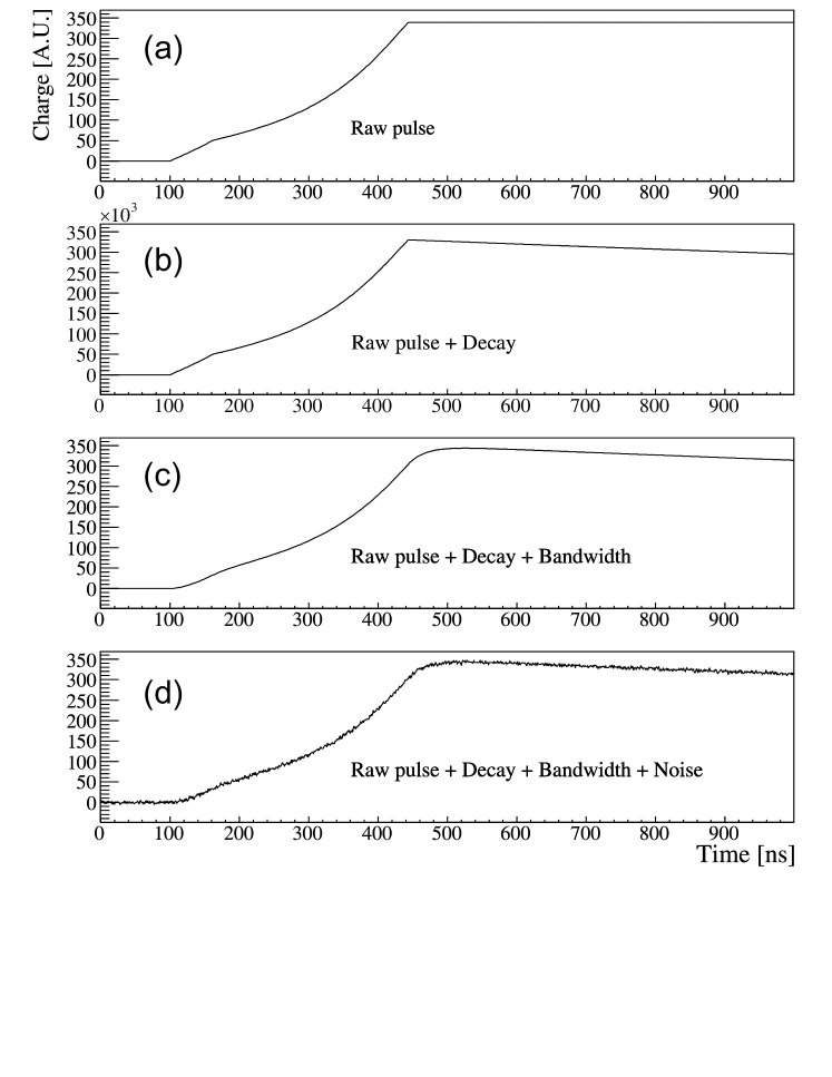
The decay-time of the preamplifier was chosen significantly larger than the length of the pulse. Therefore, mainly the plateau is affected. The cut-off in bandwidth smoothes the features of the pulse. The kink clearly visible at = 150 ns in Figure 8(b) is washed out significantly. The noise applied for Figure 8(d) makes the kink almost invisible.
8 Uncertainties of the simulation
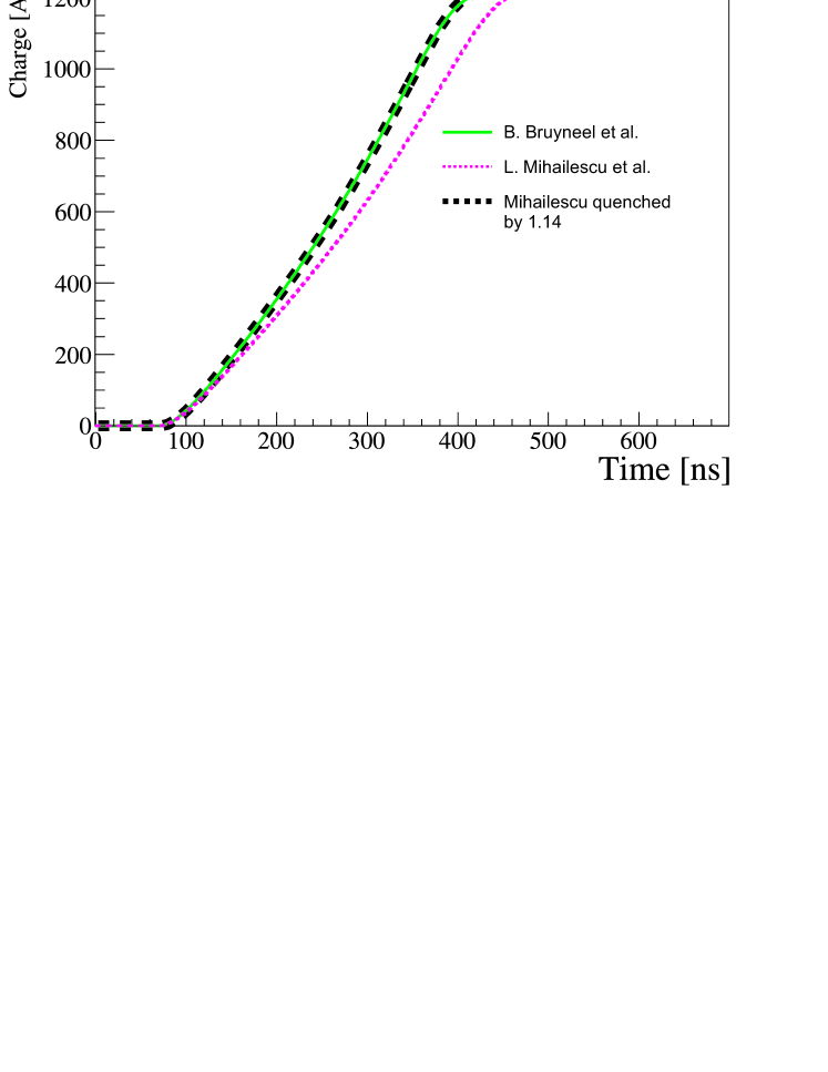
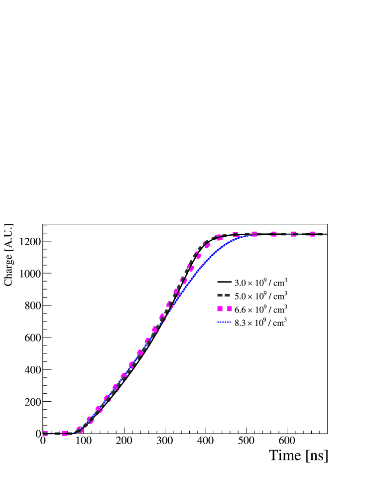
The output of the simulation depends critically on the input parameters used. A fundamental problem is the input concerning the mobilities. Figure 9 demonstrates how the pulses of events starting at the outer mantle and observed in the core are stretched if a different set [19] of input parameters for the electron mobility is chosen. At 3000 V and cm3, the pulse is 14 % longer than with the default input parameters [18]. However, a simple time scaling makes the pulses indistinguishable.
The length of a pulse is also strongly influenced by . This is demonstrated in Fig. 10. At 3000 V a change in from to cm3 has an effect on the core pulse of similar size than changing the mobility. In this case, the shape of the pulse is also modified; a simple time scaling does not make the pulses inddistinguishable. However, the effect is quite subtle and will be difficult to observe in real data. Unfortunately, the value of is generally not known to very high precision. In addition, it often varies up to a factor of three along . Therefore, it is unavoidable that pulses simulated for a particular detector or even detector section have to be scaled in time before more detailed comparisons to data can be made. Assuming a certain mobility, the length of the measured pulses can be used to derive the impurity density locally.
9 Comparison to data
The focus of the comparisons presented here is the drift of electrons. Therefore pulses as seen in the core electrode were used. Simulated pulses were compared to measured pulses produced by a well understood true-coaxial -type detector [7] irradiated with a collimated Europium source. The 122 keV line was used to study energy deposits close to the detector outer mantle. In this case, the holes are quickly absorbed by the electrodes on this outer mantle and mainly the drift of the electrons is relevant for the shape of the resulting pulses.
Two methods were used. Simulated pulses were either fitted to individual measured pulses or to averages of sets of pulses obtained in a given configuration. The latter was done to reduce the effects of noise.
9.1 Test environment
Figure 11 depicts the measurement setup. Three segments, numbered 13 to 15, of the middle layer of the detector were scanned in at . A collimated 75 kBq 152Eu source inside a copper collimator was used. The collimator pointed to the center of the detector and the spot had a 1 diameter of about 5 mm on the outer mantle of the detector. Details of the setup can be found elsewhere [7]. The operational voltage was 3 kV. The step size of the scan was 5∘ in segment 14 and 10∘ in segments 13 and 15. The uncertainty in was approximately . In total, 25 steps were made to cover 180∘ in azimuth. The pulses of the core and all segments were recorded. Events from the 122 keV -line were selected with a cut on the core energy of 2 of the energy resolution, i.e. about 4keV.

Simulations were done with the energy deposits located exactly on the outer mantle or distributed according to the interactions of the 122 keV photons from the 152Eu source. A constant cm3 was implemented. This is the average of the values given by the manufacturer for the top and the bottom of the detector which differ by a factor of two. The electric field was calculated for a bias voltage of kV. The measured orientation of the crystal axes was used in the simulation; the axis was set to , almost aligned with one boundary of segment 15.
An amplifier decay-time of 50 s and a cut-off in bandwidth of 37.5 MHz were implemented according to the specifications of the electronics system. Electronic noise was not added to the simulated pulses to simplify direct comparisons with individual measured pulses.
9.2 Fits to individual pulses
Simulated core pulses, , were fitted to measured pulses, , using three parameters only: the amplitude, , the time offset, , and the time scaling-factor :
| (5) |
Figure 12 shows a randomly selected core pulse at and the fit of the pulse generated for this angle. This position falls between the and the axes. The actual values of the parameters and have no relevance; they are not simulated in real units. The important parameter is which has a value of 0.90 0.01. The /dof = 184/146 = 1.3 for this fit is quite good.
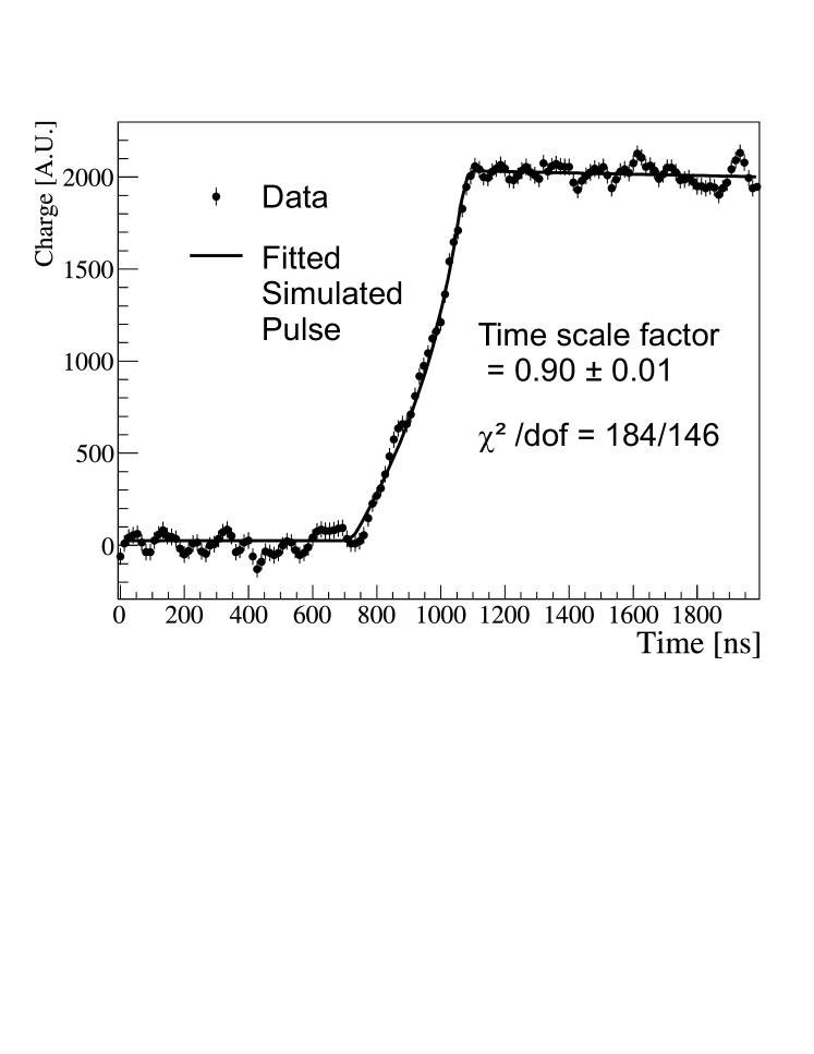
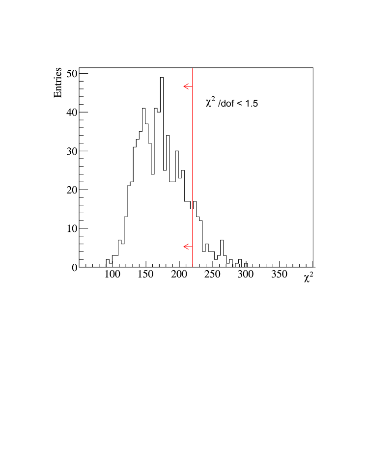
Fig. 13 shows the distribution of /dof values of all fits of pulses at . The average /dof = 174/146 = 1.2. In general, the quality of the fits is very good. This indicates that the simulation describes the general shape of the pulses very well. To determine an overall , a clean subset of measured pulses was selected by:
-
•
requiring , i.e. /dof , to eliminate background events which have probably more than one interaction in the segment;
-
•
rejecting events in which an intermittent DAQ problem might have affected the recording of the pulse.
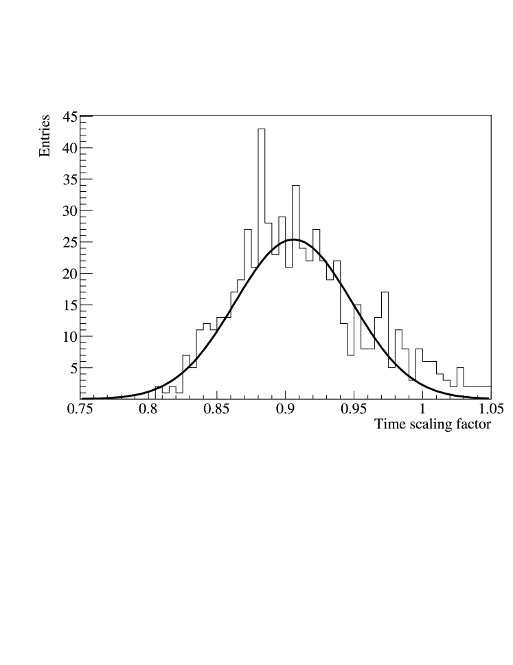
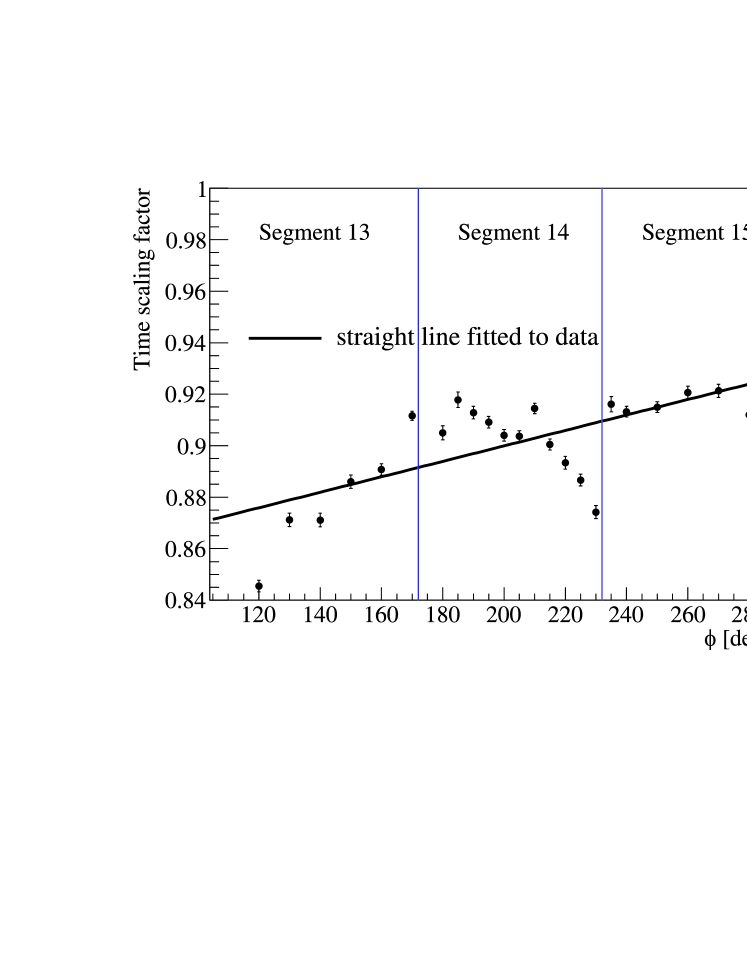
For each pulse, a value of was determined. Figure 14 shows the distribution of the time scaling-factors of the pulses at . The mean time scaling-factor of was extracted using a Gaussian fit. This was done for all positions in . Figure 15 shows the dependence of the mean time scaling-factors. The dotted vertical lines indicate the segment boundaries. A value of , independent of would be expected for a perfect simulation. However, considering the uncertainties in the input parameters, the level of agreement is quite astonishing. The time scaling-factors are systematically about 10 % low. This means that the simulated pulses are too short, indicating that the velocities of the electrons are overestimated. As discussed in section 8, this could be due to too high mobilities assumed or due to a slightly underestimated . It is impossible to distinguish the two possibilities at this point.
The dependence was fitted with a straight line. The absence of an oscillation pattern with a period of 90∘ shows that the longitudinal anisotropies introduced in the model describe reality in a satisfactory manner. The obvious dependence of on is difficult to explain. In germanium crystals, often depends on . If the central -axis of the original crystal is not identical with the -axis of the detector, a dependence of the observed average can result. A further investigation whether this effect can explain the about 5 % effect is under way.
9.3 Fits to averaged pulses
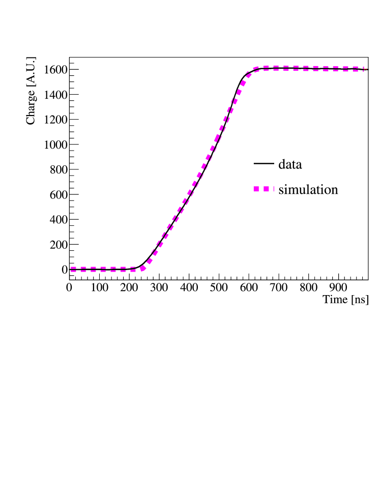
It would be interesting to carefully study the detailed shapes of individual pulses to distinguish between different sources of deviation between simulation and data. However, Fig. 12 shows that the noise level in this measurement does not allow this. In order to remove the effects of noise, the selected pulses at each scan position were averaged, even though the interaction points were spatially distributed according to the beam spot and the penetration depth of 122 keV photons.
The simulation was adjusted accordingly and the simulated pulses were also averaged. Averaged simulated pulses were fitted to averaged measured pulses. The result for is shown in Fig. 16. The fit yields . This is compatible to the mean observed before.
The /dof of the fit is 8. This is quite large. In Fig. 16, the deviations are also clearly visible. The simulated pulse has sharper edges most likely due to the overly optimistic cut of 37.5 MHz in the bandwidth; Figure 8 demonstrates how pulses get smoothed out by a cut in bandwidth of 10 MHz. At the very end of the pulse, the simulation shows an extra flattening. This would indicate that is slightly smaller than assumed. Nevertheless, the overall shape of the pulse is reproduced rather well and it will be tested soon, how well simulated pulses work as training sets for neural network based pulse shape analyses.
10 Summary and Outlook
A fully functional pulse shape simulation package for HPGe detectors was developed. It can easily be adapted to any common HPGe detector geometry. The results of the simulation are critically dependent on the input parameters. While some parameters are generic to germanium, the detailed properties of a detector like impurity concentration and axes orientation are also extremely important. Simulations have to be adjusted to each detector.
The longitudinal anisotropy of the elecron drift is correctly described by the simulation. Therefore the comparison of simulated to measured pulses can yield information about intrinsic detector properties like local variations of the impurity concentration.
The quality of the simulated pulses will be further studied and the simulation will be used as input to pulse shape analyses.
11 Acknowledgements
We would like to thank the members of the Monte Carlo group of the Majorana collaboration for their kind help in the analysis and cooperation in the programming.
References
- [1] G. F. Knoll, Radiation of Detection and Measurement third ed., (Wiley, New York 1999) 423.
- [2] J. Eberth and J. Simpson, Prog. Part. Nucl. Phys. 60(2008)283
- [3] S. R. Elliott et al., Nucl. Instr. Meth. A 558 (2006) 504.
- [4] I. Abt et al., Nucl. Instr. Meth. A 583 (2007) 332.
- [5] I. Abt et al., Eur. Phys. J. C 52 (2007) 19.
- [6] I. Abt et al., Eur. Phys. J. C 54 (2008) 425.
- [7] I. Abt et al., Nucl. Instr. Meth. A 577 (2007) 574.
- [8] I. Abt et al., arXiv:hep-ex/0404039v1 and S. Schönert et al., [GERDA Collab.], Nucl. Phys. Proc. Suppl. 145 (2005) 242.
- [9] J. Liu, phd-thesis, TU Munich, 2009
- [10] D. Lenz, phd-thesis, TU Munich, 2010
- [11] S. Agostinelli et al., [Geant4 Collab.], Nucl. Instr. Meth. A 506 (2003) 250.
- [12] J. Allison et al., IEEE Trans. Nucl. Sci. 53 (2006) 207.
- [13] Y. Chan et al., arXiv:0802.0860v1 [nucl-ex].
- [14] W. Sasaki and M. Shibuya, J. Phys. Soc. Japan 11 (1956) 1202.
- [15] N. W. Ashcroft and N. D. Mermin, Solid State Physics (Harcourt: New York, 1976)
- [16] Canberra France, private communication.
- [17] W. Sasaki, M. Shibuya and K. Mizuguchi, J. Phys. Soc. Japan 13 (1958) 456.
- [18] B. Bruyneel et al., Nucl. Instr. Meth. A 569 (2006) 764.
- [19] L. Mihailescu et al., Nucl. Instr. Meth. A 447 (2000) 350.
- [20] L. Reggiani et al., Phys. Rev. B 16 (1977) 2781.
- [21] B. Bruyneel, private communication.
- [22] E. M. Conwell, High field transport in semiconductors, Vol. 9 of Solid State Physics, (Academic Press, 1967).
- [23] E. Gatti, et. al., Nucl. Instr. Meth. 193 (1982) 651.
- [24] V. Radeka, Ann. Rev. Nucl. Part. Sci. 38 (1988) 217.
- [25] Z. He, Nucl. Instr. Meth. A 463 (2000) 250.