Inelastic Scattering and Current Saturation in Graphene
Abstract
We present a study of transport in graphene devices on polar insulating substrates by solving the Bolzmann transport equation in the presence of graphene phonon, surface polar phonon, and Coulomb charged impurity scattering. The value of the saturated velocity shows very weak dependence on the carrier density, the nature of the insulating substrate, and the low-field mobility, varied by the charged impurity concentration. The saturated velocity of 4 - 8 107 cm/s calculated at room temperature is significantly larger than reported experimental values. The discrepancy is due to the self-heating effect which lowers substantially the value of the saturated velocity. We predict that by reducing the insulator oxide thickness, which limits the thermal conductance, the saturated currents can be significantly enhanced. We also calculate the surface polar phonon contribution to the low-field mobility as a function of carrier density, temperature, and distance from the substrate.
pacs:
72.80.Vp, 72.10.Di, 73.50.FqI Introduction
The excellent transport Novoselov ; Kim ; Bolotin1 ; Du1 and optical properties of graphene GeimRMP have attracted strong interest in possible applications of this material in nanoscale electronics and optoelectronics GeimScience09 ; avouris-dev ; Xia . The electrostatic modulation of the graphene channel through gates yields very promising two-dimensional field-effect devices for analog and radio-frequency applications YuMingRF ; ShepardRF . Such devices should ideally be operated in the saturation limit Shepard . Indeed, it has been shown that the current saturates as the source-drain field is increased to a few Volts per micron Shepard ; Freitag ; Barreiro . While elastic scattering determines the low-field mobility, the current saturation has been attributed due to the inelastic scattering by either surface polar phonons (SPP) of the polar substrates Shepard ; Freitag or the intrinsic graphene optical phonons Barreiro . In addition to the uncertainty on the nature of the inelastic scattering mechanism, significant heating of the graphene devices operated under high bias conditions is expected. This has recently been measured by Raman spectroscopy Freitag ; Klitzing . However, little is known about the role of self-heating and elastic scattering on the current saturation.
High bias measurements in grapheneShepard ; Freitag ; Barreiro were analyzed by analogy to 1D carbon nanotubes, where the magnitude of the saturated current is determined by the optical phonon energy responsible for the saturation. However, a priori an extension of the simple analytical model for the saturated velocity in 2D graphene, as an inverse of the square root of the carrier density, may not be applicable. In Ref. MacDonald , using hydrodynamic transport theory including graphene optical phonon scattering, the saturation velocity was found to be weakly carrier density dependent, whereas in Ref. Guo , using a Monte Carlo solution of the Boltzmann transport equation (BTE), the saturated velocity was found to follow an inverse square root dependence on the carrier density.
In this work, we explore the effects of Coulomb impurity, graphene phonon, and SPP scattering on different polar substrates on the current saturation in the diffusive transport regime. We find that the self-heating of graphene on SiO2 limits significantly the value of the saturated current. The electronic structure of graphene is described by a -orbital tight-binding model with a hoping parameter eV, which gives a Fermi velocity m/s, where nm is the graphene lattice constant. For the electron-phonon scattering we use the Su-Schrieffer-Heeger (SSH) model SSH to express the modulation of the -orbital overlap with C-C distance . The electron-optical phonon scattering has been calculated by first principles Piscanec ; Louie_eph . It was found that SSH reproduces fairly well the LDA results for the electron-optical phonon scattering if eV/ÅPiscanec . On the other hand, electron-electron correlations, taken into account using the GW approximation LazzeriGW , give electron-K-point optical phonon coupling corresponding to eV/Å and coupling to -point phonons to give eV/Å. Therefore, it is expected that electron-phonon coupling in graphene can be renormalized depending on the environment which will screen the electron-electron interactions. In this work we use an average value of eV/Å as in Ref. PerebeinosCNT1 . The parameters used for SPP scattering on SiO2, HfO2, SiC, and BN polar substrates are given in Table 1.
| SiO2SiO2param | HfO2Fischetti | SiCSiCbook | h-BNhBN | |
|---|---|---|---|---|
| 3.9 | 22.0 | 9.7 | 5.09 | |
| 3.36 | 6.58 | - | 4.575 | |
| 2.40 | 5.03 | 6.5 | 4.10 | |
| in meV | 58.9 | 21.6 | 116.0 | 101.7 |
| in meV | 156.4 | 54.2 | - | 195.7 |
| in meV | 0.237 | 0.304 | 0.735 | 0.258 |
| in meV | 1.612 | 0.293 | - | 0.520 |
II low-field mobility
The low-field mobility in pristine graphene, in the absence of charged impurities and defects, is determined by scattering from the graphene phonons and it is shown in Fig. 1. There are two acoustic phonon branches, transverse (TA) and longitudinal (LA), with an appreciable electron-phonon coupling. Within the SSH model, the TA and LA modes have different angle dependencies for the electron-phonon couplings Rice , where is a deformation potential, is a directional angle of wavevector NoteAngle , is a phonon frequency, is a mass of carbon atom, and is a number of k-points. Therefore, the acoustic phonon coupling can be approximated by , where is a characteristic (LA/TA) sound velocity. The value of deformation potential is given byRice : , where the reduction factor was introduced in Ref. Mahan ; Andokappa . For the valence phonon model PerebeinosTersoff used here we obtain eV, consistent with the numerical calculations.
The low-field mobility can be found using Boltzmann theory , where is the conductivity, is the carrier density, is the density of states, is the Fermi energy, and is the scattering time. The latter can be found as:
| (1) | |||||
where is the Bose-Einstein phonon occupation number. The summation in Eq. (1) is replaced by the integral (sum over one spin and one valley), where is the area of the two atom unit cell. The low-field mobility and the scattering rate in the high temperature limit are given by:
| (2) |
where kg/cm-2 is the graphene mass density. Note a numerical difference of a factor of in Eq. (2) for used in the literatureRice ; DasSarma . This discrepancy leads, in part, to the large range of deformation potential values from =10 eV to 30 eV quoted in the literature Sugihara ; Fuhrer_sio2 ; Hong ; Kim_sus ; Ono . In addition, uncertainty in the sound velocity can also contribute to the spread of the values of the deformation potentials. For example, the deformation potential extracted from the resistivity temperature dependence in graphene on SiO2 at cm-2 in Ref. Fuhrer_sio2 would give eV, if Eq. (2) is used with km/s PerebeinosTersoff . The measurements for the electron branch in suspended graphene at cm-2 in Ref. Kim_sus would correspondingly give eV. When quantifying the acoustic scattering in different studies it would, therefore, help to report not only the value of , but also that of the low-field conductivity extrapolated to room temperature. In our model, it corresponds to S. Note that in low mobility samples, due to charged sites in the substrate, an additional temperature dependence from Coulomb scattering may arise HwangSarmaCoul .
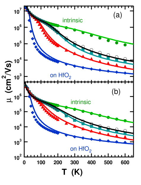
The two optical phonons at the point have couplings for LO (- sign) and TO (+ sign) modes respectively Piscanec ; Ando1 , where eV/Å Ando2 , for electrons and for holes. The K-point TO phonon mode has an electron-phonon coupling twice as large PerebeinosCNT1 ; Piscanec , with the angle dependence given by Piscanec . The effect of the optical phonons (both at and ) on the low-field mobility can be calculated according to Ferry :
| (3) |
where eV/Å is an effective electron-optical phonon coupling. The angle integration in Eq. (1) for -point phonons gives a factor of larger contribution than that for -point phonons scattering.
The SPP phonons on polar substrates produce an electric field that couples to the electrons on the nearby graphene. While the SPP scattering is of lesser importance in conventional Metal Oxide Semiconductor Field-Effect Transistors (MOSFETs)Fischetti , it is much more prominent in graphene and carbon nanotubes due to the much smaller vertical dimension of the devices given by the van der Waals distance. It has been invoked to explain transport under both low and high bias conditions in graphene Fuhrer_sio2 ; Shepard ; Gunea ; Jena and carbon nanotubes PerebeinosSPP on polar substrates. In graphene the SPP coupling is given by Gunea ; Jena :
| (4) | |||||
where Å is the van der Waals distance between the polar substrate and the graphene flake. The magnitude of the polarization field is given by the Frhlich couplingMahanSPP : , where is a surface phonon energy and and are the low- and high-frequency dielectric constants of the polar substrate, see Table 1. The screening of the Coulomb interaction by the environment above the polar dielectric is taken into account by . Since the screening of the electric field perpendicular to the graphene plane is weak Louie_eps , we take . When there are several SPP modes with an appreciable coupling, then the low- and high- frequency are understood as intermediate dielectric functions at for and at for Fischetti .
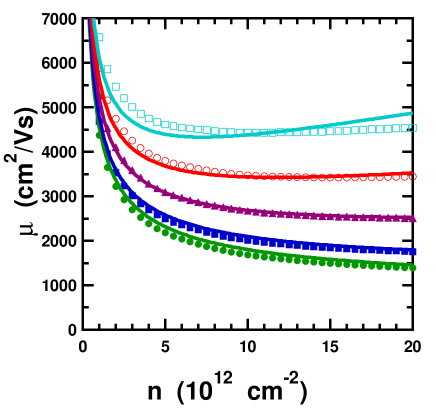
As shown in Fig. 1, the SPP contribution to the low-field mobility can be well approximated by:
| (5) |
which is a non-monotonic function of carrier density . Here , where parameters and eV are determined to give an overall agreement of the mobility dependence on the carrier density and distance , as shown in Fig. 2. SiC grown graphene has an intermediate dead layer SiCdead , which increases the effective distance and also changes the environmental screening . Both effects, have to be taken into account when direct comparison is made with the experiment. Note that the calculated temperature dependencies shown in Fig. 1 deviate from the scattering rate temperature dependence given by the SPP phonon occupation number . An additional temperature dependence arises from the thermal averaging of the scattering rate with the carrier distribution function. We have chosen a set of parameters and to agree best with the mobility at room temperature.
The calculated low-field mobility from the BTE solution in Fig. 1 can be well described using Matthiessen’s rule:
| (6) |
where mobility contributions due to the acoustic, optical, and SPP phonons are given by Eq. (2), (3), and (5), respectively.
III Current Saturation
At high bias, the transport in graphene is usually described by the saturated current model Shepard ; PerebeinosCNT1 ; Pierret :
| (7) |
where is the total carrier density, is a saturation velocity, and is an electric field. Note that in the model . Within simple model, in the full saturation regime only carriers around the Fermi energy in the energy window contribute to the current. Here is the characteristic frequency of the phonon responsible for the current saturation. The saturated velocity can then be calculated and for :
| (8) |
Note again a difference in the numerical prefactor used in the literatureShepard ; Freitag ; Barreiro versus which affects the numerical value of the characteristic phonon energy extracted from the experiments Shepard ; Freitag .
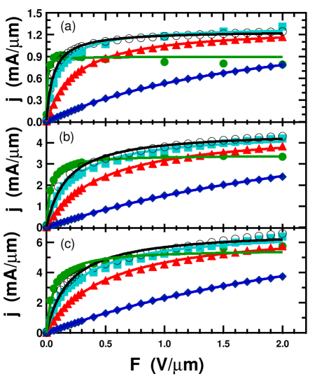
The current densities for graphene on different substrates as a function of electric field are shown in Fig. 3. When phonons are kept in thermal equilibrium at K, the current does not show full saturation for the experimentally relevant source-drain fields up to 2 V/m. In Fig. 3a, the current shows negative differential conductance for scattering by intrinsic graphene phonons. This behavior is due to the deviation of the bandstructure from the linear band dispersion, similar to the effect of the non-parabolicity in carbon nanotubes PerebeinosCNT1 . While the current at high bias in Fig. 3 is found to be larger for graphene on polar insulators with larger SPP phonon energy, the saturated velocity as obtained from the fit to Eq. (7) does not obey Eq. (8).
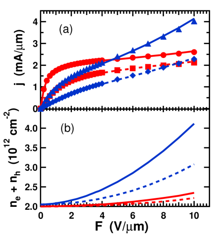
First we explore the dependence of the saturated velocity on the low-field mobility. The latter is strongly affected by the quality of the substrate, which introduces Coulomb impurity scattering Cheanov ; AndoCoulomb ; MacDonaldCoulomb ; DasSarma2 ; Fuhrer ; HwangSarmaCoul ; Fuhrer_sio2 ; Wendy , resonant scatterers Ostrovky1 ; Katsnelson2 ; Stauber , electron-hole puddles puddle , and surface roughness Katsnelson1 ; Heinz_rough . In Fig. 4a we show current-voltage characteristics of graphene on SiO2 with a variable Coulomb impurity concentration following Ref. DasSarma2 . Despite the fact that the low-field mobilities vary by a factor of , the saturated velocity, as obtained form the fit to Eq. (7), is essentially the same. The electronic temperature increases with the electric field, such that minority carriers contribution to the current becomes significant. This effect is more prounced at elevated lattice temperatures as shown in Fig. 4b.
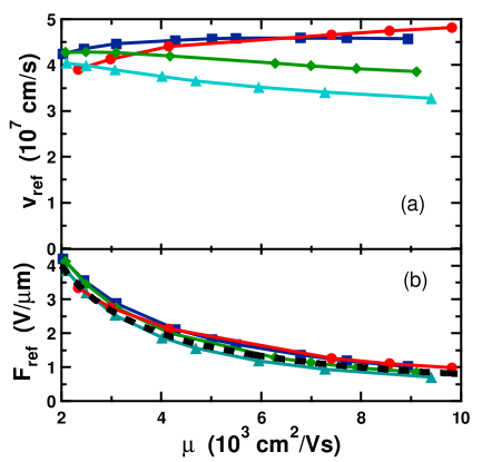
The systematic behavior of the low-field mobility, which is modified by the impurity concentration, on the saturated velocity is shown in Fig. 5. Since the current does not fully saturate even at large fields, we have chosen to plot in Fig. 5 a reference velocity calculated at the reference field where the mobility is reduced by a factor of two. If Eq. (7) is applicable, then the reference velocity is equal to half the saturated velocity and is reached at a reference field of . We find that the reference velocity is about cm/s and has little dependence on either carrier density or low-field mobility in the parameter space considered here. The reference field is inversely proportional to the low-field mobility as shown in Fig. 5b, which justifies the functional form Eq. (7) used to analyze the BTE results.
IV Self-Heating effect on current saturation
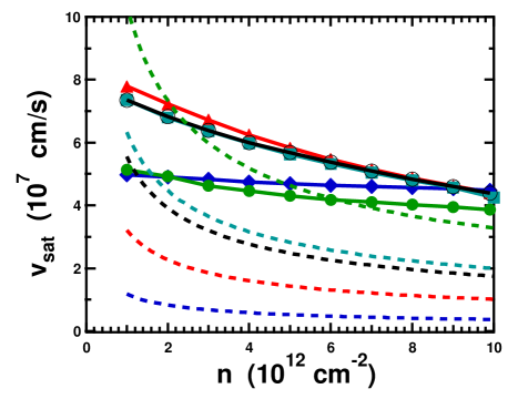
The analysis of both experimentalShepard ; Freitag ; Barreiro and simulation Guo results had often relied on Eq. (8). In Fig. 6 we show that Eq. (8) fails qualitatively to describe the results of the BTE simulations. In particular, saturated velocity in graphene on SiO2 is predicted to be very similar to that in graphene on BN and SiC substrates, although SPP phonon energies in the latter are almost a factor of two larger. While Eq. (8) predicts a variation of by more than an order of magnitude for the range of and used in Fig. 6, we find the values of from the fits to Eq. (7) to be within cm/s. The saturated velocity in intrinsic graphene shown by green curve in Fig. 6 agrees well with the Monte Carlo BTE solution in low density limit in Ref. Goldman . At the same time, the reported experimental valuesShepard ; Freitag of at densities of cm-2 are below cm/s, which is at least a factor of smaller than that in Fig. 6.
We suggest that one of the factors for the apparent discrepancy is the self-heating effect. The temperature rise was shownFreitag to be proportional to the Joule losses , where is the ambient temperature and the thermal conductance controls the heat dissipation. This simple picture applies only for graphene regions away from the contacts such that both the thermal contact resistance and the substrate thermal conductivity determine the value of . Note that the upper bound for , which corresponds to zero contact thermal resistance, is determined by the thermal conductivity and thickness of the insulating substrate. For example, thermal conductivity of SiO2 is W/(mK) CRC and for the insulator height of nm a maximum value of kW/(K cm2) is expected. However, this upper bound can be significantly reduced due to the thermal contact resistance as in Ref. Freitag .
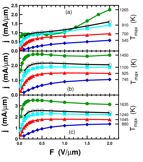
In the presence of the SPP scattering the role of the thermal contact resistance is minimized because electrons can give some of their energy directly to the substrate SPP phonons Rotkin ; MahanKapitza . In our “self-heating model” we assume that SPP and graphene phonons are heated to the same temperature, which is proportional to the Joule losses found self-consistently, i.e. . In substrates with much higher thermal conductivities, such as SiC, BN and HfO2, the thermal contact resistance would dominate the value of . In this case a full self-consistent solution including thermal transport in the substrate, which determines the SPP phonon temperature, would be needed. In Fig. 7 we find that the current densities drop by up to a factor of four at high biases as a result of self-heating for kW/(Kcm2). Moreover, the current now shows true saturation at experimental source-drain fields, which are much smaller than calculated in Fig. 5b at room temperatures, and the high bias currents are comparable to those reported in Ref. Shepard ; Freitag .
At high density, the self-heating involving the intrinsic graphene phonons is predicted here to lead to negative differential conductance. This effect has served as an experimental signature of the self-heating in suspended carbon nanotubes Dai . In the presence of SPP scattering the negative differential conductance is less pronounced and the self-heating effect leads to current saturation in Fig. 7. The different outcome of self-heating effects leading to either negative differential conductance or current saturation can well be understood by the difference in the graphene phonon and SPP phonon energies. Indeed, the current density in the diffusive regime is . According to Eq. (1), the self-heating reduces the scattering time as , such that . In the high temperature limit and current saturates as , where we have used the self-heating temperature . The saturation current in this simple picture depends on as , which is in qualitative agreement with a full BTE solution shown in Fig. 8b. On the other hand, the large intrinsic graphene optical phonon leads to an activated temperature dependence of the scattering time, which produces the negative differential conductance in Fig. 7.
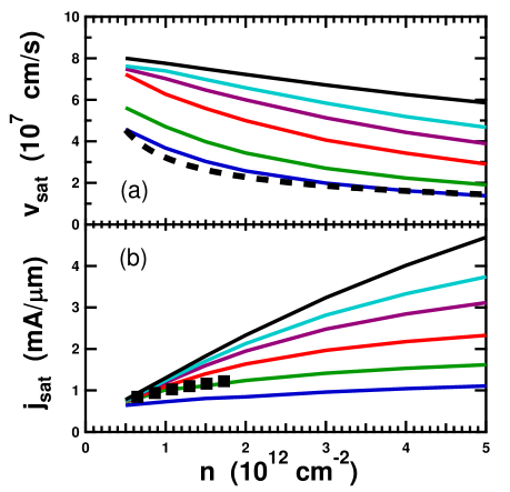
The effect of the thermal conductance on velocity saturation is explored in Fig. 8. As is reduced from infinity to 0.25 kW/(K cm2), the saturated velocity drops by a factor of four. For small values of and large densities, we find that Eq. (7) fails to fit the results of calculations in the full range of fields and we have chosen to fit a range of fields from 0.5 to 1 V/m, where saturation is almost attained. The calculated saturated current in Fig. 8b for kW/(K cm2) agrees remarkably well with recent measurements in Ref. Barreiro . The data from Ref. Barreiro are fitted to Eq. (7) as shown in Fig. 9a. Note that accidentally Eq. (8) reproduces fairly well the results of self-heating model for kW/(K cm2) in Fig. 8a.
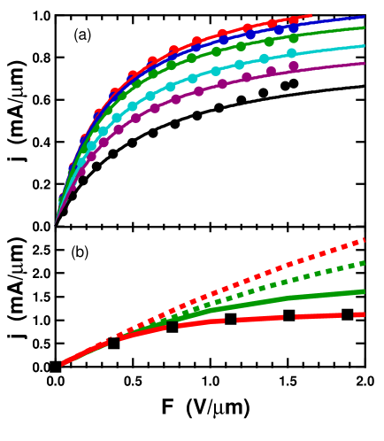
In the experiment described in Ref. Freitag , the thermal conductance was directly measured and does not have to be a fit parameter in modeling the experimental I-V curve. The observed mobility of about 1000 cm2/Vs in Ref. Freitag can be reproduced in our calculations by assuming scattering with charged impurities DasSarma2 of density cm-2 and with a smaller cm-2 in the presence of SPP scattering from the SiO2 substrate. The charge carrier density was fixed by the gate voltage at cm-2 in Ref. Freitag . In Fig. 9b we show that the calculated current is significantly larger at high biases in the presence of both intrinsic graphene and SPP phonon scattering at room temperatures. Most importantly, the current does not show the saturation that is observed in the experiment. On the other hand, using the experimentally measured temperatures, our self-heating model with kW/(K cm2) including the SPP scattering very nicely reproduces the experiment. However, if we assume self-heating model including only the graphene phonons (no SPP) we do not find full saturation, even at fields up to 2 V/m, and the calculation overestimates the measured currents at high biases.
V conclusion
In conclusion, we explored the effect of current and velocity saturation on the carrier density and impurity concentration including intrinsic graphene phonons and SPP scattering on polar substrates. The observed full current saturation is simulated only when we account for the self-heating. Without self-heating, the current densities are predicted to be too high for either graphene phonon scattering or SPP scattering. While impurity scattering modifies substantially the low-field mobility, it has little effect on the saturated velocity. Furthermore, the saturated velocity depends very weakly on carrier density and the choice of substrate. These dependencies served as the basis for invoking SPP scattering for graphene on SiO2 as the velocity saturation mechanism in Ref. Shepard ; Freitag . A more direct experimental confirmation for the SPP role in velocity saturation is desirable. We predict a factor of four enhancement of the saturation current if self-heating effects are minimized. This can be achieved by using an appropriate choice of substrate with high thermal conductivity, scaled down insulator thickness, and keeping the graphene/substrate contact thermal resistance low.
References
- (1) K.S. Novoselov, A. K. Geim, S. V. Morozov, D. Jiang, M. I. Katsnelson, I. V. Grigorieva, S. V. Dubonos, A. A. Firsov, Nature 438, 197 (2005).
- (2) Y. Zhang, J. W. Tan, H. L. Stormer, P. Kim, Nature 438, 201 (2005).
- (3) K. I. Bolotin, K. J. Sikes, Z. Jiang, D. M. Klima, G. Fudenberg, J. Hone, P. Kim, and H. L. Stormer, Solid State Commun. 146, 351 (2008).
- (4) X. Du, I. Skachko, A. Barker, and E. Y. Andrei, Nat. Nanotechnol. 3, 491 (2008).
- (5) A. H. Castro Neto, F. Guinea, N. M. R. Peres, K. S. Novoselov, and A. K. Geim, Rev. Mod. Phys. 81, 109 (2009).
- (6) A. Geim, Science 324, 1530 (2009).
- (7) Ph. Avouris, Z. Chen, V. Perebeinos, Nature Nano. 2, 605 (2007).
- (8) F. Xia, T. Mueller, Y.-M. Lin, A. Valdes-Garcia, and Ph. Avouris, Nature Nano. 4, 839 (2009).
- (9) Y.-M. Lin, K. A. Jenkins, A. Valdes-Garcia, J. P. Small, D. B. Farmer, and Ph. Avouris, Nano Lett. 9, 422 (2009).
- (10) I. Meric, N. Baklitskaya, P. Kim, K. L. Shepard, IEDM.2008.4796738 (2008).
- (11) I. Meric, M. Y. Han, A. F. Young, B. Ozyilmaz, P. Kim, K. L. Shepard, Nature Nano 3, 654 (2008).
- (12) M. Freitag, M. Steiner, Y. Martin, V. Perebeinos, Z. Chen, J. C. Tsang, and Ph. Avouris, Nano Lett. 9, 1883 (2009).
- (13) A. Barreiro, M. Lazzeri, J. Moser, F. Mauri, and A. Bachtold, Phys. Rev. Lett. 103, 076601 (2009).
- (14) R. Bistritzer and A. H. MacDonald, Phys. Rev. B 80, 085109 (2009).
- (15) J. Chauhan and J. Guo, Appl. Phys. Lett. 95, 023120 (2009).
- (16) D. H. Chae, B. Krauss, K. von Klitzing, and J. H. Smet, Nano Lett. 10 466 (2010).
- (17) W. P. Su, J. R. Schrieffer, and A. J. Heeger, Phys. Rev. Lett. 42, 1698 (1979); Phys. Rev. B 22, 2099 (1980).
- (18) S. Piscanec, M. Lazzeri, F. Mauri, A.C. Ferrari, and J. Robertson, Phys. Rev. Lett. 93, 185503 (2004); M. Lazzeri, S. Piscanec, F. Mauri, A. C. Ferrari, and J. Robertson, Phys. Rev. Lett. 95, 236802 (2005).
- (19) C.-H. Park, F. Giustino, M. L. Cohen, and S. G. Louie, Phys. Rev. Lett. 99, 086804 (2007).
- (20) M. Lazzeri, C. Attaccalite, L. Wirtz, and F. Mauri, Phys. Rev. B. 78, 081406(R) (2008).
- (21) V. Perebeinos, J. Tersoff and Ph. Avouris, Phys. Rev. Lett. 94, 086802 (2005).
- (22) We use some avaraged values from several reports Fischetti ; Gunea ; Jena .
- (23) M. V. Fischetti, D. A. Neumayer, and E. A. Cartier, J. of Appl. Phys. 90, 4587 (2001).
- (24) Properties of Silicon Carbide, edited by Gary L. Harris (INSPEC, the Institution of Electrical Engeneers, London, UK, 1995).
- (25) R. Geick, C. H. Perry, G. Rupprecht, Phys. Rev. 146, 543 (1966).
- (26) L. Pietronero, S. Strassler, H. R. Zeller, and M. J. Rice, Phys. Rev. B 22, 904 (1980).
- (27) For wavevector arbitrary away from -point, the angle is given by , where .
- (28) L. M. Woods and G. D. Mahan, Phys. Rev. B 61, 10651 (2000).
- (29) H. Suzuura and T. Ando, Phys. Rev. B 65, 235412 (2002).
- (30) V. Perebeinos and J. Tersoff, Phys. Rev. B 79, 241409(R) (2009).
- (31) E. H. Hwang and S. Das Sarma, Phys. Rev. B 77, 115449 (2008).
- (32) S. Ono and K. Sugihara, J. Phys. Soc. Jpn. 21, 861 (1966).
- (33) Ko Sugihara, Phys. Rev. B 28 2157 (1983).
- (34) K. I. Bolotin, K. J. Sikes, J. Hone, H. L. Stormer, and P. Kim, Phys. Rev. Lett. 101, 096802 (2008)
- (35) J. H. Chen, C. Jang, S. Xiao, M. Ishigami, M. S. Fuhrer, Nature Nano 3, 206 (2008).
- (36) X. Hong, A. Posadas, K. Zou, C. H. Ahn, and J. Zhu, Phys. Rev. Lett. 102, 136808 (2009).
- (37) E. H. Hwang and S. Das Sarma, Phys. Rev. B. 79, 165404 (2009).
- (38) T. Ando, J. Phys. Soc. J. 75, 124701 (2006).
- (39) K. Ishikawa and T. Ando, J. Phys. Soc. Jpn. 75, 084713 (2006); S. Piscanec, M. Lazzeri, J. Robertson, A. C. Ferrari, and F. Mauri, Phys. Rev. B 75, 035427 (2007).
- (40) R. S. Shishir and D. K. Ferry, J. Phys.: Cond. Matt. 21, 232204 (2009).
- (41) S. Fratini and F. Guinea, Phys. Rev. B 77, 195415 (2008).
- (42) A. Konar, T. Fang, and D. Jena, arXiv:0902.0819.
- (43) V. Perebeinos, S. V. Rotkin, A. G. Petrov, and Ph. Avouris, Nano Lett. 9, 312 (2009).
- (44) S. Q. Wang and G. D. Mahan, Phys. Rev. B 6, 4517 (1972).
- (45) L. X. Benedict, S. G. Louie, and M. L. Cohen, Phys. Rev. B. 52, 8541 (1995).
- (46) J. Hass, R. Feng, J. E. Millan-Otoya, X. Li, M. Sprinkle, P. N. First, W. A. de Heer, and E. H. Conrad, and C. Berger, Phys. Rev. B 75, 214109 (2007).
- (47) R. F. Pierret, Semiconductor Device Fundamentals (Addison Wesley Longman, Reading, 1996).
- (48) V. V. Cheianov and V. I. Fal ko, Phys. Rev. Lett. 97, 226801 (2006).
- (49) T. Ando, J. Phys. Soc. Jpn. 75, 074716 (2006).
- (50) K. Nomura and A. H. MacDonald, Phys. Rev. Lett. 98, 076602 (2007).
- (51) E. H. Hwang and S. Das Sarma, Phys. Rev. B 77, 195412 (2008). The environment dielectric constant is and charged impurities are assumed to be located in the graphene plane.
- (52) J. H. Chen, C. Jang, S. Adam, M. S. Fuhrer, E. D. Williams, and M. Ishigami, Nature Phys. 4, 377 (2008).
- (53) W. Zhu, V. Perebeinos, M. Freitag, and Ph. Avouris, Phys. Rev. B 80, 235402 (2009).
- (54) P. M. Ostrovsky, I. V. Gornyi, and A. D. Mirlin, Phys. Rev. B 74, 235443 (2006).
- (55) M. I. Katsnelson and K. S. Novoselov, Solid State Commun. 143, 3 (2007).
- (56) T. Stauber, N. M. R. Peres, and F. Guinea, Phys. Rev. B 76, 205423 (2007).
- (57) J. Martin , N. Akerman , G. Ulbricht , T. Lohmann , J. H. Smet , K. von Klitzing , and A. Yacoby, Nature Phys. 4, 144 (2008).
- (58) M. I. Katsnelson and A. K. Geim, Phil. Trans. R. Soc. A 366, 195 (2008).
- (59) C. H. Lui, L. Liu, K. F. Mak, G. W. Flynn, and T. F. Heinz, Nature 462, 339 (2009).
- (60) A. Akturk and N. Goldsman, J. of Appl. Phys. 103, 053702 (2008).
- (61) Materials Science and Engineering Handbook edited by James F. Shackelford, William Alexande, (CRC Press LLC, Boca Raton, 2000)
- (62) S. V. Rotkin, V. Perebeinos, A. G. Petrov, and Ph. Avouris, Nano Lett. 9, 1850 (2009).
- (63) G. D. Mahan, Phys. Rev. B 79, 075408 (2009) and references therein.
- (64) E. Pop, D. Mann, J. Cao, Q. Wang, K. E. Goodson, and H. J. Dai, Phys. Rev. Lett. 95, 155505 (2005).