Gating of high-mobility two-dimensional electron gases in GaAs/AlGaAs heterostructures.
Abstract
We investigate high-mobility two-dimensional electron gases in heterostructures by employing Schottky-gate-dependent measurements of the samples’ electron density and mobility. Surprisingly, we find that two different sample configurations can be set in situ with mobilities differing by a factor of more than two in a wide range of densities. This observation is discussed in view of charge redistributions between the doping layers and is relevant for the design of future gateable high-mobility electron gases.
pacs:
72.20.-i, 73.23.-b, 73.40.-c, 73.63.-b1 Introduction
Two-dimensional electron gases (2DEGs) in heterostructures can reach mobilities exceeding at low temperatures, facilitating the observation of fascinating phenomena like the microwave-induced zero-resistance states, the quantum Hall state, and interactions between composite fermions [1]. It turns out that to this end, clean materials and growth techniques beyond the standard modulation doping approach are essential [2, 3, 4]. However, current growth protocols are apparently in conflict with the in situ control of the 2DEG’s density via Schottky-gates: recent experiments on gated high-mobility structures have reported hysteresis effects and temporal drifts when biasing Schottky gates [5, 6]. In order to investigate the origin of these effects, we fabricate gated Hall bars containing a high-mobility 2DEG.
2 Experiment
In the investigated samples, the 2DEG resides in a wide GaAs quantum well, beneath the surface. The overall growth scheme is similar as previously reported [8]. Two Si-donor layers are situated at depths of about and in order to compensate for surface-states and background impurities in the substrate. Since these donors are embedded in , they are expected to form DX-centers below the -band [7]. Layers of GaAs at and are -Si doped and enclosed by thick layers of AlAs. The ground state in the AlAs wells (-minima) is lower than that in the GaAs wells ( minima). Consequently, only a part of the donors’ free electrons reside in the high-mobility 2DEG, whereas the rest is expected to populate the -band within the AlAs-layers embedding the doping planes [2, 8].
The investigated samples stem from different wafers with the same layer structure. Typical transport characteristics of unprocessed samples are a Drude mobility at an electron density as measured in van-der-Pauw geometry at a temperature of (data not shown).
The samples are etched deep to define a wide Hall bar. AuGe pads are deposited and annealed to contact the 2DEG. In a final step, of Ti/Au are deposited on the Hall bar to form a Schottky top-gate.
Figure 1 (a) shows the uppermost of the heterostructure’s conduction band edge, calculated self-consistently for different top gate voltages 111We employ the 3D nanodevice simulator , available at http://www.nextnano.de. The electrochemical potential (defined as ) is assumed to be pinned mid-gap in the substrate and below the conduction band at the surface. For the sake of simplicity, dynamic processes are not taken into account and the ionisation degree of the DX-dopants dopants is assumed to be independent of gate voltage. The doping concentrations at and have been chosen so that both the 2DEG’s electron density at and the pinch-off voltage are consistent with the experimentally determined values. The chosen value of is smaller than the density of silicon atoms of , suggesting that only part of the donors are electrically active.
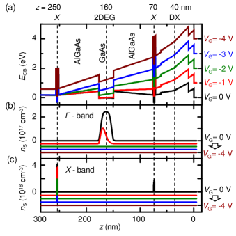
The gate is situated at the surface () and is set to , respectively (black, red, green, blue and maroon trace). Figure 1 (b) shows the calculated free electron density in the -band for these gate voltages. Applying reduces the 2DEG’s electron density and shifts the wave function to the lower boundary of the well (red trace). The 2DEG is depleted when applying (green trace). Figure 1 (c) shows the electron density in the -band for the same set of gate voltages. At (black trace), electrons occupy the AlAs layers at and with the respective electron densities in the -band being (upper layer) and (lower layer). Applying (red) depletes the upper layer of -electrons and depletes also the bottom layer of -electrons.
The samples’ transport properties are measured at low temperatures employing a standard lock-in technique with a typical modulation frequency of and an amplitude . The Hall density is obtained from the measured source-drain current and the transversal four terminal voltage via the relationship . Here, is the magnetic field strength applied perpendicular to the plane of the 2DEG and denotes the elementary charge. Starting from positive gate bias , the gate voltage is swept with a rate of to and back to . The upper limit of is determined by the onset of leakage current, whereas the lower boundary of was empirically chosen because larger voltage loops do not change the results described in the following. The calculated electron densities shown in figure 1 (c) suggest that this lower border is correlated with the depletion of the lower layer of -electrons for .
Figure 2 (a) shows the measured electron density as a function of the gate bias in magnetic field oriented perpendicular to the plane of the 2DEG.
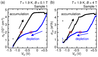
Clearly, there is a strong hysteresis between depletion (blue trace) and accumulation of the 2DEG (black). For comparison, two red circles highlight the gate voltages where . Figure 2 (b) shows a similar measurement repeated at , where the density is expressed as the transversal magnetoconductance in units of . Having entered the quantum Hall regime, plateaus of correspond to integer filling factors and hence . Again, gate voltages corresponding to the electron density are marked by red circles. These voltages match the values from Figure 2 (a), implying that the classical Hall density matches the quantum Hall density and no populated second subband or other parallel conducting channels contribute to the measured electron densities within experimental accuracy, as confirmed by zero resistance minima in Shubnikov-de-Haas data (not shown). For both measurements, as long as the 2DEG density is being reduced, is not linear with respect to the gate bias. In contrast, the electron density increases linearly with a slope of while accumulating the 2DEG, being in good agreement with the model of a parallel-plate capacitor defined by the gate and the 2DEG 222Assuming the plates to be formed by the top gate and the 2DEG at a depth of , the expected slope is given by , where is the capacity between top gate and 2DEG, the dielectric constant of and is the electric field constant.. This qualitative difference indicates that charge redistributes in the region between gate and 2DEG during depletion but not during accumulation of the 2DEG.
Figure 3 (a) shows the electron density of another sample with the same heterostructure layer sequence, measured at and temperature .
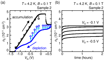
Again, the electron density shows a strong hysteresis between depletion (blue) and accumulation (black) of the 2DEG. Interrupting the gate-sweep during depletion and waiting for two hours results in an increased electron density (blue circles). In contrast, the same procedure during accumulation shows that the electron density is stable for at least one hour during accumulation (black circles). The finding implies that the charge redistribution is complete at gate biases and is stable in time afterwards. As a comparison, the temporal evolution of the electron density during depletion is shown in figure 3 (b). Stopping the gate-sweep at one of the gate voltages results in a slow recovery of the electron density.
A probable origin of the observed charge redistributions is the charging of the layer beneath the surface and/or the -electrons at . Thus, the observed hysteresis resembles the memory-like behaviour in 2DEG samples with vertically tunnel coupled self-assembled quantum dots [9, 10]. The layers would build up positive charge during depletion up to full ionisation at very negative gate voltages . According to the calculation of the band structure in figure 1 (a), electrons would not be able to repopulate the layers unless a sufficiently positive gate bias is applied. In the gate-sweeps in figures 2 and 3, such a reset of the 2DEG’s density is indeed observed when ramping the gate voltage up to . The more drastic reset at (figure 3) indicates that the time constant of the associated charge redistribution is temperature dependent.
Different charge configurations of the doping layers are expected to have a strong impact on the Drude mobility of the 2DEG, where is the longitudinal potential drop and is the aspect ratio of the Hall bar. Figure 4 shows the mobility, plotted as a function of the electron density at , during a gate-sweep from to and back to .
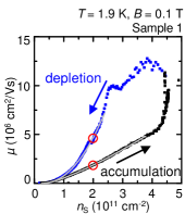
While depleting, the mobility is clearly larger than during accumulation at any given density (e.g., as compared to at , red circles). When accumulating, a recovery of the mobility sets in at electron densities , corresponding to gate voltages .
For temperatures of , we find that the mobility is independent of temperature (measurement not shown), indicating that phonon scattering is not relevant for the interpretation of this gate-sweep. The fit of a power-law dependence to the data yields exponents of (depleting) and (accumulating) 333The other fitting parameters are , during depletion and , during accumulation. Such dependence is commonly associated with remote impurity scattering of ionised donor atoms [11] and is in contrast to found in background-impurity-limited 2DEGs [3].
From the strong positive -dependence of our sample’s mobility it can be concluded that the dominant scatterers are characterized by a potential whose Fourier transform diminishes strongly when is increased. The significantly larger exponent and the higher mobility during depletion suggest that during depletion, the disorder potential is steeper in -space, corresponding to a smoother (long-range-)potential in real space.
The observed decrease of the mobility with decreasing electron density could be caused by several effects:
-
1.
Decreasing the electron density increases the Fermi-wavelength. This in turn facilitates scattering events that arise from the long-range part of the disorder potential [12].
-
2.
-electrons, which screen the dopants’ disorder potential at , are depleted at sufficiently negative gate bias. The loss of the screening layer might have a strong impact on the 2DEG’s mobility.
-
3.
During depletion, dopants between gate and 2DEG become ionised which leads to increased remote ionised impurity scattering.
-
4.
At more negative gate biases (and hence lower densities), the confinement potential of the 2DEG is more strongly tilted. In this situation, the weight of the 2DEG’s wave function is situated closer to the lower AlGaAs-barrier, increasing alloy scattering and interface roughness scattering [13].
The observation of different mobilities at the same density can not be related to the first effect, because the Fermi wavelength is the same in both cases. In order to test the impact of ionised donors above the 2DEG onto the mobility, the temporal evolution of the mobility is shown in Figure 5.
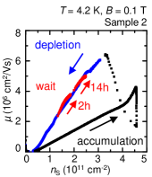
The mobility is measured at a temperature of (compared to in Figure 4) in order to speed up the relatively slow process of ionisation. As a consequence, the dependence of the mobility on the density is almost linear due to enhanced phonon scattering [11], but still the mobility is higher during depletion than during accumulation. During depletion (blue), the gate-sweep is stopped and the change of the sample’s density and mobility are recorded. Starting from (lower red trace) or (upper red trace), both the density and mobility increase over time. The evolution follows the depletion curve, indicating that the progressing ionisation acts primarily as a positive gate bias and does not determine the mobility at a given electron density. This leads us to believe that the drastic change of the mobility after fully depleting the 2DEG is not due to changes of the charge states of the screening layer at or the doping layer at , but rather due to the screening layer at . After depleting both the 2DEG and this lower screening layer, more positive charge is present beneath the 2DEG, increasing interface roughness scattering and alloy scattering due to a more tilted confinement potential. Additionally, the loss of this screening layer should increase the 2DEG’s remote ionised impurity scattering with dopants beneath the 2DEG. The latter effect might be weaker than the effect of a tilted potential, because the mobility shown in figure 4 does not show a drastic decrease at the gate voltage corresponding to the expected depletion of the upper screening layer.
The finding implies that the bottom screening layer cannot be refilled laterally (from non-depleted areas of the Hall bar) but requires vertical tunnelling or an additional activation energy to regain its’ original -electron density. In order to test this interpretation, the response of the electron density to illumination with an infrared light emitting diode (IR-LED) is investigated. According to the bandstructure calculation shown in figure 1 (a), the conduction band edge of the doping layers between top gate and 2DEG is above the Fermi energy for gate voltages . Hence, we expect an increase of the electron density in the 2DEG if the LED affects these doping layers by facilitating further ionisation. In contrast, the band edge of the screening layer at is situated below the Fermi energy as long as the 2DEG is populated. If the LED resets the positively charged bottom screening layer, the electron density of the 2DEG should decrease. Figure 6 shows the electron density at , , plotted as a function of gate voltage.
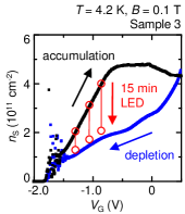
Sweeping the gate bias from to (blue curve) and back to (black) creates again a strong density hysteresis. When the gate-sweep is stopped during accumulation and the IR-LED is switched on by applying a current of , the density decreases over time, implying that indeed a repopulation of the screening layer at is observed. Vertical red lines at voltages show that the density decreases almost towards the depletion value during of illumination, rather than approaching the value after waiting (see figure 3). This suggests that some photo-generated electrons get trapped in the upper screening layer. Indeed, once the LED is switched off, a slow increase of the electron density is observed (data not shown), being consistent with the time dependencies shown in figure 3.
3 Conclusion
In conclusion, we investigated gating effects in high-mobility 2DEGs. It is found that a gate-induced ionisation of the doping layers between top-gate and 2DEG causes a significant hysteresis in the electron density. Surprisingly, this ionisation has almost no impact on the 2DEG’s mobility at a given electron density. On the other hand, the depletion of the screening layer beneath the 2DEG is found to decrease the mobility by more than a factor of 2. This drastic effect can be explained by a reduced screening of dopants and a shift of the 2DEG’s wave function towards its’ lower AlGaAs boundary. Our finding indicates that for gatable high-mobility 2DEGs, it is important to keep the 2DEG wave function in the center of the quantum well which could for example be achieved through a buried back gate. At the same time any possible screening from X-electrons needs to be (and can be) sacrificed in order to achieve large density tunability.
References
References
- [1] Pfeiffer L and West K W 2003 Physica E 20 57
- [2] Friedland K-J, Hey R, Kostial H, Klann R and Ploog K 1996 Phys. Rev. Lett. 77 4616
- [3] Umansky V, de Picciotto R and Heiblum M 1997 Appl. Phys. Lett. 71 683
- [4] Hwang E H and Sarma S D 2008 Phys. Rev. B. 77 235437
- [5] Dolev M, Heiblum M, Umansky V, Stern A and Mahalu D 2008 Nature 452 829
- [6] Miller J B, Radu I P, Zumbühl D M, Levenson-Falk E M, Kastner M A, Marcus C M, Pfeiffer L N and West K W 2007 Nature Physics 3 561
- [7] Mooney P M 1990 J. Appl. Phys. 67
- [8] Umansky V, Heiblum M, Levinson Y, Smet J, Nübler J and Dolev M 2009 Journal of Crystal Growth 311 1658
- [9] Kannan E S, Kim Gil-Ho, Farrer I and Ritchie D A 2007 J. Phys.: Condens. Matter 19 506207
- [10] Marquardt B, Geller M, Lorke A, Reuter D and Wieck A D, 2009 Appl. Phys. Lett. 95 022113
- [11] Hirakawa K and Sakaki H 1986 Phys. Rev. B. 33 8291
- [12] Ando T, Fowler A B and Stern F 1982 Rev. Mod. Phys. 54
- [13] Bockelmann U, Abstreiter G, Weimann G and Schlapp W 1990 Phys. Rev. B. 41 7864