Origin of half-semimetallicity induced at interfaces of C-BN heterostructures
Abstract
First-principles density functional calculations are performed in C-BN heterojunctions. It is shown that the magnetism of the edge states in zigzag shaped graphene strips and polarity effects in BN strips team up to give a spin asymmetric screening that induces half-semimetallicity at the interface, with a gap of at least a few tenths of eV for one spin orientation and a tiny gap of hundredths of eV for the other. The dependence with ribbon widths is discussed, showing that a range of ribbon widths is required to obtain half-semimetallicity. These results open new routes for tuning electronic properties at nanointerfaces and exploring new physical effects similar to those observed at oxide interfaces, in lower dimensions.
pacs:
73.20.-r, 73.22.Pr, 75.70.CnI
A number of new physical phenomena have been discovered in the last few years at the interfaces between very different materials. The electronic reconstruction induced at these boundaries can give rise to metallic statesOhtomo and Hwang (2004), magnetismBrinkman et al. (2007), or even superconductivityReyren et al. (2007), although the parent compounds were originally insulating oxides. But not only boundaries of bulk materials are important: in two dimensional graphene nanoribbons (GNR) edges have become relevant, with peculiar electronic states localized at the boundary of the ribbonsFujita et al. (1996).
Since its first experimental realizationNovoselov et al. (2004), graphene has emerged as a prominent candidate to replace silicon in the development of high performance electronic devices. However, the extremely high mobility of charge carriers in graphene (ten times higher than that in silicon wafers used in microprocessors) poses a difficulty for the fabrication of nanodevices based on this material. A possible route to harness the conducting charges in graphene transistors is the fabrication of graphene nanoribbons, where the lateral confinement of charge induces the opening of a gap that depends on the orientation of the GNR, and is inversely proportional to its widthHan et al. (2007); Son et al. (2006a). Interestingly, ribbons with zigzag shaped border (ZGNR) present a local ferrimagnetic structure at the edgeFujita et al. (1996), and upon application of an in-plane external electric field can be tuned into a half-metallic state, with a gap opening for one spin component, and a metallic behavior for the other, hence giving a full spin polarization of the conducting electronsSon et al. (2006b). Theoretical calculations have shown that similar magnetic edge states exist in zigzag edged BN nanoribbons (ZBNNR)Barone and Peralta (2008); Zheng et al. (2008). The recent experimental realization of BN nanosheetsPacilé et al. (2008); Jin et al. (2009), opens new prospects for the combination of these two isostructural materials. Hence, a proper characterization of these hypothetical semimetal-insulator junctions is much needed.
Different C/BN heterostructures have been proposed in the past, and substantial efforts have been devoted to the growth of composite sheets and nanotubesKawaguchi (1997). Laser vaporization grown C-BN single walled nanotubes show traces of the patterning of segregated BN nanodomains embedded in the carbon network sequentially along the tube axisEnouz et al. (2007). Recently, Du et. al. used first principles Molecular Dynamics calculations to prove that hybrid C-BN nanotubes can be spontaneously formed via the connection of BNNR and GNR at room temperatureDu et al. (2009), and Ding et. al. investigated the stability of C doped BNNR, showing that, under suitable conditions, GNR can be grown embedded in BN sheetsDing et al. (2009). Furthermore, it is reported that half-metallicity originates for sufficiently wide ZGNRsDing et al. (2009). Tuning half-metallicity by edge modification in ZGNR and ZBNNR has been demonstrated by othersZheng et al. (2008); Kan et al. (2008); Dutta et al. (2009); Wu et al. (2009), and understood in terms of a potential difference between the two edges through chemical modification with electron accepting or donating groups. If this was the explanation for the half-metallicity in GNR embedded in BNNR, then there should be half-metallicity independently of the BNNR width. This doesn’t seem to be the case, as the results in reference Dutta et al., 2009 suggest that there is a critical thickness for the BNNR to induce half-metallicity in GNRs.
Here, I argue that the electronic properties of C+BN heterostructures can be described in terms of the 1D equivalence of bidimensional oxide heterojunctions made of a metal (semimetal graphene) and an insulator (BN sheet). In particular, it will be shown that the polarity discontinuity in BN nanoribbon and the screening by the mobile electrons in graphene are behind the electronic reconstruction at the interface. Hence, a dependence with the BNNR width (polarity) and GNR width (number of available screening carriers) is expected.
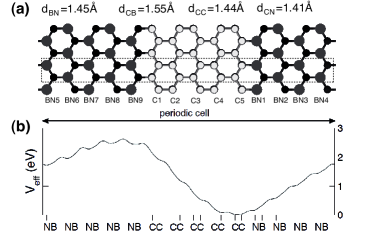
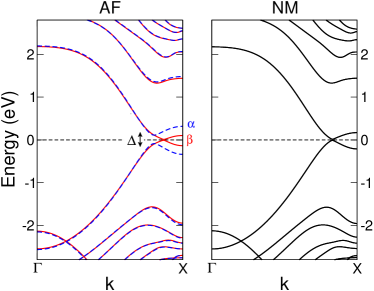
Ab initio pseudopotential density functional calculations are performed in zigzag edged Graphene-BN superlattices, within the spin-polarized generalized-gradient approximation as implemented in the SIESTA methodSoler et al. (2002). Troullier-Martin type pseudopotentialsTroullier and Martins (1991) and numerical atomic orbitals with double- plus polarization are used to describe the electronic valence states. The atomic positions are determined with a structural relaxation until the forces are smaller than 0.02eV/Å. A total of 67 k-points are used to sample the Brillouin zone. Following the conventional nomenclature -ZGNR and -ZBNNR combine to give a -superlattice with zigzag chains of graphene and zigzag chains of BN (Fig. 1a). A set of systems with and are considered, with superlattice’s periodicities in the range 1.7-4.7nm. The smaller systems () show non-magnetic (NM) semiconducting properties, with a direct energy gap that decreases with the increase in the width of the graphene ribbon. For wider systems however the gap is reduced and the system semimetallic, with edge states that give rise to a narrow band near the Fermi level, enabling the possibility of magnetic orderings induced by the electron-electron interactionFujita et al. (1996). Indeed, spin-polarized edge states are obtained in the calculations, that correspond to antiferromagnetic (AF) alignments of the spin moments at opposite edges of the heterostructure (Fig. 2), with the AF state being a few meV lower than NM, in agreement with calculations of magnetic edge states in isolated ZGNR, and ZGNR embedded in ZBNNRDing et al. (2009). Double periodicity unit cells were used to explore other magnetic orderings observed for isolated BNNRBarone and Peralta (2008), but the AF-phase remained as the ground state. Notice that hybrid exchange-DFT functionals predict a further stabilization of the AF alignment in isolated ZGNR Pisani et al. (2007). Notice also the half-semimetallic character of the AF state in Fig. 2, with an apparent gap for spin, and two bands that seem to cross the Fermi level for spin. The crossing is not allowed by symmetry because each sublattice of C atoms is linked either to B or N, breaking the sublattice’s equivalency and giving a tiny gap also for the -spin bands. Hence, the term half-semimetal is more appropriate than half-metal commonly used in the literature.


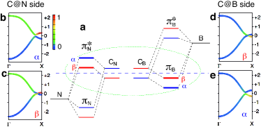
The nature of these edge bands near the Brillouin zone boundary (X-point at k=) deserves further clarification. Hydrogen passivated zigzag GNRs have insulating magnetic edge states with parallel ordering at each edge, and antiparallel alignment between the two edges. On the other hand, zigzag BNNRs have insulating, non-magnetic edge states with unoccupied state localized at the B site and occupied valence state localized at the N side. These states can be dramatically affected by edge passivationLee and Cho (2009); Zheng et al. (2008). When GNR and BNNR are attached the mixing of orbitals of C, B and N at each edge gives rise to four sets of bands that correspond to the bonding and antibonding states between C-N and C-B (Fig. 3a). The relevant bands, close to the Fermi level, are the occupied bonding C-B (), and unoccupied antibonding C-N (), each of them being a localized state at carbon atoms close to the B or N edge, respectively. Figure 3.b-e presents evidences of the highly localized states at X by showing a color contour plots for the energy bands near the Fermi level projected on the C atomic orbitals at the atoms close to the N and B edges. The localization gradually decreases as we depart from the X-point. The bonding C-N and antibonding C-B lay 5eV below and above the Fermi level respectively. Ab initio calculations have shown that the bandgaps in both C and BN zigzag nanoribbons are inversely proportional to their width, and consequently the energy separation between and in C-BN superlattices will depend on the width of each strip. Hence, a dependence of the half-semimetallic gap on the widths of the strips is anticipated, and will be discussed later.

The different electronegativities of B and N make bare ZBNNR the two-dimensional equivalent to a polar slab, with a type 3 termination, where alternating charges are ordered perpendicularly to the edge, as opposed to armchair BNNR which have type 1 boundaries and alternating charges parallel to the interfaceTasker (1979). Polarization lowers the potential felt by electrons at the nitrogen edge relative to the boron edge. Charge redistributions near the interface partially compensate this edge instability, particularly for wider ribbons, where the number of electrons that can participate in the screening is higherPark and Louie (2008). Atomic relaxations also contribute to the screening, with bonds becoming shorter at the N-side and longer at the B-side. It is then expected that mobile electrons coming from semimetallic graphene in contact with these ZBNNR will increase the screening. But this also means that there is a charge asymmetry in the GNR in contact with BN with the interface C-N being lower in energy than the C-B interface, and hence inducing a charge transfer to the N side. This charge transfer is confirmed by Mulliken population analysis, with a slightly larger charge for C atoms close to the N interface, than for C atoms close to the B edge. This result is at odds with the hypothesis that the origin of the half-metallicity in the GNR is the charge transfer from the carbon to boron atomsDutta et al. (2009). Although the occupied states close to the Fermi level are mainly localized at the atoms close to this side (Fig. 3), the fact that for very narrow ZGNR half-semimetallicity is not observedDing et al. (2009) proves that this postulate is incorrect.
The situation very much resembles that of a GNR under the presence of a transverse electric field, except that the nature of the edge states is different, with occupied bands near the Fermi level localized at the same edge (B-side) for both spin polarizations. Figure 1b shows the macroscopic averageBaldereschi et al. (1988) of the electronic effective potential in the plane of the (5,9)-superlattice. This potential profile shows a drop of 2.3eV between B and N edges, inducing an effective electric field of 0.27V/Å, which is at the brink of the critical electric field needed to induce half-metallicity in the isolated ZGNRSon et al. (2006b). The potential drop increases slightly with the BN widths studied here but the decrease of the effective polarization charge density ensures that it will saturate for sheets wide enough. For wider graphene strips, the screening is asymmetric and mainly localized a few (4 or 5) zigzag chains from the B-edge, so that the effective electric field inside the graphene ribbon will be substantially screened far from this edge. This means that the widths of the GNR and BNNR strips can be used to tune the electronic and magnetic properties of these systems.
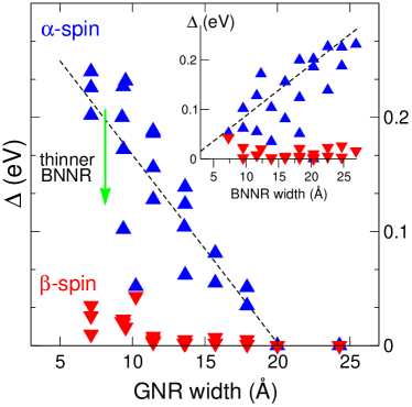
The most important result of this work is shown in Fig. 4 where the band gaps for and spins are plotted as a function of the strip widths. In the limit of broad GNR, the semimetallic behavior is recovered, with zero gap for both spins. If the GNR is too thin, the AF state is unstable and the systems becomes NM and insulating. However, lattices with sufficiently wide BN strips () and sufficiently narrow C ribbons () can show half-semimetallic properties with a gap for -spin states significantly larger (above 0.1eV) than for -spin (below 0.03eV). It is important to notice that the origin of this effect is not simply the chemical modification of the ZGNR by B or N doping, as the spin polarization disappears for narrow BN strips (inset in Fig. 4).

As mentioned before, hybrid C-BN nanotubes have already been synthesized experimentallyEnouz et al. (2007), and predictions have been made for the spontaneous formation of single-walled armchair nanotubes from the hybrid connection of BNNR and GNRDu et al. (2009). Unzipping these hybrid nanotubes would be a route to fabricate C-BN superlattices as the ones reported in this work. However, it can be shown that even in the tubular geometry the electronic and magnetic properties described above can be obtained, as long as there is a zigzag edge and the widths of BN and C ribbons are conveniently tuned, following the gap width-dependence sketched in Fig. 4. Curvature does not play an essential role, and zigzag nanotubes with can show these half-metallic properties. Details will be presented elsewherePruneda .
In addition to the demonstration that unconventional interfacial effects are not limited only to planar junctions in epitaxial complex oxides heterostructures but are present in lower dimensions, synthesis of these C-BN nanostructure offers an interesting avenue for the design of carbon-based nanospintronic devices. A zigzag-edged nanostriction of C-BN in a graphene ribbon, for example, would open a gap and induce a high spin-polarization for the transmitted electrons without the need for applied external electric fields, paving the way to efficient spin-injection in carbon structures. Surely different combination of materials can be conceived to fabricate bidimensional heterostructures and take advantage of these unusual physical phenomena that result from the combination of spin-polarized edge states and polarization induced charge dipoles at the edges. Further work on growing bidimensional superlattices that combine the exiting possibilities of nanosheets is encouraged.
Acknowledgements.
This work was supported by the CSIC through a JAE-Doc fellowship and P.I.E. 200960I025. Computational resources from the Theory and Simulation group are acknowledged. The author is thankful to P. Ordejón, E. Artacho and E. Canadell for fruitful discussions and comments.References
- Ohtomo and Hwang (2004) A. Ohtomo and H. Y. Hwang, Nature 427, 423 (2004).
- Brinkman et al. (2007) A. Brinkman, M. Huijben, M. van Zalk, J. Huijben, U. Zeitler, J. C. Maan, W. G. van der Wiel, G. Rinjders, D. H. A. Blank, and J. Hilgenkamp, Nat. Materials 6, 493 (2007).
- Reyren et al. (2007) N. Reyren, S. Thiel, A. D. Caviglia, L. F. Kourkoutis, G. Hammerl, C. Richter, C. W. Schneider, T. Kopp, A.-S. Ruetschi, D. Jaccard, et al., Science 317, 1196 (2007).
- Fujita et al. (1996) M. Fujita, K. Wakabayashi, K. Nakada, and K. J. Kusakabe, J. Phys. Soc. Jpn. 65, 1920 (1996).
- Novoselov et al. (2004) K. S. Novoselov, A. K. Geim, S. V. Morozov, D. Jiang, Y. Zhang, S. V. Dubonos, I. V. Grigorieva, and A. A. Firsov, Science 306, 666 (2004).
- Han et al. (2007) M. Y. Han, B.Özyilmaz, Y. Zhang, and P. Kim, Phys. Rev. Lett. 98, 206805 (2007).
- Son et al. (2006a) Y.-W. Son, M. L. Cohen, and S. G. Louie, Phys. Rev. Lett. 97, 216803 (2006a).
- Son et al. (2006b) Y.-W. Son, M. L. Cohen, and S. G. Louie, Nature 444, 347 (2006b).
- Barone and Peralta (2008) V. Barone and J. E. Peralta, Nano Letters 8, 2210 (2008).
- Zheng et al. (2008) F. Zheng, G. Zhou, Z. Liu, J. Wu, W. Duan, B.-L. Gu, and S. B. Zhang, Phys. Rev. B 78, 205415 (2008).
- Pacilé et al. (2008) D. Pacilé, J. C. Meyer, ¸C. Ö. Girit, and A. Zettl, Appl. Phys. Lett. 92, 133107 (2008).
- Jin et al. (2009) C. Jin, F. Lin, K. Suenaga, and S. Iijima, Phys. Rev. Lett. 102, 195505 (2009).
- Kawaguchi (1997) M. Kawaguchi, Adv. Mater. 9, 615 (1997).
- Enouz et al. (2007) S. Enouz, O. Stéphan, J.-L. Colliex, and A. Loiseau, Nano Letters 7, 1856 (2007).
- Du et al. (2009) A. Du, Y. Chen, Z. Zhu, G. Lu, and S. C. Smith, J. Am. Chem. Soc. 131, 1682 (2009).
- Ding et al. (2009) Y. Ding, Y. Wang, and J. Ni, Appl. Phys. Lett. 95, 123105 (2009).
- Kan et al. (2008) E.-J. Kan, Z. Li, J. Yang, and J. G. Hou, J. Am. Chem. Soc. 130, 4224 (2008).
- Dutta et al. (2009) S. Dutta, A. K. Manna, and S. K. Pati, Phys. Rev. Lett. 102, 096601 (2009).
- Wu et al. (2009) M. Wu, X. Wu, Y. Gao, and X. C. Zeng, Appl. Phys. Lett. 94, 223111 (2009).
- Soler et al. (2002) J. M. Soler, E. Artacho, J. D. Gale, A. García, J. Junquera, P. Ordejón, and D. Sánchez-Portal, J. Phys.: Condens. Matter 14, 2745 (2002).
- Troullier and Martins (1991) N. Troullier and J. L. Martins, Phys. Rev. B 43, 1993 (1991).
- Pisani et al. (2007) L. Pisani, J. A. Chan, B. Montanari, and N. M. Harrison, Phys. Rev. B 75, 064418 (2007).
- Lee and Cho (2009) G. Lee and K. Cho, Phys. Rev. B 79, 165440 (2009).
- Tasker (1979) P. W. Tasker, J. Phys. C: Solid State Phys. 12, 4977 (1979).
- Park and Louie (2008) C.-H. Park and S. G. Louie, Nano Letters 8, 2200 (2008).
- Baldereschi et al. (1988) A. Baldereschi, S. Baroni, and R. Resta, Phys. Rev. Lett. 61, 734 (1988).
- (27) J. M. Pruneda, to be published.