Controlling the conductance of molecular wires by defect engineering: a divide et impera approach
Abstract
Understanding of charge transport mechanisms in nanoscale structures is essential for the development of molecular electronic devices. Charge transport through 1D molecular systems connected between two contacts is influenced by several parameters such as the electronic structure of the molecule and the presence of disorder and defects. In this work, we have modeled 1D molecular wires connected between electrodes and systematically investigated the influence of both soliton formation and the presence of defects on properties such as the conductance and the density of states. Our numerical calculations have shown that the transport properties are highly sensitive to the position of both solitons and defects. Interestingly, the introduction of a single defect in the molecular wire which divides it into two fragments both consisting of an odd number of sites creates a new conduction channel in the center of the band gap resulting in higher zero-bias conductance than for defect free systems. This phenomenon suggests alternative routes toward engineering molecular wires with enhanced conductance.
I Introduction
The investigation of quantum transport through molecular systems has become an important research field in the last few decades.1Gio-Book05 Progress in measuring and fabrication techniquesAgrait has led to the continuous miniaturization of electronic devices, which have reached the point where quantum effects are important. For example, semiconductor devices have been reduced in size to the nanoscaleHisamoto00 ; Pai-Chun06 and even to the atomic scale.Huang02 ; Singh06 In addition to the report of metal atomic wires,Takayanagi ; Yanson ; Smit ; Bettini ; Ho-Chain stable and rigid carbon atomic chains have been reported recently.Cchain ; Chuvlin A key idea behind the advances in the understanding of charge transport through molecular systems is based on the view proposed by Landauer, conductance is transmission.Landauer ; Buttiker
Potential applications of molecular devices range from novel computer architecturesEllenbogen ; Joachim to chemical sensorsCui01 and medical diagnostics Patolsky04 . Among the various molecular devices, 1D conductors such as molecular wires,Moleuclar-wire ; Israel-STM ; NDLang have been considered to be one of the most fundamental components for nanotechnology. Due to the reduction of size and dimensions of materials, 1D systems show sensitive response to external field or intrisic characteristics, which can be exploited for the development of molecular devices such as biological sensorsCui01 with high sensitivity.
Polymers are one of the most promising materials for acting as 1D conductors. Their applicabilityUbiquitous ranges from displaysPPV ; OLED ; Jenekhe to thin film transistors,TFT photovoltaics,Graetzel and solar cells.Gunes ; Blom The compatibility of polymer materials with light-weight, mechanically flexible plastic substrates and new fabrication methods make them possible candidates for future electronic devices.
Intrinsic properties of molecules as well as external perturbations can strongly affect the transport properties of the resulting low dimensional devices. For example, the conductance of 1D polymers drastically depends on the concentration and position of impurities (dopant)Chiang77 ; Chiang78 or defects.Brian Other effects which are important include dimerization and the formation of solitonic defects. Hence, all of these properties should be considered in the design of 1D devices.
Therefore, in order to facilitate the design of controllable molecular devices, it is necessary to use a theoretical approach that simplifies the monitoring of how these intrinsic features affect their transport properties. Such approach should allow one to gain understanding and deep insights into the physical origins of the behavior of these materials. The knowledge acquired through these models can be used for the interpretation and elucidation of experimental observations, as guidelines for the planning of experiments, as well as in the design of molecular devices.
In this paper we model molecular junctions where 1D molecular wire is connected between two electrodes using a tight-binding approach. Then we systematically investigate how the degree of dimerization, and the position of solitonic and binding defects affect the transport properties of such 1D systems. We calculate the electronic density of states (DOS) and the conductance using the Landauer model in terms of the equilibrium Green functions.
This article is divided into the following sections. Section II briefly presents the theoretical framework and section III presents the effect of solitonic and binding defects on quantum transport through molecular systems, respectively. Finally section IV summarizes this article, stressing on the importance of the defect position on the linear conductor.
The effect of an odd vs. an even number of sites in the DOS and in the conductance is summarized in Supplementary Information A, and the effect of dimerization is summarized in Supplementary Information B. In addition, the relationship between dimerization and length dependence of conductance is summarized in Supplementary Information C.
II Theoretical framework

We model a molecular junction by connecting a 1D molecular wire between two electrodes. We describe this molecular system using a standard tight-binding HamiltonianSSH79 ; Mujica1 ; Mujica2 ; PAW95 that considers only orbitals. Here, the dimerization is represented by a sequence of alternating weak and strong bonds while the solitonic defect is described by a pair consecutive weak bonds. For clarity, we model the electrodes as 1D wires with Hamiltonians and , which result in a fair representation of infinite reservoirs. Fig. 1 shows the molecular junction considered in this work. The tunneling between the central molecule and the left and right electrodes is represented by two matrix elements and . Note that the electrode parameters and tunneling amplitude reduced to into two independent parameters and ; the escape rates to the left and to the right electrode, respectively.PM01 The details this of theoretical framework are described in Appendix A.
In principle, we can expand this method to general molecular systems which include any type of orbitals. In this work, we simplified the model Hamiltonian by only considering -orbitals since the contribution from other orbitals to the conductance near the Fermi energy is negligible in the sp2 carbon systems which we addressed. However, in the case of the molecular wires including metal atoms,Tyler ; Bera where s-, p-, and/or d-orbitals play a role in charge transport, those orbitals have to be taken into account.
III Result and discussion
III.1 Influence of the position of soliton
Dimerization and soliton formation are closely related processes which have been extensively studied. The dimerization has been examined the first in the context of metal-insulator transition where dimerization is known as Peierls distortion,Peierls while the soliton formation has been examined in the field of conducting 1D polymers.Conwell These effects strongly modify the conductance and other electronic properties of 1D polymers. Thus, such effects in single molecular wires connected between contacts also should be considered. In order to estimate the influence of solitons on transport, we modeled a 1D molecular system consisting of an odd number of sites coupled with electrodes, and examined the dependence of the transmission spectra, total DOS (TDOS) and local DOS (LDOS) on the position of a soliton. For simplicity we assumed that there is a single soliton on a molecular wire. However, this approach can be also applied to larger numbers of solitons on molecular wires.
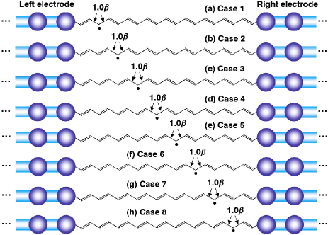
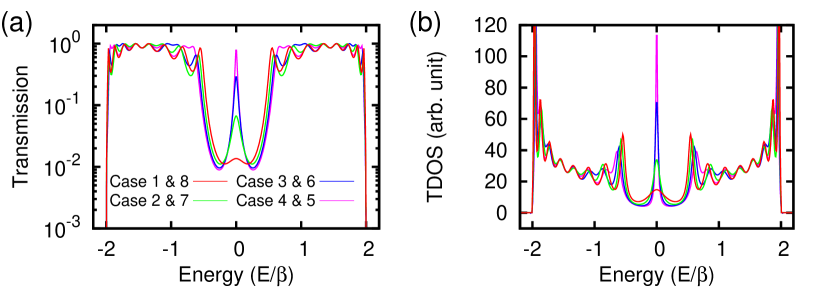
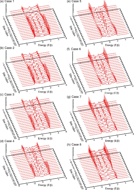
Figure 2 shows modeled poly-acetylene-based (PA-based) molecular wires consisting of 19 sites connected between 1D electrodes and allowing for possible 8 soliton positions along the molecular wires. Transfer integrals associated with double bonds and single bonds are set to and , respectively. The two hopping parameters on either side of the soliton site are set to . All on-site energies are set to . The coupling constants to the electrodes are set as . The 1D electrodes are treated by the Newns-Anderson modelAnderson1 ; Anderson2 with and . Fermi energy is set to .
Fig. 3 shows calculated transmission spectra and TDOS of the 1D molecular systems with different soliton positions. Interestingly, depending on the position of the soliton, the transmission at the Fermi energy () changes drastically (See animation in Supplemental Information). When the soliton lies near an electrode, the resonances in the transmission spectra and TDOS at broaden with lower peaks. In this case, in spite of having an odd number of sites, the features of the TDOS and transmission resemble those for the PA-based molecular junctions which have an even number of sites (See Fig. S4(a) or (c) in Supplemental Information). On the other hand, when a soliton lies in the middle of the molecular wire, the resonances in the transmission spectra and TDOS sharpen and get narrower. The value of the transmission at approaches its theoretical maximum of 1.0.
In order to elucidate the relationship between the positions of a soliton and sharpness of resonant peaks, the distribution of LDOS along the molecular framework was calculated. Figure 4 shows the LDOS surface plot as a function of energy and site index. The LDOS surface plot has peaks near the Fermi energy () where the soliton is located. The LDOS peaks at broaden and reduce in height when the soliton is located at the terminal of the molecular wire (Fig. 2(a) and (h)), whereas the LDOS peaks at sharpen and narrow when the soliton is located in the middle of molecule (Fig. 2(d) and (e)).
This feature can be explained as follows. When a soliton lies at the terminal of a molecular wire, the localized state on the molecular wire strongly interacts with surface states of the lead broadening the LDOS peaks around . This means an electron occupying the soliton state easily escapes back to the electrode where the electron was injected from, so that the chance of the electron traveling through to the other electrode is reduced resulting in low transmission at . Meanwhile, when a soliton lies at the center of a molecular wire, the localized state of the molecular wires interacts symmetrically and weakly with surface states of the two leads producing sharp LDOS peaks.
This conclusion can also be understood in terms of the generalized symmetry condition.Azbel ; Luis ; DPW89 ; LPD90 The transmission peak close to the resonance is approximately described as , where is the energy of the molecular orbital associated to the soliton. follows a simple relation, , where is the orbital amplitude of the molecule at the left/right interface. Thus, symmetric coupling of the molecule with two electrodes, , which corresponds to the soliton localization at the center of the molecule in case 4 or 5 in Fig. 2, gives optimal transmission probabilities, while asymmetric coupling, as can be seen in case 1 or 8 in Fig. 2, gives lower transmission probabilities.
III.2 Creation of transmission channels by a defect
We have examined how the position of a soliton modifies the conductance of molecular wires and seen that the conductance is greatly reduced when the soliton lies near electrodes. Here, we investigate the influence of the defect and demonstrate the counter-intuitive result that the introduction of a defect satisfying special conditions creates a transmission channel leading to higher conductance than in defect free systems.
In general, realistic molecular junctions will contain defects. The defects may induce disorder in the molecular framework. In the presence of defects both the on-site energies and the hopping integrals are modified. Therefore, the transport properties of the molecular junctions will also be changed. Thus we need to consider the effect of defects on quantum transport. We will now examine the dependence of the transmission and DOS on the position of the defect. Here we only consider fluctuations in the hopping integrals and introduce a defect as a reduced transfer integral in a molecular system with an even number of sites. For simplicity we consider a single defect in the molecular system.

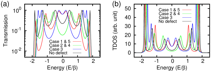
Figure 5 shows the schematic description of 1D molecular wire consisting of 6 sites, with a single defect, coupled to two electrodes. Transfer integrals for nearest neighbors and coupling strength at the left and right interfaces are set to and , respectively. The defect is introduced as a reduction of the transfer integral between the two sites on either side of the defect to a value of . We considered 5 cases of different positions of a single defect on a molecular wire and investigated position-dependence of the transmission and DOS of the molecular wire.
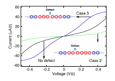
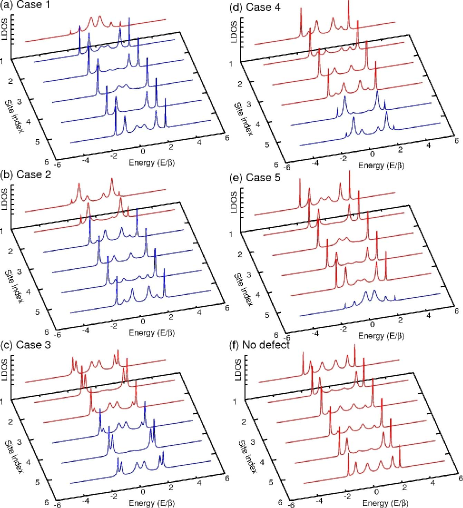
Figure 6 shows the transmission spectra and TDOS of the molecular wire shown in Fig. 5. Depending on the position of the defect, the transport properties change dramatically particularly around . Fig. 7 shows I-V curves of the molecular wire calculated in the linear response regime. Surprisingly, the transmission at in cases 1, 3, and 5 is higher than for defect free systems (Fig. 6).
In order to further analyze this behaviour, we calculated the LDOS as a function of energy and site index. Figure 8 shows the surface plot of LDOS as a function of electronic energy and site index. The position of the defect is illustrated by changing the colour of the LDOS curve from red to blue on either side. When a defect is introduced such that the molecular wire is divided into two fragments which have an odd number of sites, for example , the LDOS plot of each fragment, as shown in Fig. 8(c), resembles that of a linear chain having 3 sites () without defects, as shown in Fig. 3(a). The LDOS in Fig. 8(c) shows non-negligible split peaks around . Likewise when a defect is introduced such that the molecular wire is divided into fragments containing or sites, the LDOS plot of longer fragment resembles that of a linear chain having 5 sites () without defects as can be seen in Fig. 3(b). The LDOS in Fig. 8(a) and (e) show non-negligible split peaks around . This is why, despite including the single defect, these cases lead to higher transmission probabilities and TDOS around than the defect free systems shown in Fig. 6 and Fig. 7.
On the other hand, when the defect is introduced such that the molecular wire is divided into two fragments both having an even number of sites, for example , the LDOS plot of each fragment resembles that of a linear chain having an even number of sites without defects. The LDOS in Fig. 8(b) and (d) are small around . Thus, these cases lead to low transmission probabilities and TDOS around as shown in Fig. 6.
IV Conclusion
In summary, in order to elucidate the factors controlling charge transport through 1D molecules connected between electrodes we have modeled molecular junctions using the tight-binding method. Then we calculated the the influence of the parameters including molecular lengths, degree of dimerization, odd-even effects, soliton formation, and defects on transport properties of the molecular junctions at equilibrium using the Landauer approach combined with the Green’s function formalism.
The numerical calculations have shown that the transport properties at the Fermi energy () dramatically change depending on the degree of dimerization and on whether the number of the sites is odd or even. It has been shown that dimerization of the molecular wires associated with Peierls distortion reduces the DOS at the Fermi energy, leading to exponential decay of length dependence of conductance of the molecular wires. We also proved that the damping factor is closely related to the degree of dimerization of the molecular wires. Interestingly, the longer chain system without dimerization showed no decay in the conductance at the Fermi energy. In the case of molecular wires with an odd number of sites, the extra non-bonding state appears in the middle of the band gap contributing to high conductance at low bias. Additionally, in the molecular wires with an odd number of sites, the conductance at the Fermi energy was independent of the length of the molecular wires.
Our calculations also demonstrate that the transport properties are highly sensitive to the position of solitons and defects. When a soliton lies near one electrode it strongly interacts with surface states of that electrode giving rise to a low, broad peaks in the zero-bias conductance, while when a soliton lies in the middle of the molecular wire, the interaction of the localized state with the electrodes is weaker leading to high conductance at the Fermi energy with sharp resonant peak. Concerning on the calculation of the influence of defects, we obtained a counter-intuitive result that in some cases defects increase the zero-bias conductance. Our findings are that a defect which divides the molecular wire into two fragments both having an odd number of sites creates a new conduction channel and enhances the zero-bias conductance. Since thermal fluctuation naturally creates this sort of defects that, at least for a while, strongly favors charge transfer, we might infer that this is one of the underlying mechanisms of transport at room temperature. We believe that the presented systematic study could be predictive for a wider material (e.g. semiconductor/organic interfaces). Our results could guide the synthesis of novel molecular wires with enhanced conductors.
Acknowledgments
This work was partially funded by the Volkswagen Foundation and by the WCU (World Class University) program through the Korea Science and Engineering Foundation funded by the Ministry of Education, Science and Technology (Project No. R31-2008-000-10100-0), and the European Social Funds in Saxony and the cluster of excellence ”ECEMP – European Centre for Emerging Materials and Processes Dresden” within the excellence initiative of the Free State of Saxony. We acknowledge the Center for Information Services and High Performance Computing (ZIH) at the Dresden University of Technology for computational resources. The work of Horacio M. Pastawski was possible under the Eramus Mundus Master’s Program at Biotechnologische Zentrum (BIOTEC). We thank Claudia Gomes da Rocha, Cormac Toher, and Luis Foà Torres for useful discussions.
Appendix A Theoretical framework
We model a molecular junction by connecting a 1D molecular wire between two electrodes. For clarity we model the electrodes as 1D wires. We describe this system using a tight-binding Hamiltonian, considering only orbitals. The tight-binding parameters used depend explicitly on the interatomic distances in real space. Thus, we can introduce defects or disorder by directly controlling on-site energies (diagonal elements) and hopping integrals (off-diagonal elements) of the electronic tight-binding Hamiltonian matrices.
Figure 1 shows the molecular junction considered in this work. Our starting point is to divide the entire 1D system into three regions; left electrode, right electrode, and central molecular region. We write the electronic Hamiltonian as
where , , and are respectively the Hamiltonian matrices for the left/right electrodes, for the the central molecular region, and the matrix representing the coupling between the central molecule and the left/right electrodes. In this case, we considered only nearest neighbor interactions, so that the terms are scalar values. The matrix elements of are given by , where and are on-site energies and hopping integral between -th and -th atomic orbitals, respectively. In this study, the electrodes are approximated as semi-infinite 1D chains with a single-orbital per site, thus the Hamiltonians of the semi-infinite electrodes have similar forms with . For simplicity we only consider the interaction between nearest neighbors. The matrix elements of left/right electrodes are given by . Hereafter we normalize all hopping integrals, and , in terms of and set all on-site energies as 0, .
In the orthogonal basis the retarded Green function is given by
where , , and are the identity matrix, the positive infinitesimal, and the self energy in the left/right electrode, respectively. The self-energy term is defined as , where is the surface Green function of left/right 1D electrode. The left/right electrode consists of equally spaced 1D sites and coupling between nearest neighbors is set as . The surface Green function of the electrode consisting of equally spaced 1D sites considering only nearest neighbor interaction can be analytically described by the Newns-Anderson modelAnderson1 ; Anderson2 as whose derivationEmberly is summarized in Appendix B.
The conductance of a molecular junction in a low bias is estimated from Landauer’s formula , where is the conductance quantum and is the electronic transmission probability. is obtained from the Fisher-Lee relationFisher-Lee : , where is the broadening function defined as . The DOS is calculated from following equation:
In this study we only consider coherent transport and ignore internal scattering effects such as inelastic transport or incoherent transportNozaki associated with electron-phonon coupling.Frederiksen ; Ryndyk
Appendix B Analytic solution of surface green function in semi-infinite 1D electrode
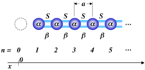
Here we derive the analytic solution of surface green function of a semi-infinite 1D electrode consisting of equally spaced sites. Consider a semi-infinite 1D electrode with lattice constant as shown in Fig. 9. Each site has only one orbital whose position is given by and its on-site energy is . We only consider the interaction between nearest neighbors. The hopping integral and overlap between nearest neighbors are and , respectively. Energy-dependent coupling between nearest neighbors is defined as .
The wave function of semi-infinite electrode can be constructed from forward- and backward-propagating plane wave :
The bra and ket are defined as
Thus, the wave function at site is given by:
This function satisfies the boundary condition of semi-infinite 1D electrode that the wave function on site is zero since .
The operator of Green’s function is defined as
The free propagator of the electrode between sites and is given by
Especially in the case of we get
We only need the matrix element at the terminal site since this is the only site where the molecular system couples, thus putting gives
Hereafter we drop from . Since the number of sites is very large thus the summation can be converted into integral () leading to
Using E-k relation of 1D electrode consisting of equally spaced sites (), we get
When we define , the variable of integral can be changed as
When we define , then we get , , and . Substituting these expressions into , we obtain
where . The term can be changed to . These and must satisfy following relations: and . Note that satisfies these relations. Then is written as
| (1) |
We can solve this complex integral using residue theorem:
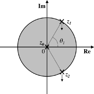
Figure 10 shows the singular points of function on complex variable plane. The residual term for Res vanishes since the imaginary positive infinitesimal term move the singular point at outside of the circle. Therefore, is
where
and
Finally, we get the surface green function of 1D electrode consisting of equally spaced sites as
where, is energy-dependent coupling strength between the electrode and molecule in non-orthogonal description, where is the overlap between the terminal site in the electrode and the molecule.
References
- (1) Cuniberti G, Fagas G and Richter K, Eds. 2005 Introducing Molecular Electronics. (Springer-Verlag Berlin Heidelberg)
- (2) Agraït N, Levy-Yeyati A and van Ruitenbeek J M 2003 Phys. Rep. 377 81
- (3) Hisamoto D, Lee W-C, Kedzierski J, Takeuchi H, Asano K, Kuo C, Anderson E, King T-J, Bokor J and Hu C 2000 IEEE, Trans. Elec. Dev. 47 2320
- (4) Chang P-C, Fan Z, Chien C-J, Stichtenoth D, Ronning C and Lu J G 2006 Appl. Phys. Lett. 89 133113
- (5) Huang Y, Duan X, Cui Y and Lieber C M 2002 Nano Lett. 2 101
- (6) Singh N, Agarwal A, Bera L K, Liow T Y, Yang R, Rustagi S C, Tung C H, Kumar R, Lo G Q, Balasubramanian N and Kwong D-L 2006 IEEE, Elec. Dev. Lett. 27 383
- (7) Ohnishi H, Kondoh Y and Takayanagi K 1998 Nature 395, 780
- (8) Yanson A I, Bollinger G R, vand den Brom H E, Agraït N and van Ruitenbeek J M 1998 Nature 395 783
- (9) Smit R H M, Untiedt C, Rubio-Bollinger G, Segers R C and van Ruitenbeek J M 2003 Phys. Rev. Lett. 91 076805
- (10) Bettini J, Sato F, Coura P Z, Dantas S O, Galvão D S and Ugarte D 2006 Nature Nanotechnol. 1 182
- (11) Nilius N, Wallis T M and Ho W 2003 Phys. Rev. Lett. 90 186102
- (12) Jin C, Lan H, Peng L, Suenaga K and Iijima S 2009 Phys. Rev. Lett. 102 205501
- (13) Chuvlin A, Meyer J C, Algara-Siller G and Kaiser U 2009 New J. Phys. 11 083019
- (14) Landauer R 1981 Phys. Lett. 85A 91
- (15) Büttiker M 1986 Phys. Rev. Lett. 57 1761
- (16) Ellenbogen J C and Love J C 2000 Proceedings of the IEEE 88 386
- (17) Joachim C, Gimzewski J K and Aviram A 2000 Nature 408 541
- (18) Cui Y, Wei Q, Park H and Lieber C M 2001 Science 293 1289
- (19) Patolsky F, Zheng G, Hayden O, Lakadamyali M, Zhuang X and Lieber C M 2004 Proc. Natl. Acad. Sci. USA 101 14017
- (20) De Cola L Ed. Molecular Wires: From Design to Properties. Top. Curr. Chem. 257 (Springer-Verlag Berlin Heidelberg, 2005).
- (21) Calev Y, Cohen H, Cuniberti G, Nitzan A and Porath D 2004 Israel J. Chem. 44 133
- (22) Lang N D 1997 Phys. Rev. Lett. 79 1357
- (23) Forrest S R 2004 Nature 428 911
- (24) Burroughes J H, Bradley D D C, Brown A R, Marks R N, McKay K, Friend R H, Burns P L and Holmes A 1990 Nature 347 539
- (25) Friend R H, Gymer R W, Holmes A B, Burroughes J H, Marks R N, Taliani C, Bradley D D C, Dos Santos D A, Brédas J L, Lögdlund M and Salaneck W R 1999 Nature 397 121
- (26) Kulkarni A P, Tonzola C J, Babel A and Jenekhe S A 2004 Chem. Mater. 16 4556
- (27) Katz H E, Bao Z and Gilat S L 2001 Acc. Chem. Res. 34 359
- (28) Grätzel M 2001 Nature 414 338
- (29) Günes S, Neugebauer H and Sariciftci N S 2007 Chem. Rev. 107 1324
- (30) Blom P W M, Mihailetchi V D, Koster L J A and Markov D E 2007 Adv. Mater. 19 1551
- (31) Chiang C K, Fincher Jr. C R, Park Y W, Heeger A J, Shirakawa H, Louis E-J, Gau S C and MacDiarmid A G 1977 Phys. Rev. Lett. 39 1098
- (32) Chiang C K, Dury M A, Gau S C, Heeger A J, Louis E-J, MacDiarmid A G, Park Y W and Shirakawa H 1978 J. Am. Chem. Soc. 100 1013
- (33) Gregg B A 2009 J. Phys. Chem. C 113 5899
- (34) Su W P, Schrieffer J R and Heeger A J 1979 Phys. Rev. Lett. 42 1698
- (35) Mujica V, Kemp M and Ratner M A 1994 J. Chem. Phys. 101 6849
- (36) Mujica V, Kemp M and Ratner M A 1994 J. Chem. Phys. 101 6856
- (37) Pastawski H M, Weisz J F and Albanesi E A 1995 Phys. Rev. B 52 10665
- (38) Pastawski H M and Medina E 2001 Rev. Mex. Fis. 47s1 1
- (39) Tyler D R 2007 Frontiers in transition Metal-Containing Polymers (Wiley-Interscience, Weinheim, Germany)
- (40) Bera J K and Dunbar K R 2002 Angew. Chem. Int. Ed. 41 4453
- (41) Peierls R E 1955 Quantum Theory of Solids (Clarendon Press; Oxford, U.K.)
- (42) Conwell E M 1988 Semiconductors and Semimetals (Academic Press: Dordrecht, Netherlands)
- (43) Anderson P W 1961 Phys. Rev. 124 41
- (44) Newns D M 1969 Phys. Rev. 178 1123
- (45) Ricco B and Azbel M Y 1984 Phys. Rev. B 29 1970
- (46) Foà Torres L E F, Pastawski H M and Makler S S 2001 Phys. Rev. B 29 193304
- (47) D’Amato J L, Pastawski H M and Weisz J F 1989 Phys. Rev. B 39 3554
- (48) Levstein P R, Pastawski H M and D’Amato J L 1990 J. Phys.: Condens. Matter 2 1781
- (49) Emberly E G and Kirczenow G 1998 Phys. Rev. B 58 10911
- (50) Fisher D S and Lee P A 1981 Phys. Rev. B 23 6851
- (51) Nozaki D, Girard Y and Yoshizawa K 2008 J. Phys. Chem. C 112 17408
- (52) Ryndyk D A and Cuniberti G 2007 Phys. Rev. B 76 155430
- (53) Frederiksen T, Brandbyge M and Jauho A-P 2004 J. Comp. Elec. 3 423